ATCA-based ATLAS FTK input interface system
Abstract
The first stage of the ATLAS Fast TracKer (FTK) is an ATCA-based input interface system, where hits from the entire silicon tracker are clustered and organized into overlapping - trigger towers before being sent to the tracking engines. First, FTK Input Mezzanine cards receive hit data and perform clustering to reduce data volume. Then, the ATCA-based Data Formatter system will organize the trigger tower data, sharing data among boards over full mesh backplanes and optic fibers. The board and system level design concepts and implementation details, as well as the operation experiences from the FTK full-chain testing, will be presented.
keywords:
ATLAS Fast TracKer; FTK; Clustering; Data Formatting; full mesh ATCA; Trigger concepts and systems; Data acquisition concepts1 Introduction
The ATLAS Fast TracKer (FTK) is a Phase-I upgrade program for the ATLAS trigger system [1, 2]. The ATLAS baseline trigger system consists of hardware-based Level-1 trigger and software-based Higher Level Trigger (HLT). The FTK is a hardware-based tracking processor for HLT. It performs global track reconstruction after each Level-1 trigger accept signal, in order to enable the HLT algorithms to have early access to tracking information. FTK will use the entire silicon tracking system of about 100 million channels, consisting of the silicon pixel (Pixel) and micro-strip detectors (semiconductor tracker; SCT), as well as the new Insertable B-Layer (IBL) pixel detector [3]. The availability of the tracking for entire detector, as well as the vertex information at the beginning of HLT will aid in the improvement of HLT algorithms, such as b-tagging and tau-identification.
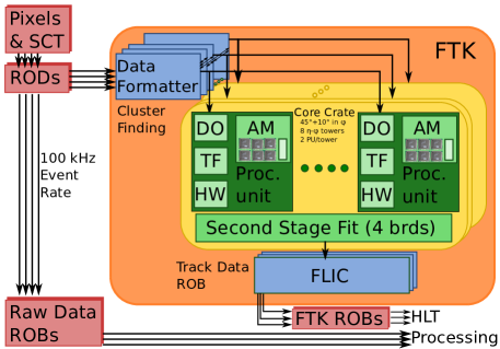
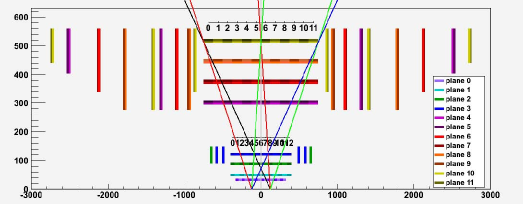
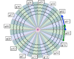
The FTK is a pipeline of dedicated electronics as shown in Figure 1. FTK is highly parallel to deal with the large input data rate, as well as the hit combinatorics due to high occupancy at higher luminosity. The system is segmented into 64 overlapping - trigger towers (Figure 2), with its own pattern recognition and track fitter hardware units. The towers must overlap to avoid inefficiency at tower boundaries due to the finite size of the beam luminous region in the coordinate and the finite curvature of charged particles in the magnetic field. Considering the parallel processing structure, the ATLAS FTK requires its first stage to perform first clustering and then data formatting while data are read. The clustering reduces the data volume and improves the coordinate resolution. Data formatting is then needed to distribute the clusters to appropriate trigger - towers, mapping the silicon detector readout structure to the FTK - structure. The system receives raw hits from Pixel, SCT and IBL ReadOut Drivers (RODs) after the Level-1 trigger decision, and delivers the data to the tracking processor units after clustering and data formatting. This system is denoted as an ATCA-based ATLAS FTK input interface system in this paper.
2 Design concept
The system-level design of the input interface system is dominated by data formatting requirements. We analyzed the required data sharing between the input and output of the system, using real beam data with the actual readout cable mapping. The raw silicon hit data are input to the FTK system over about 400 fibers from silicon RODs (input), and sent to the FTK - towers through about 1,100 fibers (output). The input fibers are assigned to output FTK - towers, so as to minimize the data sharing in the analysis. Figure 3 shows data sharing that is needed among the FTK - towers in the matrix after optimizing the input link assignments. Off diagonal elements represent the data sharing between different towers. The data sharing among trigger towers must be complex due to needs for remapping the silicon detector readout structure into 64 FTK trigger - tower partitioning and overlapping between neighboring towers.
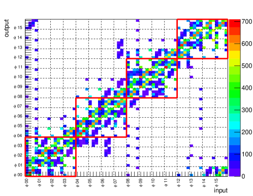
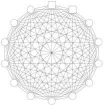
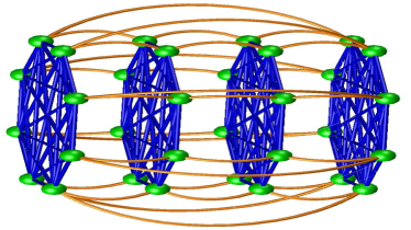
The four red boxes in the matrix, which represent crate boundaries, show that a four-crate system fits the data formatting requirement. Boards within each crate communicate over the backplane. Fiber links need to be used when boards must communicate across crate boundaries. Further, our analysis shows that the data sharing between trigger towers is highly dependent upon upstream cabling and detector geometry. The ideal data formatting hardware platform should be flexible enough to accommodate future expansion and allow for changes in input cabling and module assignments. Based on the requirements, the full mesh Advanced Telecommunication Computing Architecture (ATCA) [4] backplane was found to be a natural fit. The Fabric Interface of the full mesh backplane enables high speed point-to-point communication between every slot (Figure 4 (a)), with no switching or blocking. Each line in this diagram represents a channel, consisting of up to four bidirectional lanes, which runs at a combined maximum speed of up to 40 Gb/s. Assuming that we use 32 boards for the data formatting engines to deal with all 64 FTK - towers, Figure 4 (b) shows a network topology that meets the data formatting requirements in the four full mesh backplanes.
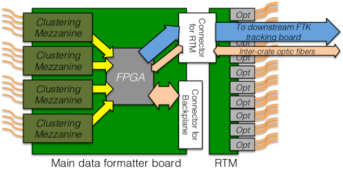
Each board consists of three main components, as shown in the board-level design concept of Figure 5: 1) four mezzanine cards (FTK Input Mezzanines; FTK IMs) to receive the input links and perform the clustering, 2) a data formatting custom ATCA front board (Data Formatter front board; DF), and 3) a rear transition module (RTM) to deal with the fibers for downstream links, as well as the internal links beyond the crate boundary. First the FTK IM receives the input raw silicon hit data. Then clustering is performed by Field Programmable Gate Arrays (FPGAs) equipped on the mezzanine card. The found clusters are then sent to the mother board FPGAs, which are used as the data formatting engines. High speed serializer components in the FPGA are directly connected to the full mesh backplane fabric interface channels, and also to pluggable fiber transceivers located on the RTM, used for interconnection among the DF shelves, and output links to downstream FTK processors.
3 Hardware and firmware implementation
32 DF boards will be used to handle 64 FTK - towers, where four FTK IMs connect to each DF board and 128 FTK IMs will be used in total. We have developed the DF front board, RTM and FTK IM hardware, as well as the firmware for data formatting and clustering. This section will describe details of the implementation for the DF in Section 3.1, for the FTK IM in Section 3.2, and for the user control interface in Section 3.3.
3.1 Data Formatter
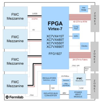
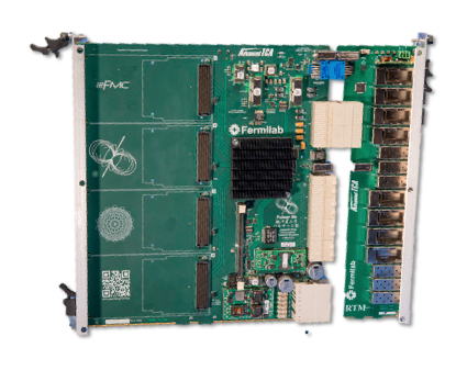
The block diagram of the DF board is shown in Figure 6. The DF front board is designed around a Xilinx Virtex-7 FPGA (XC7V690T-2) [5]. Each board supports up to four FPGA Mezzanine Card (FMC) [6] modules for the FTK IMs. The FPGA has 80 high-speed built-in serial transceivers (GTH) [7] which support data rates up to 10 Gb/s. Of these 80 GTH transceivers, 28 connect to the fabric interface, 40 connect to the RTM, and the other 12 connect to the FMC connectors. The performance of GTH serial lines has been extensively tested and characterized with a bit error rate test (measured upper limit of bit error rate is less than ), as well as a receiver margin analysis (or a statistical eye scan). The data traffic at 10 Gb/s has been proven to run stably on the DF board, while 6 Gb/s is required for the FTK data formatting needs.
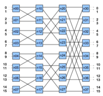
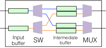
The major challenge of the firmware implementation for the data formatting is to perform high bandwidth routing with low latency and flexible real time data sharing, so that each board handles input lanes from the FTK IM (up to 16 lanes), output lanes to downstream FTK tracking boards (38 lanes), and internal communication lines connecting (18 lanes) to the full mesh ATCA backplane and the inter-crate optic fibers. A switch architecture with a banyan network is selected as the solution. Figure 7 (a) shows an example of the architecture with 16 input and 16 output lanes (16-in-16-out). Each switch element of the matrix structure contains first-in-first-out memories (FIFOs) for internal buffering besides switching and multiplexing functions (Figure 7 (b)) so that data blocking can be minimized with manageable resource usage. The actual resource usage is approximately 70%, where the firmware is equipped with three of 32-in-32-out switches.
The DF has the nickname Pulsar II. Although it was originally motivated by the FTK data formatting needs, it has proven to be generally useful in scalable system where highly flexible non-blocking, high bandwidth board-to-board communication is required. An example is the Level-1 silicon-based tracking trigger R&D for CMS, where the full mesh backplane is used effectively for sophisticated time-multiplexing data transfer schemes [8, 9, 10].
3.2 FTK Input Mezzanine for clustering
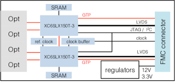
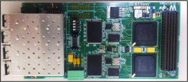
The FTK IM is a custom FMC module and a mezzanine card compatible with the DF mother board. The block diagram of the FTK IM is shown in Figure 8. It is equipped with two Xilinx Spartan-6 LX150T-3 FPGAs [11], four optical transceiver using the SFP to receive the input data from silicon RODs, and an FMC connector to the DF board. Each input SFP optical module connects to a GTP transceiver channel in the Spartan-6 FPGA running up to 3.2 Gb/s. S-LINK protocol [12] is used for the input links from RODs, running at 2.0 Gb/s. Each FPGA on the FTK IM connects to two optical modules. The FPGAs are used as the main engines for clustering, the logic of which is implemented with two decoupled stages: cluster finder and centroid calculators [13]. Finally, the FTK IM sends the found clusters to the DF board by using 16 Double Data Rate (DDR) LVDS parallel buses running at 200 MHz over FMC connectors, allowing a data throughput of 32-bit words at 50 MHz with eight LVDS pairs per lane. The interface is implemented according to the FMC standard, and provides a JTAG chain for FPGA programming, I2C for control path, high-speed transceiver channels, power distribution, and clock distribution in addition to the LVDS parallel data bus.

It is a major challenge to maintain manageable processing time of 2D cluster finding for the pixel sensors at the highest target luminosity of the FTK operation. In fact, the 2D structure of FPGA logic cells is suitable for mapping the 2D structure of sensors, which allows the finder to avoid too many hit loops in the following way. The finder logic starts with the first received hit (blue cell in Figure 9), the order of which has been sorted prior to the cluster finding. It defines the cluster window ( pixel size) with respect to the first hit position so that the logic does not need to map entire pixel modules. This is called the sliding window technique, and allows for an efficient resource usage. Then the logic loads all hits within the window. Once all hit data are loaded, the logic selects all the hits neighboring the first hits within one clock cycle. This is the key step of the algorithm that avoids too many hit loops to maintain manageable processing time. The hit selection is continued until there is no neighboring hit. Eventually the selected hits are sent to the centroid calculator as a cluster. This way the full implementation fits in approximately 60% of the available Spartan-6 resources.
3.3 User control interface
Besides the main data formatting and clustering functions, user control interface has been implemented. ATCA backplanes require two dedicated slots for hub switching boards (Hub Slots) with two separate dual-star networks, called Base Interface for slow controls and Fabric Interface for high-speed transfers (up to 40G Ethernet). A DF FPGA connects to one of the two Hub Slots through Fabric interface with four lanes up to 40 Gb/s for the Ethernet communication. For the board control, we have adapted the CMS IPbus framework [14] to the system. UDP packets are transferred between external computers (IPbus clients) and the DF boards (IPbus devices) through a hub switching board. Further I2C bus signals for FTK IM may be controlled over the IPbus interface so that the control path from external computers is available for both DF main boards and FTK IMs.
4 System-level demonstration
We have established an ATCA test-stand at CERN in order to demonstrate the system-level operation in terms of both the control path and data-flow. Prototype DF boards and FTK IMs were integrated after the single board testing. The control path with IPbus and I2C has been established in the CERN General Purpose Network environment. One computer in the CERN network is setup as the IPbus client on which an end-user application runs MicroHAL software. The IPbus transactions are routed via the Control Hub node, which is packet-handling software that allows separation of hardware and control network, for safe transport of IPbus commands. For data-flow demonstration, first we tested communication functionality between neighboring boards with required speed: S-LINK (2.0 Gb/s) between RODs and FTK IM, LVDS parallel bus between FTK IM and DF (200 MHz DDR), and S-LINK (6.0 Gb/s) between DF and downstream FTK tracking boards. Then data-flow demonstration through the system followed the interface functionality tests. Either external optical transmitters which emulate RODs or test input patterns stored in FTK IM internal RAMs are used. The input event rate and data pattern can be adjusted, and the goal of the demonstration is to process simulation data with the highest target luminosity at 100 kHz input Level-1 trigger rate. The clustering algorithm and the data formatting functionality are being tested in the test-stand. As of the end of September, 2014, we’ve demonstrated them with the simplest hardware setup: one input at the maximum input speed of 100 kHz. Scaling up the system is the next major milestone for the demonstration.
5 Conclusion
A clustering and data formatting solution for the ATLAS FTK has been developed, based on full mesh ATCA. We have developed a custom ATCA board for data formatting engine (DF) and a custom FMC module for clustering (FTK IM). Prototype boards and the firmware are being extensively tested to verify the design and are being used for the system-level demonstration at CERN. The initial control path test and data-flow demonstration with the minimum setup has succeeded. The system-level demonstration with full FTK system functionality will be the next major milestone, for the FTK system commissioning planned in later 2015 during LHC Run2.
References
- [1] ATLAS Collaboration, The ATLAS Experiment at the CERN Large Hadron Collider, JINST 3 S08003, 2008
- [2] ATLAS collaboration, Fast TracKer (FTK) Technical Design Report, CERN-LHCC-2013-007 ATLAS-TDR-021
- [3] The ATLAS Collaboration, ATLAS Insertable B-Layer Technical Design Report, CERN-LHCC-2010-0013
- [4] PICMG 3.0 AdvancedTCA Base Specification (Shortform), http://www.picmg.org/v2internal/shortformspecs.htm
- [5] Xilinx Inc, 7 Series FPGAs Overview, http://www.xilinx.com/support/documentation/data_sheets/ds180_7Series_Overview.pdf
- [6] FPGA Mezzanine Card Specification (VITA57.1), http://www.vita.com/fmc.html
- [7] Xilinx Inc, 7 Series FPGAs GTX/GTH Transceivers User Guide, http://www.xilinx.com/support/documentation/user_guides/ug476_7Series_Transceivers.pdf
- [8] PulsarII project web page (ATCA at Fermilab), http://www-ppd.fnal.gov/ATCA/
- [9] J. Olsen et al, A full mesh ATCA-based general purpose data processing board, JINST 9 C01041, Topical Workshop on Electronics for Particle Physics 2013 (TWEPP-13), 2014
- [10] Y. Okumura et al, Prototype performance studies of a Full Mesh ATCA-based General Purpose Data Processing Board, FERMILAB-CONF-13-527-CMS-PPD, arXiv:1403.4331, Nuclear Science Symposium and Medical Imaging Conference (NSS/MIC) 2013 IEEE, 2013
- [11] Xilinx Inc, Spartan-6 Family Overview, http://www.xilinx.com/support/documentation/data_sheets/ds160.pdf
- [12] CERN S-LINK homepage, http://hsi.web.cern.ch/HSI/s-link/
- [13] C.-L. Sotiropoulou et al, A multi-core FPGA-based clustering algorithm for real-time image processing, Nuclear Science Symposium and Medical Imaging Conference (NSS/MIC), 2013 IEEE, 2013
- [14] CACTUS project: SW and F/W repository and tracking system for the upgrades of the CMS level-1 trigger webpage, https://svnweb.cern.ch/trac/cactus