Quasi-classical Theory of Tunneling Spectroscopy in Superconducting Topological Insulator
Abstract
We develop a theory of tunneling spectroscopy in superconducting topological insulator (STI), i.e. superconducting state of a carrier-doped topological insulator. Based on the quasi-classical approximation, we obtain an analytical expression of the energy dispersion of surface Andreev bound states (ABSs) and a compact formula for tunneling conductance of normal metal/STI junctions. The obtained compact formula of tunneling conductance makes the analysis of experimental data easy. As an application of our theory, we study tunneling conductance in CuxBi2Se3. We reveal that our theory reproduces the previous results by Yamakage et al [Phys. Rev. B 85, 180509(R) (2012)]. We further study magneto-tunneling spectroscopy in the presence of external magnetic fields, where the energy of quasiparticles is shifted by the Doppler effect. By rotating magnetic fields in the basal plane, we can distinguish between two different topological superconducting states with and without point nodes, in their magneto-tunneling spectra.
1 Introduction
Topological superconductors have gathered considerable interests in condensed matter physics.[1, 2, 3, 4, 5]. They are characterized by the existence of surface states stemming from a non-trivial topological structure of the bulk wave functions.[1] These surface states are a special kind of Andreev bound states (ABSs), which are known as Majorana fermions.[3, 4] It is believed that the non-Abelian statistics of Majorana zero modes open a new possible way to fault tolerant quantum computation.[6] There are many works on this topic and several proposals for systems where topological superconductivity is expected to be realized. [7, 8, 9, 10, 11, 12, 13, 14, 15, 16, 17, 18, 19, 20, 21, 22, 23, 24]
One of the most promising candidates of topological superconductor is Cu doped Bi2Se3 [25, 26, 27]. Since its host undoped material is a topological insulator, this material is dubbed as superconducting topological insulator (STI). Theoretically, Fu and Berg classified the possible pair potentials which are consistent with the crystal structures.[28] They considered four different irreducible representations of gap function, based on the two orbital model governing the low energy excitations.
According to the Fermi surface criterion for topological superconductivity [29, 28, 30], it has been revealed theoretically that ABSs are generated as Majorana fermion for odd-parity pairings in the , and irreducible representations. Among these pairings, and pairings have gapless ABSs in the (111) surface. [31, 32, 33] While the pair potential in does not have nodes on the Fermi surface, the pair potential in has point nodes on the Fermi surface. For both pairings, the resulting ABSs have a structural transition in the energy dispersion.[33] In the tunneling conductance between normal metal / insulator / CuxBi2Se3 junctions, the gapped pairing shows a zero bias conductance peak (ZBCP) for high and intermediate transparent junctions and a zero bias conductance dip (ZBCD) for low transparent junctions. [33] On the other hand, always shows a ZBCP. [33]
In experiments, a pronounced ZBCP has been reported in point contact measurements of CuxBi2Se3. [26] While there are other reports which have observed similar ZBCPs [34, 35, 36, 37], there also exist conflicting results [38, 39], where a simple U-shaped tunneling conductance without ZBCP has been reported by the scanning tunneling microscope (STM). For the latter experiments, however, a recent theoretical study of proximity effects on STI has suggested that the simple U-shaped spectrum is not explained by an -wave superconductivity of CuxBi2Se3[40]. Although there are several studies on electronic properties of superconducting states in CuxBi2Se3, the pairing symmetry of this material has not been clarified yet. [41, 42, 43, 44, 45, 46, 47, 48]
Since the experiments of tunneling spectroscopy have not been fully settled at present, it is desired to derive a compact and simple formula of tunneling spectroscopy of STI. Indeed, the previous theory of tunneling spectroscopy needs a complicated numerical calculation, and thus it is not sufficiently convenient to fit experimental data. It is not so easy to grasp an intuitive picture of STI as well. [33] To improve them, we use here the quasi-classical theory of STI. Although there are two orbitals in the microscopic Hamiltonian, the resulting Fermi surface of STI is rather simple. Hence, it has been proposed to construct a quasi-classical theory of STI by extracting low energy degrees of freedom on the Fermi surface. [43, 44, 45]
If we can derive a more convenient theory of tunneling conductance by using the quasi-classical approximation, our understanding on the tunneling spectroscopy of STI can be much more clear since the intuitive picture on the relation between ABS[49, 50, 51] and tunneling conductance is expected to be obtained.[52, 53] We also expect that the theory is useful like the quasiclassical theory of charge transport in -wave superconductor junctions [54, 55, 56, 57]
In this paper, starting from a microscopic Hamiltonian of topological insulators, we develop the quasiclassical theory of tunneling spectroscopy for STI. We derive analytical formulas of ABSs and tunneling conductance for normal metal / STI junctions. Using the obtained formula of ABSs, the transition in spectrum of ABS, which was reported in Ref.\citenyamakage12, is reproduced. We also calculate the magneto-tunneling conductance in order to extract an information on momentum dependence of pair potentials from tunneling spectroscopy.[58, 59, 60] It is found that we can distinguish between and , although a similar ZBCP appears for both pairings. By rotating magnetic fields on the basal plane parallel to the interface, exhibits a two-fold symmetry in the tunneling conductance due to the existence of point nodes on the Fermi surface.
2 Model and Formulation
2.1 Model Hamiltonian for STI
To study carrier-doped topological insulators, we start from the two-orbital model proposed to describe Bi2Se3.[61, 62] The normal-state Hamiltonian is given by
| (2) | ||||
| (3) |
where . and denote the Pauli matrices in the spin and orbital spaces, respectively. In the superconducting state, the BdG Hamiltonian is given by
| (4) |
where labels the type of the pair potential. In a weak-interaction, where Cooper pairs are formed inside a unit cell, does not have -dependence. In this case, there are six types of pair potentials: , , , , and . and belong to the irreducible representation, and , and belong to the , and irreducible representations, respectively. We choose for in this paper. The results for is obtained by four-fold rotation around -axis, .
Before making a quasiclassical wave function in superconducting state, we first diagonalize the normal state Hamiltonian.
| (5) |
with . labels spin helicity, and and represent the band index. Here, we consider electron-doped Bi2Se3-type topological insulator where only the conduction band has a Fermi surface. In addition, the magnitude of the superconducting energy gap is far smaller than the bulk band gap. Actually, in CuxBi2Se3, the critical temperature ([25]) is much smaller than the band gap ([63]). In this case, the coherence length is much longer than the inverse of the Fermi wavenumber , and the quasiclassical approximation is valid.[64] Then, the intraband pairing in valence band and interband pairing between conduction and valence bands can be neglected. Then, the Bogoliubov de-Gennes Hamiltonian is reduced to one by extracting only the components of conduction band.
| (6) |
Here is the dispersion of the conduction band in the normal state. and are matrices which describe unit matrix and intraband pairing in conduction band, respectively. The intraband pair potentials for conduction band are written as
| (7) | ||||
| (8) | ||||
| (9) | ||||
| (10) | ||||
| (11) |
where
| (12) | ||||
| (13) | ||||
| (14) | ||||
| (15) | ||||
| (16) | ||||
| (17) | ||||
| (18) |
2.2 Analytical Formula of the Andreev Bound States
Solving the effective BdG equation
| (19) |
the wave function for each pair potential is derived as
| (20) | ||||
| (21) | ||||
| (22) | ||||
| (23) | ||||
| (24) |
where is the Fermi momentum defined by . Here the matrix
| (25) | |||
| (26) |
is attached to restore the transformation of the spin basis.
| (30) | |||||
| (34) | |||||
| (41) | |||||
| (45) | |||||
| (52) | |||||
| (59) |
We calculate the energy spectrum of the ABS from these wave functions for semi-infinite CuxBi2Se3 with by imposing the boundary condition . It is clarified that there is no ABSs in and . On the other hand, there exists the ABS in and whose energy spectra are expressed as
| (60) | ||||
| (61) |
with . Equations (60) and (61) are one of the main results of the present paper. In the later section, we explain that the unconventional caldera-type or Ridge-type dispersion of the ABS are produced by .[43]
2.3 Analytical Formula of the Conductance
Next, we calculate tunneling conductance between CuxBi2Se3 () and normal metal (). For normal metal, we consider a single band model with parabolic dispersion . In the normal metal, the wave function is written as
| (62) | |||||
| (63) | |||||
for the injection of the spin up and spin down electron. The four transmission and reflection coefficients are determined by the boundary condition. By considering the delta function barrier potential , the boundary condition is summarized in the form
| (64) | ||||
| (65) | ||||
| (66) | ||||
| (67) |
where and are the Fermi velocities in the -direction inside the normal metal and STI, respectively. They are given by
| (68) | ||||
| (69) |
where is defined by the equation . The other parameters are defined as
| (70) |
| (80) |
| (81) | |||||
| (82) | |||||
| (83) | |||||
| (84) | |||||
| (85) |
By eliminating and in the boundary condition, then
| (86) | |||||
| (87) |
where and . By using these equations, we can aquire the expression of the transmissivity as
| (88) | |||||
Here is the transmissivity when is in the normal state. If we consider the injection of the spin up electron, , the transmissivity is expressed as
| (89) | |||||
On the other hand, if we consider the injection of the spin down electron, , the transmissivity is expressed as
| (90) | |||||
As a result, the transmissivity is expressed as
| (91) | |||||
Equation. (91) is also the main result of the present paper. This conductance formula is a natural extension of that for single band unconventional superconductors.[52, 53] To derive this expression, we used and . This formula of the transmissivity can be simplified as
| (92) | |||
| (93) | |||
| (94) | |||
| (95) | |||
| (96) |
for , , and , respectively. It is remarkable that these equations are essentially the same as the standard formula of transmissivity [52]. Using this transmissivity, the normalized tunneling conductance can be calculated by integrating the angle of the injection of the electron
| (97) |
In the following, we also consider Doppler effect in the presence of magnetic fields parallel to the -plane. If we denote the angle between the magnetic field and the -axis, the magnetic field in the superconductor is given by
| (98) |
for with penetration length . The vector potential is given by
| (99) |
In order to calculate the tunneling conductance, it is sufficient to know the value only near the interface with . Then, the vector potential can be approximated as
| (100) |
The energy of the quasi-particle is shifted as by the Doppler effect. Here, is the magnitude of the in-plane group velocity of quasi-particle and is measured from the -axis.
3 Calculated Results
In this section, we show the calculated results of the ABSs, conductance and magneto-tunneling conductance. For the material parameters , , , , , , we adopt the values for Bi2Se3. [62] Since these parameters proposed in Ref. \citenS-C_Zhang10 give a cylindrical Fermi surface in the tight-binding model, different parameters are proposed in Ref. \citensasaki11 and \citenHashimoto2013. However, the obtained Fermi surface in the present continuum model is the ellipsoidal one in both cases since the Brillouin zone does not exist. Though the Fermi momentum and the Fermi velocity along the -direction are different between these two kinds of parameters, we have confirmed that this difference does not influence the results qualitatively.
3.1 Andreev Bound State
We first outline important features of ABSs we discuss in this paper. Figure 1 illustrates schematic shapes of the dispersion of the ABS in for various values of and .
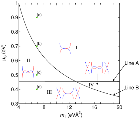
In the region III and IV below line A, it is known that the surface Dirac cone stemming from topological insulator (dotted lines in Fig. 1) and the ABS (solid lines in Fig. 1) are well separated, and the surface Dirac cone exists outside the Fermi momentum . [31, 33] This surface Dirac cone can not be described in the quasiclassical approximation. On the other hand, in the region I and II, the ABS merges with the surface Dirac cone. The group velocity of ABS at becomes zero on line B. In the region I, the shape of the dispersion of the ABS is essentially the same as the standard Majorana cone realized in Balian-Werthamer (BW) phase of superfluid 3He. In the region II, the group velocity of ABS at is negative and the shape of the dispersion becomes caldera-type for . [33] In this region, the dispersion of the ABS is twisted and it crosses zero energy at finite and as well as at , since can be zero in Eq. (60). On the other hand, in the region III, the ABS looks like a conventional Majorana cone again, because the solution of moves outside the Fermi energy. It is noted that the shape of the ABS in the region III is the same as that in the region I, however, the sign of the group velocity at in these two regions are opposite. In this case, the surface Dirac state can not be described in the quasi-classical approximation, but this hardly affects the conductance because the group velocity of this surface Dirac cone is much larger than that of the ABS.
In the case of , as seen from Eqs. (60) and (61), the dispersion of the ABS along -axis is identical with . On the other hand, the energy dispersion of the ABS along -axis is zero-energy flat band. Thus, a ridge-type (valley-type) ABS appears in the region II (region I).

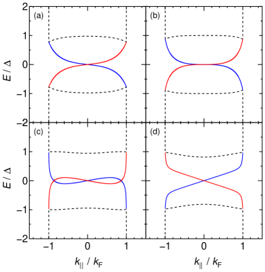

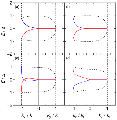
Now let us see more details of ABSs. For , the bulk energy gap is isotropic and there is no ABS. It is essentially the same with that of conventional BCS -wave pairing. For the other type of the pair potential, we show the energy gap of the bulk energy dispersion and ABSs in Figs. 2-5. Since the energy spectra have rotational symmetry in the - plane, we plot bulk energy gap and ABS as a function of except for case. For case, since the spectra does not have this rotational symmetry, we plot and ABS as a function of with in the left side and with in the right side. In each figure, the value of the chemical potential is chosen to be 0.9, 0.7, 0.5 and 0.4 eV (which are shown by dots in Fig.1) for (a),(b),(c) and (d), respectively.
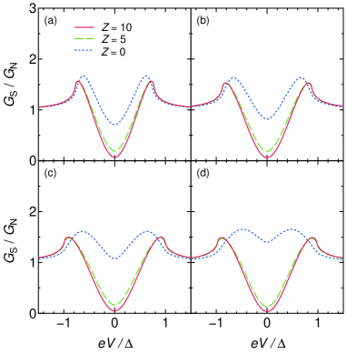
In the case of , though its irreducible representation is the same as , the bulk energy gap has an anisotropy as seen from Eq. (12). Since can be zero in the regions II and IV, line nodes appear in these regions. Thus, the energy gap closes for as shown in Fig. 2(c). In other regions, is fully gapped as shown in Figs. 2(a), (b) and (d). No ABS appears for this gap function as in the case of .
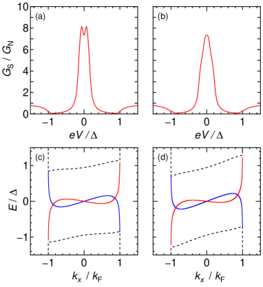
In the case of , the bulk energy dispersion has a fully gapped structures. ABSs are generated on the surface at . In Fig. 3, we plot the dispersion of the ABS by solid lines. As explained in Fig. 1, the line shapes of the dispersion of the ABS changes with the chemical potential. For and 0.7 eV (Figs. 3(a) and (b)), the resulting ABS is the standard Majorana cone as shown in the region I. The group velocity at for is closer to zero than that for , since the values of and is close to those on the line B in Fig. 1. Fig. 3(c) demonstrates a caldera-type dispersion in the region II. At eV, as shown in Fig. 3(d), the line shape of the dispersion of the ABS is similar to the standard Majorana cone like Fig. 3(a) and (b) while the sign of the group velocities of the ABS is opposite.
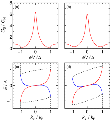
In the case of , the bulk energy gap closes at as seen from Figs. 4(a)-(d). This comes from point nodes at north and south poles on the Fermi surface In this pair potential, the parity of the spatial inversion is odd. On the other hand, the parity of the mirror reflection at is even. There is no ABS at the surface .
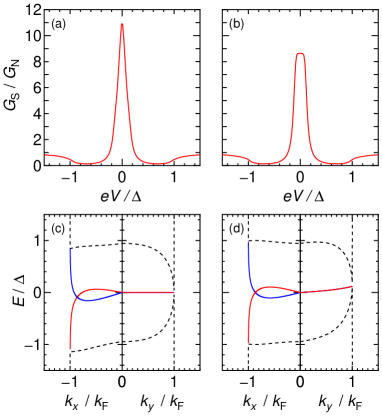
The pair potential belongs to the two-dimensional irreducible representation , and . In the present paper, we choose . As seen from Figs. 5(a)-(d), the bulk energy gap closes along -axis where point nodes exist. In this direction, the dispersion of the ABS is completely flat with zero energy. In a manner similar to , the group velocity of the ABS along -axis decreases with . Then, a ridge-type ABS appears at as shown in Fig. 5(c). In the other cases, a valley-type ABS is generated.
3.2 Conductance
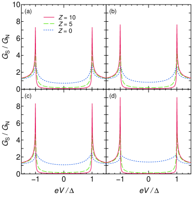
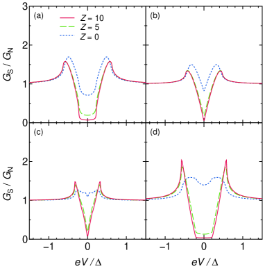
In this subsection, we show the bias voltage dependence of tunneling conductance for all possible pairings, , , , and in Figs. 6, 7, 8, 9 and 10, respectively. For the magnitude of the barrier potential , we choose , 5, and 10 for high, intermediate and low transmissivity, respectively. and are chosen as eV and eV Å2. For , the obtained conductance rarely depends on qualitatively as shown in Fig. 6. For the junction with high transmissivity, a nearly flat nonzero conductance appears around zero voltage. On the other hand, in the case of low transimissivity, the conductance have -shaped structures. These features are standard in conventional spin-singlet -wave superconductors obtained by BTK theory. [65]
In the case of , the resulting conductance has a ZBCD independent of the chemical potential for . For , the conductance has a -shaped structure for (a) eV and (d) eV. On the other hand for (b) eV and (c) eV, we obtain -shaped tunneling conductance due to the highly anisotropic energy gap.
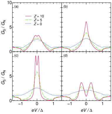
For , the tunneling conductance shows a simple broad peak around zero voltage for as shown in Fig. 8. For , the dispersion of the ABS seriously influences the line shape of the tunneling conductance since the tunneling current flows through the ABSs in the case of low transmissivity. The conductance shows a ZBCD except for the case of eV in Fig. 8(b). A ZBCP appears for eV. This difference originates from the difference in the dispersion of the ABS: The dispersion of the ABS shows the standard Majorana cone like a surface state of BW-phase of superfluid 3He. It has been known that, in the BW-phase, the tunneling conductance has a ZBCD like a curve for in Fig. 8(a).[66, 33] In the parameter regime near line B in Fig. 1, however, the group velocity of the ABS around zero energy is almost zero. Therefore, the surface density of states near the zero energy is enhanced and the resulting tunneling conductance has a ZBCP. On the other hand, if the magnitude of the group velocity is increasing, then the surface density of states near zero energy is reduced. Then, the surface density of states has a -shaped structure and the resulting tunneling conductance can show a ZBCD (see Figs. 8(a), 8(c) and 8(d)).
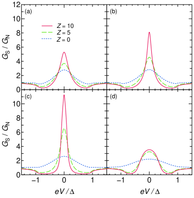
In the case of , the obtained conductance always have ZBCD as shown in Fig. 9. Since there is no ABS in the present junction, conductance for is proportional to around zero voltage reflecting the presence of the point nodes on the Fermi surface.
The conductance in the case of shows a ZBCP peak as shown in Fig. 10. The existence of the flat zero-energy ABS in the direction of induces a ZBCP regardless of the magnitude of the chemical potential.
The calculated results by our analytical formula of conductance well reproduce the preexisting numerical results. [33] This means that the quasi-classical approximation works well in this system. The reason for this is that the present system has a single Fermi surface, where simplified calculation is available.
3.3 Magneto-tunneling conductance
In this subsection, we study magneto-tunneling spectroscopy as an application of this new formula of conductance. Since both and can have ZBCP, it is difficult to distinguish between these two pair potentials by simple tunneling spectroscopy. To resolve this problem, magneto-tunneling conductance is useful to know the detailed structure of the energy gap and the ABS.

We show the ABS and the tunneling conductance for with in the presence of in-plane magnetic fields in Fig. 11. Since the energy dispersion of the quasi-particle is given by , the magnitude of the Doppler shift is prominent when the azimuthal angle of the momentum coincides with the direction of the magnetic field . Thus, the energy dispersion of the ABS is tilted in the direction of the applied magnetic field. Then, the dispersion of the ABS shown in Fig. 3(c) becomes those in Figs. 11(c) and (d) for and , respectively. Because the magnitude of the Doppler shift is proportional to that of the applied field, the value of the group velocity of the one of the edge modes approaches to zero in higher fields, and thus surface density of states near zero energy increases. As a result, the ZBCD structure in the conductance is smeared as shown in Figs. 11(a), and the conductance has a zero bias peak in higher field as shown in Figs. 11(b). These features have never been seen in Doppler effect in high- Cuprate, where the ABS has a flat dispersion [67, 68, 69].
Next, we show the case of eV in Fig. 12. In this case, conductance has a zero bias peak in the absence of the magnetic field as shown in Fig. 8(c) since the group velocity of the ABS is close to zero. In the presence of the magnetic field, group velocities of the two edge channels deviate from zero as shown in 12(c) and (d). Therefore, the height of the ZBCP decreases with magnetic field.
Next, we show the magneto-tunneling conductance for . This pair potential has an in-plane anisotropy. Figure 13 shows the conductance and the ABS with magnetic field in the -direction ((a), (c)) and the -direction ((b), (d)). The resulting conductance depends on the direction of the magnetic field. The height of the ZBCP under magnetic fields in the y-direction (nodal direction) is smaller than that under magnetic fields in the -direction. This is because the flat ABS in the nodal direction is tilted as shown in Fig. 13(d). To see the in-plane anisotropy of the magneto-tunneling conductance, we calculate the magnetic-field angle dependence of the conductance at in Fig. 14. It shows minima when the magnetic field is parallel to the nodal direction.[70] The angular dependence of the conductance appears only for , since other pair potentials have an in-plane rotational symmetry. Thus, we can distinguish between and .
4 Summary
In this paper, we have examined the dispersion of surface ABSs of STI and the tunneling conductance in normal metal/STI junctions by deriving analytical formula based on the quasiclassical approximation. Our obtained results are consistent with the previous numerical calculation by Yamakage [33] which does not use quasiclassical approximation. By using the obtained analytical formula of tunneling conductance, one can easily calculate the tunneling conductance without any special techniques of numerical calculation. In addition, we have calculated the tunneling conductance under external magnetic fields in the -plane by taking account of the Doppler shift. As a result, we have shown that the pair potential and can be distinguished by measuring the field-angle dependence of the zero-bias conductance. In this paper, we have studied ballistic normal metal / STI junctions. The extension of our conductance formula to the diffusive normal metal / STI junction by circuit theory [71]is interesting since we can expect anomalous proximity effect [57] by odd-frequency pairing [72].
Acknowledgements
This work was supported in part by Grants-in-Aid for Scientific Research from the Ministry of Education, Culture, Sports, Science and Technology of Japan ”Topological Quantum Phenomena” (Grant No. 22103005 and No. 25287085) and the Strategic International Cooperative Program (Joint Research Type) from the Japan Science and Technology Agency.
References
- [1] A. P. Schnyder, S. Ryu, A. Furusaki, and A. W. W. Ludwig: Phys. Rev. B 78 (2008) 195125.
- [2] F. Wilczek: Nature Phys. 5 (2009) 614.
- [3] X.-L. Qi and S.-C. Zhang: Rev. Mod. Phys. 83 1057.
- [4] Y. Tanaka, M. Sato, and N. Nagaosa: J. Phys. Soc. Jpn. 81 (2012) 011013.
- [5] J. Alicea: Rep. Prog. Phys. 75 (2012) 076501.
- [6] C. Nayak, S. H. Simon, A. Stern, M. Freedman, and S. Das Sarma: Rev. Mod. Phys. 80 (2008) 1083.
- [7] A. Kitaev: Ann. Phys. 321 (2006) 2.
- [8] L. Fu and C. L. Kane: Phys. Rev. Lett. 100 (2008) 096407.
- [9] Y. Tanaka, T. Yokoyama, A. V. Balatsky, and N. Nagaosa: Phys. Rev. B 79 (2009) 060505.
- [10] M. Sato, Y. Takahashi, and S. Fujimoto: Phys. Rev. Lett. 103 (2009) 020401.
- [11] M. Sato, Y. Takahashi, and S. Fujimoto: Phys. Rev. B 82 (2010) 134521.
- [12] L. Fu and C. L. Kane: Phys. Rev. Lett. 102 (2009) 216403.
- [13] A. R. Akhmerov, J. Nilsson, and C. W. J. Beenakker: Phys. Rev. Lett. 102 (2009) 216404.
- [14] K. T. Law, P. A. Lee, and T. K. Ng: Phys. Rev. Lett. 103 (2009) 237001.
- [15] Y. Tanaka, T. Yokoyama, and N. Nagaosa: Phys. Rev. Lett. 103 (2009) 107002.
- [16] J. Alicea: Phys. Rev. B 81 (2010) 125318.
- [17] J. Linder, Y. Tanaka, T. Yokoyama, A. Sudbo, and N. Nagaosa: Phys. Rev. Lett. 104 (2010) 067001.
- [18] Y. Oreg, G. Refael, and F. von Oppen: Phys. Rev. Lett. 105 (2010) 177002.
- [19] R. M. Lutchyn, J. D. Sau, and S. Das Sarma: Phys. Rev. Lett. 105 (2010) 077001.
- [20] Y. Tanaka, Y. Mizuno, T. Yokoyama, K. Yada, and M. Sato: Phys. Rev. Lett. 105 (2010) 097002.
- [21] M. Sato, Y. Tanaka, K. Yada, and T. Yokoyama: Phys. Rev. B 83 (2011) 224511.
- [22] S. Nakosai, Y. Tanaka, and N. Nagaosa: Phys. Rev. Lett. 108 (2012) 147003.
- [23] S. Nakosai, J. C. Budich, Y. Tanaka, B. Trauzettel, and N. Nagaosa: Phys. Rev. Lett. 110 (2013) 117002.
- [24] S. Nakosai, Y. Tanaka, and N. Nagaosa: Phys. Rev. B 88 (2013) 180503.
- [25] Y. S. Hor, A. J. Williams, J. G. Checkelsky, P. Roushan, J. Seo, Q. Xu, H. W. Zandbergen, A. Yazdani, N. P. Ong, and R. J. Cava: Phys. Rev. Lett. 104 (2010) 057001.
- [26] S. Sasaki, M. Kriener, K. Segawa, K. Yada, Y. Tanaka, M. Sato, and Y. Ando: Phys. Rev. Lett. 107 (2011) 217001.
- [27] M. Kriener, K. Segawa, Z. Ren, S. Sasaki, and Y. Ando: Phys. Rev. Lett. 106 (2011) 127004.
- [28] L. Fu and E. Berg: Phys. Rev. Lett. 105 (2010) 097001.
- [29] M. Sato: Phys. Rev. B 79 214526.
- [30] M. Sato: Phys. Rev. B 81 220504(R).
- [31] L. Hao and T. K. Lee: Phys. Rev. B 83 (2011) 134516.
- [32] T. H. Hsieh and L. Fu: Phys. Rev. Lett. 108 (2012) 107005.
- [33] A. Yamakage, K. Yada, M. Sato, and Y. Tanaka: Phys. Rev. B 85 (2012) 180509.
- [34] G. Koren, T. Kirzhner, E. Lahoud, K. B. Chashka, and A. Kanigel: Phys. Rev. B 84 (2011) 224521.
- [35] T. Kirzhner, E. Lahoud, K. B. Chaska, Z. Salman, and A. Kanigel: Phys. Rev. B 86 (2012) 064517.
- [36] G. Koren and T. Kirzhner: Phys. Rev. B 86 (2012) 144508.
- [37] G. Koren, T. Kirzhner, Y. Kalcheim, and O. Millo: Europhys. Lett. 103 (2013) 67010.
- [38] H. Peng, D. De, B. Lv, F. Wei, and C.-W. Chu: Phys. Rev. B 88 (2013) 024515.
- [39] N. Levy, T. Zhang, J. Ha, F. Sharifi, A. A. Talin, Y. Kuk, and J. A. Stroscio: Phys. Rev. Lett. 110 (2013) 117001.
- [40] T. Mizushima, A. Yamakage, M. Sato, and Y. Tanaka.
- [41] A. Yamakage, M. Sato, K. Yada, S. Kashiwaya, and Y. Tanaka: Phys. Rev. B 87 (2013) 100510.
- [42] T. Hashimoto, K. Yada, A. Yamakage, M. Sato, and Y. Tanaka: Journal of the Physical Society of Japan 82 (2013) 044704.
- [43] S.-K. Yip: Phys. Rev. B 87 (2013) 104505.
- [44] Y. Nagai, H. Nakamura, and M. Machida: arXiv:1305.3025 .
- [45] Y. Nagai, H. Nakamura, and M. Machida: arXiv:1310.4934 .
- [46] A. M. Black-Schaffer and A. V. Balatsky: Phys. Rev. B 87 (2013) 220506.
- [47] B. Zocher and B. Rosenow: Phys. Rev. B 87 (2013) 155138.
- [48] L. Chen and S. Wan: J. Phys.: Condens 25 (2013) 215702.
- [49] L. J. Buchholtz and G. Zwicknagl: Phys. Rev. B 23 (1981) 5788.
- [50] J. Hara and K. Nagai: Prog. Theor. Phys. 76 (1986) 1237.
- [51] C. R. Hu: Phys. Rev. Lett. 72 (1994) 1526.
- [52] Y. Tanaka and S. Kashiwaya: Phys. Rev. Lett. 74 (1995) 3451.
- [53] S. Kashiwaya and Y. Tanaka: Rep. Prog. Phys. 63 (2000) 1641.
- [54] M. Yamashiro, Y. Tanaka, and S. Kashiwaya: Phys. Rev. B 56 (1997) 7847.
- [55] M. Yamashiro, Y. Tanaka, Y. Tanuma, and S. Kashiwaya: J. Phys. Soc. Jpn. 67 (1998) 3224.
- [56] C. Honerkamp and M. Sigrist: Journal of Low Temperature Physics 111 (1998) 895.
- [57] Y. Tanaka and S. Kashiwaya: Phys. Rev. B 70 (2004) 012507.
- [58] Y. Tanuma, Y. Tanaka, K. Kuroki, and S. Kashiwaya: Phys. Rev. B 66 (2002) 174502.
- [59] Y. Tanuma, K. Kuroki, Y. Tanaka, R. Arita, S. Kashiwaya, and H. Aoki: Phys. Rev. B 66 (2002) 094507.
- [60] Y. Tanaka, Y. Tanuma, K. Kuroki, and S. Kashiwaya: Journal of the Physical Society of Japan 71 (2002) 2102.
- [61] H. Zhang, C.-X. Liu, X.-L. Qi, X. Dai, Z. Fang, and S.-C. Zhang: Nature Phys 5 (2009) 438.
- [62] C.-X. Liu, X.-L. Qi, H. Zhang, X. Dai, Z. Fang, and S.-C. Zhang: Phys. Rev. B 82 (2010) 045122.
- [63] L. A. Wray, S.-Y. Xu, Y. Xia, Y. S. Hor, D. Qian, A. V. Fedorov, H. Lin, A. Bansil, R. J. Cava, and M. Z. Hasan: Nat. Phys. 6 (2010) 855.
- [64] G. Eilenberger: Z. Phys. 214 (1968) 195.
- [65] G. E. Blonder, M. Tinkham, and T. M. Klapwijk: Phys. Rev. B 25 (1982) 4515.
- [66] Y. Asano, Y. Tanaka, Y. Matsuda, and S. Kashiwaya: Phys. Rev. B 68 (2003) 184506.
- [67] M. Fogelström, D. Rainer, and J. A. Sauls: Phys. Rev. Lett. 79 (1997) 281.
- [68] Y. Tanaka, H. Tsuchiura, Y. Tanuma, and S. Kashiwaya: Journal of the Physical Society of Japan 71 (2002) 271.
- [69] Y. Tanaka, H. Itoh, Y. Tanuma, H. Tsuchiura, J. Inoue, and S. Kashiwaya: Journal of the Physical Society of Japan 71 (2002) 2005.
- [70] I. Vekhter, P. J. Hirschfeld, J. P. Carbotte, and E. J. Nicol: Phys. Rev. B 59 (1999) R9023.
- [71] Y. Tanaka, Y. Nazarov, and S. Kashiwaya: Phys. Rev. Lett. 90 (2003) 167003.
- [72] Y. Tanaka and A. A. Golubov: Phys. Rev. Lett. 98 (2007) 037003.