Efficient coupling between dielectric waveguide modes and exterior plasmon whispering gallery modes
Abstract
Inefficient coupling between dielectric guided mode and plasmon mode has been overlooked in the past. The mechanism in it is essentially different from the conventional coupling between dielectric modes. Based on qualitative theoretical analysis, we proposed two methods to strengthen the coupling between dielectric waveguide modes and exterior plasmon whispering gallery modes. One is using a U-shaped bent waveguide to break the adiabatic mode conversion process, and the other is to render the dielectric mode of higher-order to reach phase matching with plasmon mode. Both the transmission spectrum of waveguide and the energy spectrum of cavity demonstrate that the coupling efficiencies can be greatly improved. These simple configurations are potential for wide applications, for example, tunable integrated optical devices, nanolasers and sensors.
1 Key Lab of Quantum Information, University of Science and Technology of
China, Hefei 230026, P. R. China
2 clzou321@ustc.edu.cn
\email∗ renxf@ustc.edu.cn
(240.6680) Surface plasmons; (230.5750) Resonators; (130.3120) Integrated optics devices.
References
- [1] R. Kirchain and L. Kimerling, “A roadmap for nanophotonics,” Nat. Photonics 1, 303-305(2007).
- [2] J. Nkoma, R. Loudon, and D. R. Tilley, “Elementary properties of surface polaritons,” J. Phys. C: Solid State Phys. 7, 3547-3559(1974).
- [3] D. K. Gramotenv and S. I. Bozhevolnyi, “Plasmonics beyond the diffraction limit,” Nat. Photonics 4, 83-91(2010).
- [4] C. L. Zou, F. W. Sun, C. H. Dong, X. F. Ren, J. M. Cui, X. D. Chen, Z. F. Han, and G. C. Guo, “Broadband integrated polarization beam splitter with surface plasmon,” Opt. Lett. 36, 3630-3632 (2011).
- [5] K. M. Mayer and J. H. Hanfner, “Localized surface plasmon resonance sensors,” Chem. Rev. 111, 3828-3857(2011).
- [6] S. H. Kwon, “Ultrasmall plasmonic cavity for chemical sensing,” Plasmonics 8, 963-967 (2013).
- [7] M. A. Noginov, G. Zhu, A. M. Belgrave, R. Bakker, V. M. Shalaev, E. E. Narimanov, S. Stout, E. Herz, T. Suteewong, and U. Wiesner, “Demonstration of a spaser-based nanolaser,” Nature 460, 1110-1113 (2009).
- [8] R. F. Oulton, V. J. Sorger, T. Zentgraf, R. M. Ma, C. Gladden, L. Dai, G. Bartal, and X. Zhang, “Plasmon lasers at deep subwavelength scale,” Nature 461, 629-632 (2009).
- [9] H. A. Atwater and A. Polman, “Plasmonics for improved photovoltaic devices,” Nature Mater. 9, 205-213 (2010).
- [10] R. M. Ma, R. F. Oulton, V. J. Sorger, and X. Zhang, “Plasmon lasers: coherent light source at molecular scales,” Laser Photonics Rev. 7, 1-21 (2013).
- [11] X. Xiong, C. L. Zou, X. F. Ren, A. P. Liu, Y. X. Ye, F. W. Sun, and G. C. Guo, “Silver nanowires for photonics applications,” Laser Photonics Rev. lpor: 201200076, 1-19 (2013).
- [12] K. J. Vahala, “Optical microcavities,” Nature 424, 839-846 (2003).
- [13] Y. F. Xiao, C. L. Zou, B. B. Li, Y. Li, C. H. Dong, Z. F. Han, and Q. H. Gong, “High-Q exterior whispering-gallery modes in a metal-coated microresonator,” Phys. Rev. Lett. 105, 153902 (2010).
- [14] Y. L. Chen, C. L. Zou, Y. W. Hu, and Q. Gong, “High-Q plasmonic and dielectric mode in a metal-caoted whispering-gallery microcavity,” Phys. Rev. A 87, 023824 (2013).
- [15] B. Min, E. Ostby, V. Sorger, E. Ulin-Avila, L. Yang, X. Zhang, and K. Vahala, “High-Q surface-plasmon-polariton whispering-gallery microcavity,” Nature 457, 455-458 (2009).
- [16] S. M. Spillane, T. J. Kippenberg, O. J. Painter, and K. J. Vahala, “Ideality in a fiber-taper-coupled microresonator system for application to cavity quantum electrodynamics,” Phys. Rev. Lett. 91, 043902 (2003).
- [17] M. O. Scully and M. S. Zubairy, Quantum optics (Cambridge, 2000).
- [18] M. Khajavikhan, A. Simic, M. Katz, J. H. Lee, B. Slutsky, A. Mizrahi, V. Lomakin, and Y. Fainman, “Thresholdless nanoscale coaxial lasres,” Nature 482, 204-207 (2012).
- [19] H. A. Haus and W. Huang, “Coupled-mode theory,” Proceedings of the IEEE 79, 1501-1518 (1991).
- [20] S. Khorasani and B. Rashidian, “Coupled mode theory of waveguides with conducting interfaces,” Scientia Iranica 10, 426-435 (2003).
- [21] S. Longhi, “Quantum-optical analogies using photonic structures,” Laser & Photon. Rev. 3, 243–261 (2009).
- [22] X. Xiong, C. L. Zou, X. F. Ren, and G. C. Guo, “Integrated polarization rotator/converter by stimulated Raman adiabatic passage,” Opt. Express 21, 17097-17107 (2013).
- [23] C. L. Zou, F. W. Sun, C. H. Dong, Y. F. Xiao, X. F. Ren, L. Lv, X. D. Chen, J. M. Cui, Z. F. Han, and G. C. Guo, “Movable fiber-integrated hybrid plasmonic waveguide on metal film,” IEEE Photonic Tech. L. 24, 434-436 (2012).
- [24] M. Matsuhara and A. Watanabe, “Coupling of curved transmission lines, and application to optical directional couplers,” J. Opt. Soc. Am. 65, 163-168 (1975).
- [25] L. Novotny, “Strong coupling, energy splitting, and level crossings: a classical perspective,” Am. J. Phys. 78, 1199-1202 (2010).
- [26] C. Wittig, “The Landau-Zener formula,” J. Phys. Chem. B 109, 8428-8430 (2005).
- [27] M. Skorobogatiy, S. Jacobs, S. Johnson, and Y. Fink, “Geometric variations in high index-contrast waveguides, coupled mode theory in curvilinear coordinates,” Opt. Express 10, 1227-1243(2002).
- [28] S. G. Johnson, P. Bienstman, M. A. Skorobogatiy, M. Ibanescu1, E. Lidorikis, and J. D. Joannopoulos, “Adiabatic theorem and continuous coupled-mode theory for efficient taper transitions in photonic crystals,” Phys. Rev. E 66, 066608 (2002).
1 Introduction
Photonic devices based on surface plasmon polaritons (SPPs) have been extensively investigated recently [1]. SPP as collective oscillation of free electrons in the metal surface, has many excellent properties, such as sub-wavelength confined local field [2, 3] and strong polarization selectivity [4]. It perfectly combines electrons and photons together in the nanoscale. The strong concentration of electromagnetic field greatly benefits light-matter interactions, driving the development of highly sensitive sensors[5, 6], nanolasers [7, 8] and photovoltaic cells [9].
Plasmonic nanostructures such as cavities [10] and waveguides [11], which can confine light in very small volume and greatly enhance the light-matter interaction, have attracted increasing attention. For example, the exterior whispering gallery mode (WGM) in plasmonic resonator [13, 14, 15], which has the excellent properties like high quality (Q) factor and small mode volume, permits strong light-matter interactions since most of the light is confined outside the cavity. Such exterior WGMs hold great potential for various applications, such as highly sensitive bio-sensors. However, unlike dielectric components, the applications of plasmonic components are greatly limited due to the inefficient excitation and collection of SPPs [12], though optical taper has been used in experimentally coupling. This is because the excitation and collection of SPPs with dielectric waveguide are essentially different from traditional dielectric WGMs, which have been overlooked.
In this Letter, we theoretically studied the coupling between exterior WGMs in metallic microresonator and guided modes in dielectric waveguide. It is shown that the underlying mechanism of this type of coupling is significantly different from that of coupled dielectric waveguides, where the traditional perturbation coupled mode theory is applied. Based on our theoretical analysis, we proposed two methods that can greatly raise the coupling efficiency between the dielectric waveguide and metallic resonator: One is to break the adiabatic conversion condition during mode propagation, realized by altering the geometry of the waveguide; the other one is utilizing guided mode of higher-order in dielectric waveguide to reach phase matching. Furthermore, we calculated energy spectrum and transmission spectrum for these two schemes , which demonstrate the feasibility and show good performance. Since the mechanism of the coupling between dielectric mode and SPPs is general, these two methods can also be applied to the coupling between dielectric and plasmonic waveguides, in which case the perturbation theory is invalid.
2 Model
In the following studies, we investigated the coupling by numerically solving the Maxwell equations with finite element method (COMSOL Multiphysics 4.3). We focus on the working wavelength (frequency ), with the relative permittivity of dielectric (silica) being .
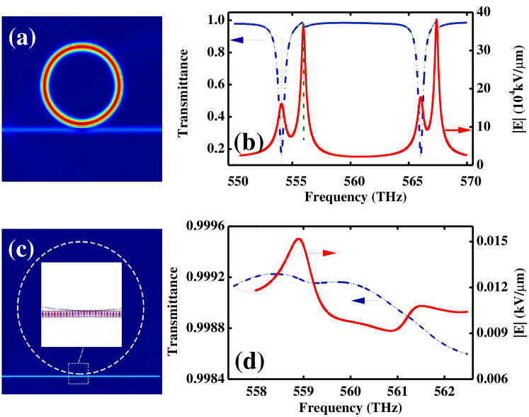
As an example, we started with the conventional coupling between dielectric waveguide and dielectric cavity [16], as shown in Fig. 1(a). Electromagnetic wave with magnetic field perpendicular to the plane constituted by waveguide and cavity (TM mode) is loaded at the left facet of the waveguide. And the input power is , which is actually the linear density of input power, since our simulations are based on two-dimensional model. For single cavity mode, the steady state cavity field and transmitted field can be obtained from the input-output relation [17] as
| (1) |
| (2) |
where and are the field and frequency of input light, , and are frequency, intrinsic loss (including radiation, absorption and scattering losses) and external coupling loss (coupling to the waveguide) of the cavity mode. Figure 1(b) displays the normalized transmission spectrum () of waveguide and the spectrum of normalized cavity field . The transmission spectrum contains symmetric Lorentzian dips and Fano-type line-shapes, which correspond to the peaks appeared in energy spectrum and arise from the coupling of guided mode to the WGMs in microcavity. As shown by the field distribution in Fig. 1(a), energy is effectively coupled into the cavity when on resonance (). The deep dips in transmission spectrum (dotted line in Fig. 1(b)) correspond to the 2nd-order radial mode working near the critical coupling condition (), while the Fano-like transmission (dashed line in Fig. 1(b)) is brought about by the fundamental mode working in the over-coupling regime ().
Afterward, the coupling between dielectric waveguide and metal (silver) resonator is studied, as shown in Fig. 1(c). Here, the input power is about , and the relative permittivity of silver is . The very small imaginary part of , which is possible at low temperature [18], is set to reduce the Ohmic loss of silver and to raise the Q factor of the metal cavity. In contrast to the dielectric cavity case, the transmission spectrum and the energy spectrum for silver cavity coupling do not show obvious resonance, as displayed in Fig. 1(d). The exterior (plasmonic) WGMs can not be excited by the dielectric waveguide efficiently (Fig. 1(c)), since the coupling strength is rather small compared to its intrinsic loss ().
3 Analysis
In order to improve the coupling efficiency between dielectric guided mode and exterior WGMs, we should firstly understand the underlying mechanism of the coupling process. Actually, for the dielectric cavity case, light is well confined in dielectric waveguide and cavity, with only a minor portion of evanescent field overlapped with each other. Based on the perturbation theory, the coupling strength is proportional to the integral of the overlap between their wave functions [19, 20]. However, for metal cavity case, energy of exterior WGMs is mostly distributed outside the cavity. When the waveguide approach the cavity, the field overlap is very large and the field distribution is greatly altered. Thus, the coupling between dielectric guided modes and plasmon mode can no longer be analyzed with perturbation theory.
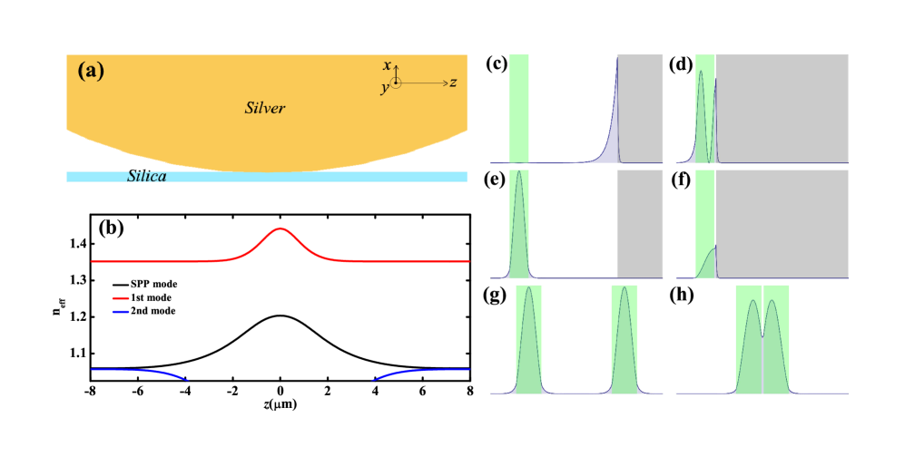
To further analyze the difference therein, we started from solving the hybrid plasmon-dielectric modes with the dielectric waveguide coupled to silver microresonator, the schematic of which is illustrated in Fig. 2(a). Note that, , which determines the cavity mode, is dependent on the energy transfer when waveguide and cavity draw close to each other. Thus, we focus on the coupling region without worrying about the details of cavity. We calculated the effective refractive indices of eigenmodes supported by dielectric waveguide and metal cavity at the cross-section of point , which are related to the gap between waveguide and cavity, as shown in Fig. 2(b). The red and black curves correspond to guided dielectric mode and plasmon mode, respectively. As shown by the electric field profiles of eigenmodes in Figs. 2(c)-(f), both dielectric mode and plasmon mode have been greatly changed due to mode hybridization. When the gap between waveguide and cavity is large, dielectric mode and plasmon mode are independent, and are confined in the waveguide and around the cavity, respectively (Figs. 2(c) and 2(e)). But when the gap minifies, the overlap between dielectric and plasmon modes is so large that the two modes are hybridized and form completely distinct modes (Figs. 2(d) and 2(f)). This point is also reflected in Fig. 2(b): the three eigenmodes evolve to be only two, as the light propagates towards the origin. Hence, this situation differs a lot from the dielectric cavity case, where new normal modes are linear superpositions of the two dielectric modes according to perturbation theory (Figs. 2(g) and 2(h)).
Then, with the of eigenmodes, mode propagation during the coupling region can be obtained. Similar to the time evolution of quantum states, the evolution of modes in the waveguide follows Schrödinger equation [21, 22], and can be expressed as
| (3) |
where is the Hamiltonian as a function of due to the variation of the gap between waveguide and cavity along axis, and is the instantaneous eigenfunction at the point . According to Ref. [23], we obtained the coupling dynamic equations
| (4) |
Here, is the eigenmode of , while is the corresponding coefficient, is the coupling strength between eigenmodes and , and is the propagation constant of the eigenmode. The first term in Eq. 4 is the Berry phase, which does not play a significant role in the coupling process since its integral equals to zero. The second term in Eq. 4 stands for the coupling between eigenmodes (, rather than the eigenmodes of separate waveguides above), which reveals the requirements for efficient mode conversion. The first factor is the coupling strength , another one is the exponent which stands for phase.
Since is dependent on the gap between waveguide and cavity (with the minimum gap denoted as ), can be rewritten as , where . As waveguide approaches the cavity, , with being the cavity radius. The slowly varying gap ( ) and the large mismatching in propagation constant () (Fig. 2(b)) give rise to the adiabatic conversion [24]. That is to say, energy in dielectric waveguide is coupled into metal resonator as plasmon mode, and then is converted back to waveguide as dielectric mode. And the field distribution in Fig. 1(c) has shown that little energy can be coupled into silver cavity with a straight waveguide. Therefore, we need to break the adiabatic mode evolution (1) by engineering to vary faster or (2) by phase matching. It’s worth noting that the breaking adiabatic evolution here is a fast varied process and is essentially different from Landau-Zener transition between different states at the anti-crossing of energy level [25, 26], which still applies to perturbation theory.
Inspired by the analysis above, we proposed two methods that could enhance the coupling from silica waveguide to silver cavity. Firstly, we considered the coupling between silver cavity and a U-shaped bent waveguide [27, 28], the outer radius of which in the semicircle coupling region is . Next, with regard to the exponent factor, the effective refractive index of dielectric mode needs to be reduced to match with plasmon mode. So we investigated the behavior of the second-order dielectric mode in waveguide, as shown by the blue curve in Fig. 2(b), which is pretty close to of plasmon mode in silver cavity. Hence, we can utilize the second-order optical mode in silica waveguide to reach phase matching with the plasmon mode in silver cavity. In the following, we’ll verify our protocols by numerical simulations.
4 Results and discussion
4.1 Bent waveguide coupler
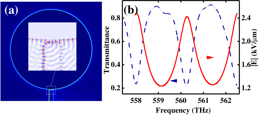
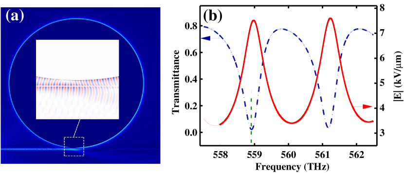
We firstly studied the coupling between a U-shaped bent silica waveguide and silver cavity, with the input power around . As shown in Fig. 3(a), when the input light is on resonance with the cavity mode, most energy is confined around the metal cavity and little is transmitted from dielectric waveguide. This demonstrates the efficient coupling from dielectric waveguide to metal cavity. And the effective coupling originates from the rapidly changed gap , which raises the coupling strength between them and breaks the original adiabatic evolution. Besides, benefiting from the properties of SPPs, energy in cavity is extremely confined in the metal surface with an ultra-small mode volume. The visual impression that coupling has been improved in Fig. 3(a) is further supported by the transmission spectrum of waveguide and the energy spectrum of cavity in Fig. 3(b). Since there is only fundamental exterior plasmon WGMs, the spectrum shows very regular dips and peaks with equal interval. The Q factor of cavity can be calculated from the energy spectrum as , with being the full width at half maximum (FWHM). For the resonance at , we obtained .
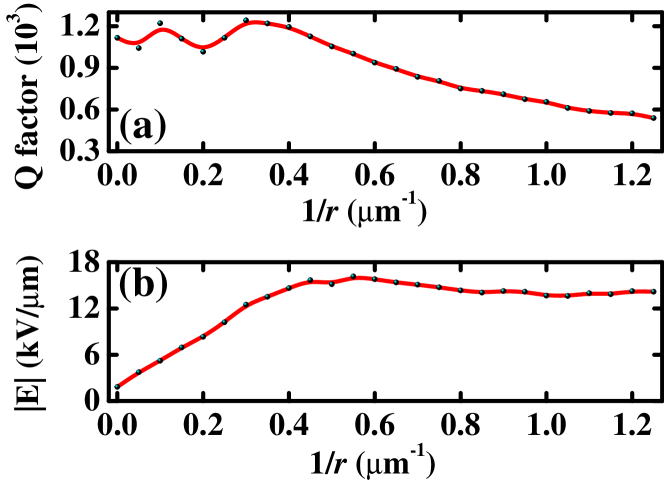
For a better understanding, we calculated the influence of outer radius of waveguide on the dielectric-plasmon coupling. In Fig. 4(a), the dependence of Q factor on is displayed. The zero point where corresponds to a straight waveguide coupling with silver cavity, and the low Q factor which is much lower than that of bare cavity is due to the waveguide induced scattering loss. The increase of leads to that: (1) the adiabatic change of the gap between waveguide and metal cavity is destroyed, (2) the region that waveguide interacts with cavity is reduced. The former effect gives rise to the increase of coupling , as indicated in Fig. 4(b) that cavity energy increases with increasing . The later effect induces complex behavior of cavity loss : as the interaction region is shortened, the waveguide induced scattering loss decreases at first, but very strong scattering loss is induced when the interaction region is comparable to wavelength. At the optimal bent coupler radius , is increased by about one order (Fig. 4(b)).
4.2 Higher-order mode coupler
Excitation with the second-order dielectric mode in a straight waveguide is also investigated, as displayed in Fig. 5(a). TM mode with input power around excites the waveguide at the facet. Here, we study the influence of second-order dielectric mode only, since the mismatching between dielectric fundamental mode and plasmon mode is really large and the inefficient coupling with fundamental mode has been shown in Fig. 1(c). The inset in Fig. 5(a) is the zoom-in view of the coupling between dielectric and plasmon modes, where the second-order mode in silica waveguide is clearly coupled into the silver cavity with minor energy leaked. Similarly, the transmission spectrum of waveguide and the energy spectrum of cavity are also calculated, as shown in Fig. 5(b). The transmission approaching zero at (dashed line in Fig. 5(b)) indicates that the coupling between silica waveguide and silver cavity can even reach critical coupling. And the Q factor of cavity extracted from the energy spectrum is at .

Then, the performance of this coupling protocol dependent on the minimum gap between waveguide and cavity is studied. The dependences of Q factor and energy on are shown in Figs. 6(a) and 6(b) respectively, which are obtained by tracking a specific peak whose eigen-frequency blueshifts with increasing . When , the Q factor and show strange oscillation against . In this regime, the waveguide is very close to the metal, so the dielectric mode is strongly effected by the plasmon mode, leading to complex behavior of the integration in Eq. (4). In addition, of the dielectric mode is close to the refractive index of air, thus the coupling will also induce loss into the leaking modes in air. When keeps on going up (), the overlap between dielectric and plasmon modes is so weak that the perturbative coupled-mode theory can be applied. So, exponentially decreases with increasing , while the cavity intrinsic loss remains constant. At , (Fig. 6(a)) indicates that the external coupling loss is reduced to equal the intrinsic loss , corresponding to a maximum cavity field in Fig. 6(b).
4.3 Discussion
From above results, we see that breaking the adiabatic condition effectively enhances the energy transfer between dielectric waveguide and plasmonic cavity. For the bent coupler, the efficiency is slightly lower than the case of higher-order mode coupling, but with the merits of simple excitation with fundamental mode and compact coupler size. It is well known that the application of plasmon modes is strongly limited by the Ohmic loss, so efficient coupling can be expected by reducing the device size to minimize the loss. Therefore, a bent coupler will be an effective way to excite and collect plasmon modes. For higher-order mode coupling, it shows critical coupling when the waveguide is not very close to the cavity. The achieved cavity field is about 2 times stronger than that for bent coupler. In addition, the result indicates that higher coupling strength can be achieved for smaller gap. That is to say, critical coupling is possible for low-Q exterior WGMs in smaller cavity or cavity with larger metal loss. It’s also shown that the coupling is not very sensitive to the gap, as the field for contact coupling case () is about for the optimal case ().
5 Conclusions
In summary, we study the coupling between dielectric waveguide modes and exterior plasmonic whispering gallery modes, which is quite different from the coupling between dielectric modes. Based on the theoretical analysis of the principle therein, we propose two protocols to strengthen the dielectric-plasmon mode coupling. The first one is to break the adiabatic conversion with a U-shaped bent waveguide, and the other one is to render the dielectric mode of higher-order to reach phase matching with plasmon mode. Through numerical simulations, the validity of our proposals is fully vindicated by the transmission spectra of waveguide and the energy spectra of cavity. Besides, the influencing factors in two schemes are all analyzed in detail. Both of the schemes demonstrate that the coupling efficiency can be greatly raised. The effective coupling between dielectric guided mode and plasmon mode may find various applications for tunable integrated optical devices and bio-sensors.
Acknowledgments
Chen-Guang Xu and Xiao Xiong contribute equally to this article. This work was funded by NBRP (grant nos. 2011CBA00200 and 2011CB921200), the Innovation Funds from the Chinese Academy of Sciences (grant no. 60921091), NNSF (grant nos. 10904137, 10934006 and 11374289), the Fundamental Research Funds for the Central Universities (grant no. WK2470000005), and NCET.