DEPFET active pixel detectors for a future linear collider
Abstract
The DEPFET collaboration develops highly granular, ultra-transparent active pixel detectors for high-performance vertex reconstruction at future collider experiments. The characterization of detector prototypes has proven that the key principle, the integration of a first amplification stage in a detector-grade sensor material, can provide a comfortable signal to noise ratio of over 40 for a sensor thickness of 50-75 . ASICs have been designed and produced to operate a DEPFET pixel detector with the required read-out speed. A complete detector concept is being developed, including solutions for mechanical support, cooling and services. In this paper the status of DEPFET R & D project is reviewed in the light of the requirements of the vertex detector at a future linear collider.
Index Terms:
DEPFET, active pixel sensor, vertex detector, linear collider.I Introduction
Experiments at a future linear collider [1, 2] (LC) requires extremely precise reconstruction of the reaction products to perform precision physics programs to study the electroweak symmetry breaking mechanism and physics beyond the Standard Model. Key figures of merit for the detector performance, such as the jet energy resolution, momentum resolution for charged tracks and the vertexing capabilities of the experiment, must be improved significantly with respect to the state-of-the-art detectors realized in the LHC experiments. A worldwide detector R & D effort is ongoing to fully satisfy the challenging requirements.
Finely segmented solid state detectors are crucial for the reconstruction of the trajectory of charged particles in modern collider experiments. In active pixel detectors the small signal generated when charged particles traverse a thin layer of Silicon is amplified in the sensor itself. Over the last decade an international collaboration has developed the DEPFET (Depleted Field Effect Transistor [3]) concept, where a FET is integrated in the active sensor to amplify the signal. These DEPFET structures present interesting possibilities for a number of applications. The excellent signal to noise (S/N) ratio that can be achieved has led to applications such as space-based X-ray Astronomy missions and X-ray detection in the European XFEL [4]. It also allows for a strong reduction of the material budget of position-sensitive devices for charged particle detection at collider experiments. The proposal of a DEPFET vertex detector for a future linear collider [5, 6] dates back to 2002. The DEPFET collaboration has since shown that finely segmented devices with large in-pixel gain can indeed be constructed and operated. Read-out and control ASICs have been designed and produced, and a novel ladder design with excellent thermo-mechanical properties has been developed. A fully engineered vertex detector design, including all supports and services, is being developed for the Belle II experiment [7].
Recent descriptions of the DEPFET active pixel detector project are found in References [8] and [9]. The Belle II technical design report [7] provides a very complete description of the DEPFET-based vertex detector of that experiment (see also [10, 11]). However, the most recent document reviewing DEPFET progress towards a vertex detector for a linear collider [12] was prepared for the ILC R & D panel in 2007. The present paper aims to fill this gap, reviewing the major milestones of the DEPFET project since then in the light of a linear collider at the energy frontier.
The requirements on an LC vertex detector are briefly summarized in Section II. The DEPFET concept is reviewed in Section III and a ladder design for an LC vertex detector based on DEPFETs is schematically presented in Section IV. The following Sections highlight recent progress in several key areas, such as: sensor production (Section V), ASIC development and performance (Section VI), and power consumption and cooling (Section VII). In Section VIII results from the characterization of prototypes are presented. The results are summarized in Section IX.
II Requirements on an LC vertex detector
Detector concept studies for future linear colliders have established a number of challenging performance goals based on the analysis of benchmark channels and an evaluation of the LC environment [2, 13, 14, 15, 16].
The first layer of the LC vertex detector must cope with large irreducible backgrounds due to incoherent pair production. Long bunch trains are envisaged in the ILC Technical Design Report, with 1312 bunches separated by 554 ns 111These numbers have changed with respect to the LOI, that contemplated 2820 bunches with 337 ns spacing. However, these changes are accompanied by a factor two increase in bunch current, such that the background hit density per unit area and unit time remains virtually unaltered.. A background hit density of up to 10 hits in the innermost layers of the ILC vertex detector at 15 mm from the interaction point require read out times of 50-100 and a highly granular detector [13, 14].
The background hit rates scale approximately with the instantaneous luminosity, which is in turn expected to increase proportionally with the center-of-mass energy of the machine. The read-out speed requirements are therefore considerably more relaxed in the early low-energy stage (at 250 350 GeV) than in the nominal 500 GeV stage and in the envisaged 1 TeV upgrade. CLIC envisages shorter trains of order 300 bunches with a 0.5 ns spacing. Time stamping of single bunches in this environment requires devices with a read-out speed beyond the current state of the art, a challenge that is not addressed in this Transaction.
The aim for the vertexing capabilities of the LC detectors is often summarized with the following requirement on the impact parameter resolution222The value of the material term is increased from 10 to 15 in the CLIC requirement as a consequence of the increased inner radius. :
| (1) |
This goal respresent a considerable improvement over vertex detectors built at collider experiments to date; the constant term is better by a factor 2-4 than what was achieved at previous colliders and at the LHC. Achieving the requirement for the second (material) term is even more challenging; it has to decrease by a factor 6-10 with respect to most previous experiments333The best material term so far was achieved by the SLD vertex detector with . This CCD based detector had 0.36% of a radiation length per layer.. Indeed, the requirement in Formula 1 (together with the assumed inner radius of 15 mm) implies that the vertex detector must be built with a strict material budget of order 0.1% of a radiation length per layer, roughly equivalent to 100 of Silicon.
To comply with the strict material budget, the detector concepts aim to keep the (average) power consumption below 10 W for the entire vertex detector. With such a low power density (approximately 100 ) no active cooling circuits are required. The key to achieve this goal is the bunch structure of the LC machines. The 0.7 ms long bunch trains at the ILC are separated by intervals of 200 ms. In a pulsed power scheme, where the detector power supply follows the machine duty cycle as closely as possible, a reduction of the average power consumption by a factor of (at maximum) 1/275 is possible. The CLIC bunch trains, with a length of just 156 ns, are separated by 20 ms.
The detectors must be operated in a strong magnetic field, ranging from 3.5 to 5 Tesla in the different detector concepts. The radiation levels in the innermost part of the tracker volume of an LC detector are relatively low compared to the LHC. The non-ionizing dose is of the order of , while the ionizing radiation amounts to less than kGy per year [13, 2].
III The Depleted Field Effect Transistor
A brief introduction of the Depleted Field Effect Transistor is presented in the following. For a complete discussion the reader is referred to more detailed descriptions elsewhere [7, 12].
A schematic view of the DEPFET concept is shown in Figure 1. A Field Effect Transistor (FET) is embedded in detector-grade Silicon. An electric field is set up in the sensor to deplete it of free charge carriers and to ensure fast signal collection with limited diffusion. The signal is collected on the internal gate, an implant immediately below the FET, where it modulates the drain current. After read-out the collected signal is removed from the internal gate by applying a voltage pulse to the clear contact.
With this structure a first amplification of the signal is achieved, that allows to reduce the active detector thickness to several tens of microns while maintaining a comfortable S/N ratio for minimum ionizing particles (MIPs). The gain of this first stage (expressed in units of current per electron) is one of the crucial parameters of the DEPFET.
IV DEPFET active pixel detectors
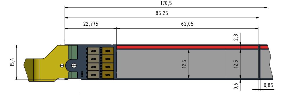
A finely segmented active pixel sensor is achieved by introducing a matrix of very small DEPFET structures on the surface of the sensor. A schematic of a DEPFET ladder for the innermost layer of an LC vertex detector is depicted in Figure 2. The matrix of pixels is read out in a rolling shutter architecture. Control ASICs located on a narrow balcony that stretches along the length of the ladder address subsequent rows of pixels. Each column composed of approximately 1000 DEPFET pixels is read out by a single channel of a read-out chip located at the end of the sensor. As the shutter rolls over the matrix, each row of pixels444In practice, two or four rows are read out in parallel to reduce the time required to read out a complete frame. is switched on in turn. The frame time needed to read out the complete matrix is then given by the depth of the column multiplied by the time required to read out a single pixel. The auxiliary ASICs required to operate and read out the DEPFET sensors are discussed in more detail in Section VI
To comply with the very tight material budget the sensor must be thinned and the material in support and services must be reduced to the bare minimum. The all-Silicon concept aims to achieve both by integrating active material, support structures and the high-density interconnect in a self-supporting ladder [17, 18].
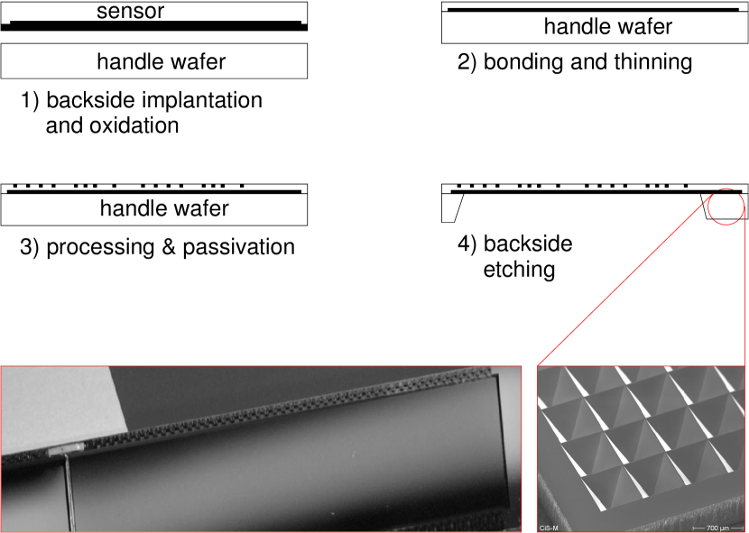
The most important process steps are illustrated in Figure 3. In the first step the backside implants are placed and the sensor wafer is oxidized. In the second step the sensor wafer is bonded to a thick handle wafer; the sensor is ground to a thickness of 50 (75 for Belle II). In the third step the DEPFET processing is performed on the front side. Through a final photolithographic step (deep anisotropic etching) windows are opened in the second (support) wafer below the sensitive part of the sensor. The thicker Silicon around the edges of the sensor forms a support frame. A photo of the resulting ladder is shown in the same Figure. The material in the edges is further reduced in the same lithography step by introducing grooves. With the etching technique used complex structures can be produced. A good example is shown in Figure 3, that presents a scanning electron microscope image of an edge produced with this technique. The all-Silicon ladders have excellent mechanical properties. The all-Silicon mechanical concept is fully self-supporting and requires no external support structure over the length of the ladder. The use of a single material furthermore reduces the mechanical stress due to mismatching of thermal coefficients.
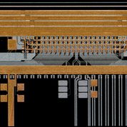
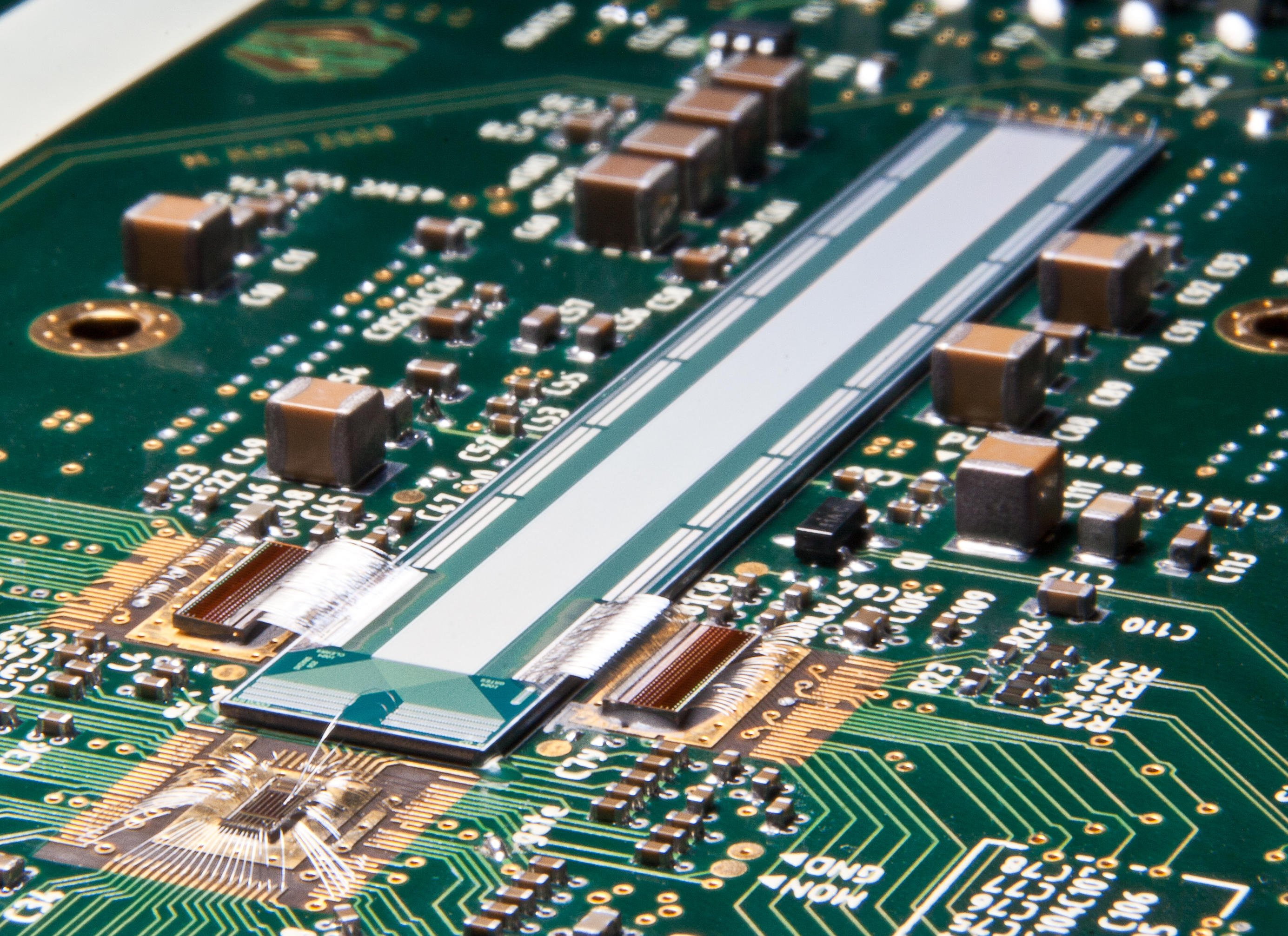
Auxiliary detector components such as the control and read-out ASICs are integrated onto the sensor using bump-bonding. Power and signal lines are routed on an additional metal layer on the sensor, thus obviating the need for a separate high-density interconnect cable. A close-up image of part of the high-density interconnections on a Belle II ladder is shown in Figure 4.
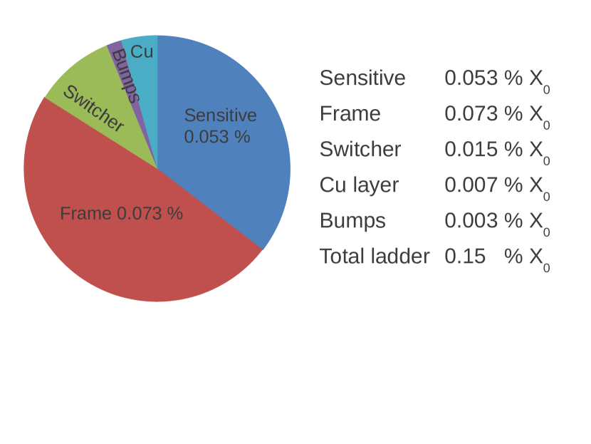
The detailed ladder design for an LC vertex detector envisages a contribution to the detector material (averaged over the ladder area) that is equivalent to % X0/layer. A break-down of the material among the components with the most important contributions is presented in Figure 5. The fully engineered Belle II design [7] corresponds to % X0/layer over the active area. The LC budget is reduced primarily by a more aggressive thinning of the sensor. The thickness of the active material, one of the dominant contributions, is reduced from 75 to 50 (as already achieved in the Belle II prototype production run). The support frame is reduced from 450 to 400 .
V Sensor production
The DEPFET pixel technology contains 25 photolithographic mask steps and nine implantations. The process involves moreover very different technology aggregates like wafer bonding, Silicon-on-Insulator (SOI), double poly Silicon, triple metal (including copper), back side thinning and double sided wafer processing. All processing steps except the SOI production are performed in-house.
Two early sensor production batches have proven the feasibility of small pixels down to 20 20 . The performance of the ILC prototypes constructed with these sensors is described in several previous publications [19, 20].
The more recent Belle II prototype production run (“PXD6”) was performed on an SOI wafer and all matrices were thinned to 50 . Sensor designs with large pixels (50 50 and 50 75 ) for Belle II were added to the mask, as well as further design variations of the pixel layout. The results of a characterization of these sensors are presented in Section VIII.
Based on the results and experiences of “PXD6” prototyping, the production run for Belle II (“PXD9”) has started. Apart from some other, minor modifications, the gate and clear-gate dielectrics are reduced to 100 nm, approximately half the thickness used previously, for better radiation hardness555The Belle II environment, with an expected ionizing dose of 18.5 , exposes the sensors to significantly higher radiation levels than that at the ILC, where the required tolerance amounts to approximately 1 kGy/year [21]. . This leads to a reduction of the internal gain, that scales approximately with the square root of the oxide thickness. The performance is partially recovered by modifying other parameters of the FET layout. The gain depends strongly on the gate length () and in the longer term a considerable increase of the improvement can be achieved by reducing the gate dimension. A more detailed discussion of the dependence of the gain is left for Section VIII).
VI Control and read-out ASICs
Several auxiliary ASICs are required to operate the DEPFET sensor. The most important developments are briefly summarized in this Section.
The SWITCHER control chips select segments of the sensor (pairs of rows or 4-row segments) for read-out. A separate driver supplies the clear pulse of up to 20 V to remove the collected signal from the internal gate after read-out.
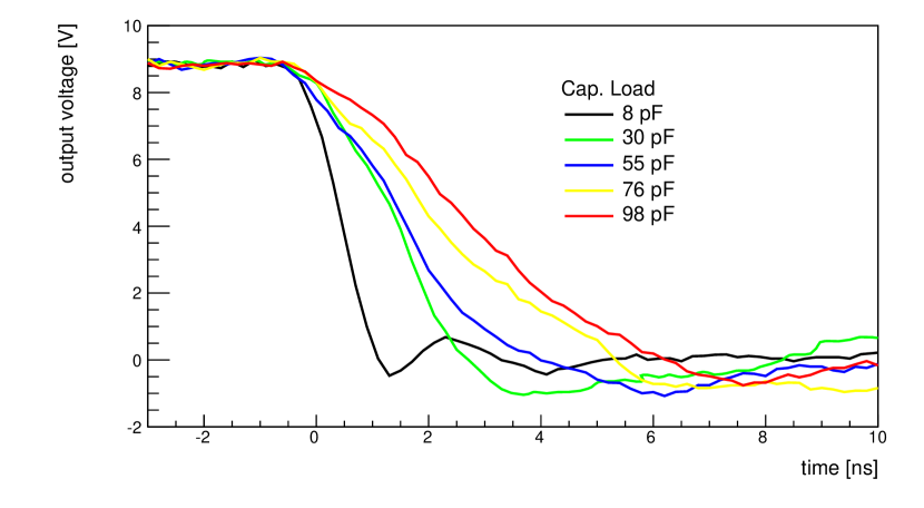
Two designs of the SWITCHER versions optimized for Belle II requirements (SWITCHERB18 in 0.18 and SWITCHERB in 0.35 ) have been produced and tested successfully. The radiation hardness of the 0.35 design is demonstrated up to 370 kGy. The 0.18 version is smaller, allows for faster switching, lower power consumption and is expected to improve the radiation tolerance. It can produce pulses with a maximum swing of 20 V in a voltage range of 50 V. The falling edges under different load conditions of 9 V pulses generated by SWITCHERB18 are presented in Figure 6. These measurements show that the current SWITCHER chips can drive long lines, up to loads well beyond the requirements of the Belle II and LC vertex detectors.
The drain current signals from 256 columns of pixels are processed and digitized by the DCD (Drain Current Digitizer [22, 23, 24, 25]) chip. The analog input stage keeps the column line potential constant (necessary to achieve fast readout), compensates for variations in the DEPFET pedestal currents, and amplifies and shapes the signal. The current receivers in the most recent DCD versions are based on transimpedance amplifiers (replacing the regulated cascodes of earlier generations). The analog signal is digitized using two 8-bit current-mode cyclic ADCs with a sampling frequency of 10 MSamples/s. The DCD can be operated in double correlated sampling mode or single sampling mode. The latter is preferred as it allows higher read-out speed.
The DCD is implemented in UMC 0.18 CMOS technology using special radiation hard design techniques (e.g. enclosed NMOS gates) in the analog part. The 256-channel DCDB, with an area of 3.2 5 , is optimized specifically for Belle II requirements. The DCDB chip is fully functional at the nominal 320 MHz. Radiation tolerance of at least 70 kGy has been proven.
The derandomized raw data from the DCD are transmitted to the Data Handling Processors (DHP [26]) using fast parallel 8-bit digital outputs. This third ASIC, located on the end-of-ladder area immediately behind the DCD, performs data processing (pedestal subtraction, common code correction), compression (zero suppression), buffering and fast serialization. It furthermore controls the other read-out ASICs.
The first full-scale DHP prototype was implemented in IBM 90 nm CMOS technology. Communication of the DHP chip with the other ASICs has been successfully tested. Implementation of the next DHP version is foreseen in TSMC 65 nm CMOS technology. In the longer term the DCD and DHP are envisaged to evolve into a single chip.
The analog stage of the DCD is most important for the detector performance. The analog response has been characterized in detail [25, 27] on the test system of Figure 7 where a DCD2 and SWITCHER are connected to a full-size DEPFET sensor.
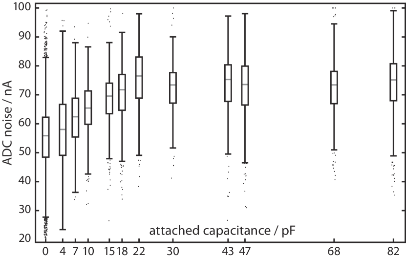
The ADC conversion factor is found to be approximately 10.2 , with a slight dependence on the read-out speed and the analog supply voltage, with a channel-to-channel variation of less than 0.2 [27]. In the upper panel of Figure 8 noise measurements for several values of the capacitative load on the input stage are presented. We find a DCD noise of approximately 80 for the load of a full-length DEPFET ladder (about 80 ).
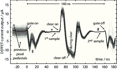
The read-out speed is one of the most challenging requirements of the LC vertex detector. The sequence involved in the read-out of one row in single-sampling mode is illustrated in the lower panel of Figure 8. The drain current is found to settle approximately 30 ns after the row is activated (indicated as “gate on” in the figure). After the current is sampled the clear pulse is applied. Thus a row rate of approximately ns is achieved. Figure 8 clearly shows that there is ample room for improvement. A further increase of the read-out speed, with row rates down to ns, requires a number of changes to the design of the read-out ASIC.
To interprete this result in the LC perspective we consider the following layout: the 12.5 cm long inner layer of the ILC VXD is equipped with a DEPFET sensor with read-out ASICs on both ends. Pixels in the center of the sensor are 25 25 . The pixel size is varied over the length of the sensor, ensuring that charge is shared over a small number of pixels independent of the z-position. The pitch is increased to 50 at 1 cm and to 100 at 2 cm. With a column depth of 1025 pixels per half-ladder, and two (four) rows sampled in parallel, the envisaged row rate of ns implies a read-out time for a complete frame of 40 (20 ).
VII Power consumption & Cooling concept
The strict material budget of the LC vertex detector forces a tight control of the power consumption. The DEPFET sensor with rolling shutter read-out are intrinsically well suited to this environment, as its power consumption scales with the number of pixels addressed in parallel (i.e. the number of read-out columns), rather than with the number of pixels. In the DEPFET sensor, the signal is collected in the internal gate regardless of the gate voltage supplied to the FET. The FETs only need to be powered during the brief lapse of time when the drain current is read out. Only a small fraction of rows is therefore active at any time during operation. All other pixels are switched off and draw no current. Other sources, such as the leakage current are negligible even after irradiation.
For the layout sketched in Section VI, and assuming 2-fold (4-fold) read-out only 0.2% (0.4%) of pixels are active at any time during operation. The instantaneous power consumption of a half ladder is therefore given by:
where is the drain current, is the source-drain voltage, the number of columns in the sensor and the number of rows read out in parallel. The estimate given corresponds to the situation where two rows are read out in parallel. For four-row read-out the power consumption in the sensor is doubled.
The power consumption required to drive the gate and clear lines is dominated by the SWITCHERs that consume 225 per active row. The consumption of each active chip is 50 mW and idle chips contribute 10 each. With two active rows per half ladder at any time during operation the power consumption is approximately 500 per half ladder.
The current consumption of the 256-channel DCD is measured to be 1.3 W. Most power is dissipated in the analog input stage that requires up to 3 channel to ensure fast read-out with good noise performance. The DHP implemented in a 90 nm process is found to consume less than 200 mW. Four DCDs and four DHPs are required to read out a half-ladder, leading to a local power consumption at each end of the ladder of 6 W.
With 8 short and narrow inner ladders in layer 1 and 56 wider and longer outer ladders in layers 2 through 5, the total instantaneous power required to operate a DEPFET vertex detector at the ILC is approximately 1 kW. Note that these results, based on the measured consumption of complete ASICs, are slightly better than the conservative estimate in 2007 [12].
The LC duty cycle of 1/275 is the key to reduce the average power consumption of the detector further. The power pulsing scheme pursued by most LC detectors is implemented in DEPFET sensors for XFEL, where the DEPFET and the analogue part of the electronics are switched off between bursts. Taking an effective detector duty cycle of 1/100 the average power consumption of the vertex detector can be kept below 10 W.
The DEPFET cooling concept was developed on the basis of a detailed finite element model [28] of the read-out module. For crucial parameters the simulation is cross-checked against measurements on test structures. As the Belle II vertex detector relies on a forced flow of dry and cold gas to reduce the temperature of the center of the ladder, the potential of gas cooling was studied with special care. To predict the temperature in the LC the same model is adapted.
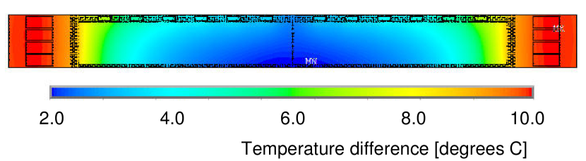
The power consumption of the different detector components is as described above, leading to a total instantaneous power consumption of 600 W. The average power is taken as of the instantaneous consumption to account for the impact of pulsed powering. A gas flow of 2 is forced on both sides of the ladder. The expected temperature distribution for the innermost LC ladder is shown in Figure 9. The end-of-ladder with the read-out electronics reaches a temperature 10∘ C above that of the cold gas, while the center of the sensor stays within two degrees of the gas temperature.
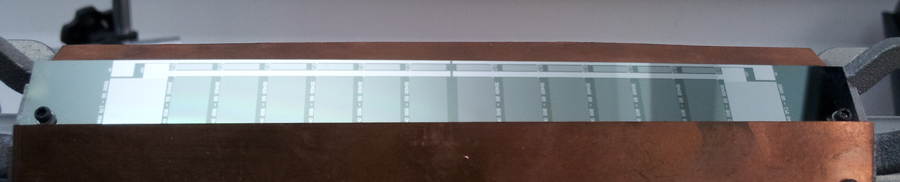
The understanding of the thermal properties of the ladder is greatly enhanced by measurements on the thermo-mechanical samples shown in Figure 10. These are mechanically identical to DEPFET all-Silicon ladders, but lack some of the processing steps needed to turn them into fully functional sensors. Small circuits on the relevant positions allow to mimic the power consumption of the ASICs and the sensor. The power dissipated in each circuit can be regulated independently.
Using thermo-mechanical samples a mock-up has been built that represents the first two layers of the vertex detector [29, 30]. The mock-up is equipped with a system to provide a gas flow of controlled rate, temperature and humidity. Measurements of the temperature distribution with a thermal camera and an environmental monitoring system based on Bragg fibers [31] confirm the predictions of the finite element model.
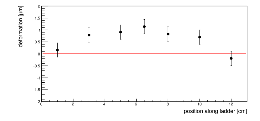
Capacitative sensors are used to monitor the position of the ladder without distorting the system. Upon application of the gas flow the ladder position is slightly distorted. The maximum deformation is registered at the center of the sensor: the measured -coordinate changes by 1.1 0.3 when the gas flow is switched on. No significant hysteresis is observed; the original ladder position is recovered when the gas flow is switched off. Vibrations introduced by the gas flow are detected by performing position measurements with and without gas flow and taking the difference of the Fast Fourier Transforms of both time series. A clear peak at 400 is observed with an amplitude of 1.2 (0.7 ) for a gas pressure of 10 bar (4 bar). The magnitude of the static and dynamic deformations of 1-2 perpendicular to the ladder have a negligible impact on the resolution of the vertex detector.
VIII Characterization of prototypes
The response of DEPFET sensors from the PXD5 and PXD6 production has been characterized in beams of charged particles from accelerators at CERN and DESY [19, 20, 32, 33]. In the following only some highlights from this extensive program are presented.
The first set of measurements is on 450 ILC-design sensors with pixel sizes ranging from 20 20 to 24 32 . The read-out module for these prototypes relies on the CURO chip [34, 35]. More recent measurements correspond to thinned PXD6 sensors with DCDB read-out.
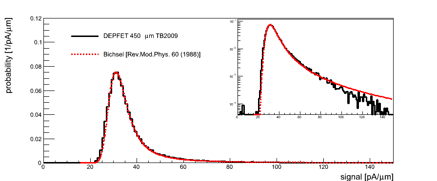

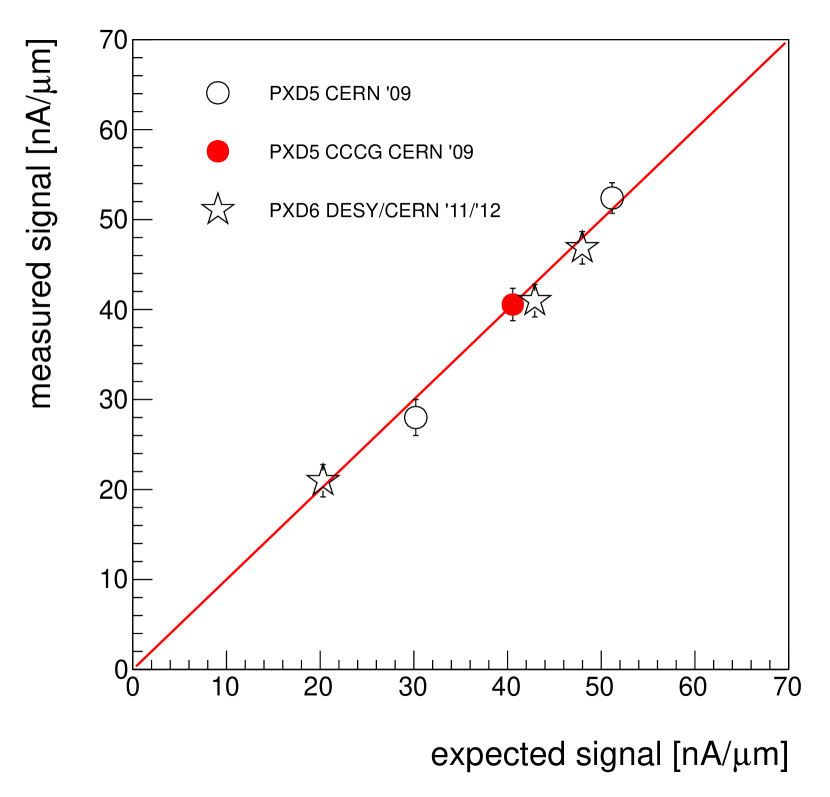
The DEPFET drain current distributions due to perpendicularly incident 120 GeV pions from the CERN SPS are shown in Figure 12. The upper panel corresponds to a 450 thick “PXD5” sensor and the lower panel to a PXD6 sensor thinned to 50 . The signal in adjacent pixels is added using a simple clustering algorithm with a neighbor cut of 2.6 . Further details of the analysis can be found in References [37, 38]. Both measurements are corrected for the gain of the Front End ASICs666The gain measurement for the DCDB is presented in Section VI. For the CURO system used to read out the thick sensor a conversion factor of 7.7 nA/LSB is used [39].. To facilitate comparison the results are moreover divided by the sensor thickness.
The observed distributions are in good agreement with the model prediction of H. Bichsel [36], where only the internal gain of the sensors is left floating. In particular, the model correctly predicts the broader signal distribution observed for the thin sensor: The peak position divided by the Full Width at Half Maximum (FWHM) yields: 1.67 for the 50 sensor (prediction: 1.61) and 3.06 for the 450 thick sensor (prediction: 3.13).
The gain of the in-pixel amplification stage depends on the layout of the FET, in particular on the length of the gate , its width and the oxide thickness , and on the drain-source current . A simple 2D model predicts the following relation:
| (2) |
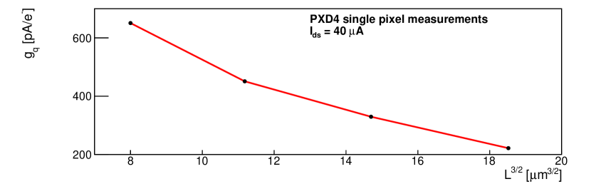
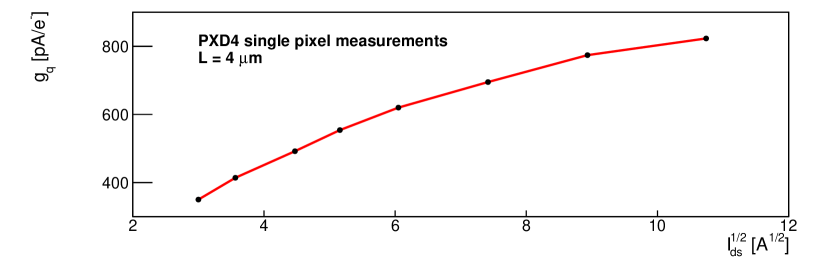
Examples of single-pixel gain measurements from Reference [40, 41] are shown in Figure 13. The response of the complete matrices is compared to the prediction of the model in Figure 14. The measurements on a large number of small-scale structures [40, 41] are also drawn. Clearly, the simple 2D model is insufficient to correctly predict the dependence. In particular, the assumption of constant carrier mobility is known to fail for very large drain current. With some caution as to the range of applicability the model provides, however, an adequate set of rules of thumbs.
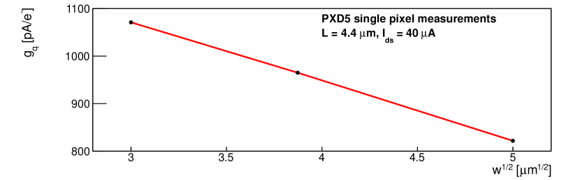
The uniformity of the signal over the area of the sensor has been evaluated as well. In a PXD5 device with approx. 8000 pixels and a 4 gate length a gain spread of 5% 3% is observed. A more recent device with a 5 gate length shows an even more uniform response (random gain spread 3%), but has a systematic difference of 5% between even and odd rows of the device. The cause of this effect is currently being investigated. Variations at this level have a negligible impact on the overall detector performance.
Charge sharing between adjacent pixels is well understood. For typical operating parameters and perpendicularly incident particles the signal in the thin sensors is contained in an area with a diameter of several tens of microns. In sensors with large pixels (5075 ) an extra drift ring is inserted into each pixel to ensure rapid and efficient charge collection.
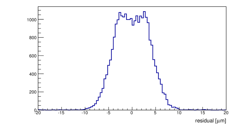
The spatial resolution of DEPFET devices has been studied in detail. Thick DEPFET sensors with an ILC pixel design (thickness pixel size of 450 20 20 ) approach a 1 resolution in both coordinates [42, 19, 20]. The thin Belle II design sensors with 50 50 75 pixels yield a spatial resolution of 8 [38] for perpendicularly incident tracks, in good agreement with the expected performance. Using an extensive set of beam test results on both types of devices, a detailed model of the DEPFET response has been developed for use in simulations of the overall detector performance. This digitizer model is used to predict the spatial resolution of an LC-design DEPFET sensor with a detector thickness of 50 . For comparison to beam test results we consider high-energy charged pions traversing the sensor under a 90 degree incidence angle in the residual distribution of Figure 15. For a DEPFET device with 20 20 (25 25 ) pixels on a 50 thick sensor a spatial resolution of 3.5 (4.5) is found. In more realistic conditions the performance is expected to be significantly better than that. Most tracks traverse the sensor under an angle and deposit signal in multiple pixels. The large magnetic field moreover causes the charge carriers to drift to the read-out plane under an angle (the Lorentz angle). Charge sharing between neighbouring pixels leads to a significant improvement in the spatial resolution.
IX Summary
Future colliders require vertex detectors that combine an excellent spatial resolution and challenging read-out speed with a very tight material budget. The Depleted Field Effect Transistor (DEPFET) offers a promising way to address these challenges. A matrix of DEPFETs embedded in a detector-grade Silicon sensor forms an active pixel sensor with competitive characteristics. A novel thinning concept [43, 44], known as the all-Silicon ladder, allows to produce self-supporting ladders with a minimal material budget ( 0.15% /ladder averaged over the ladder area for an LC vertex detector).
The DEPFET collaboration has succesfully produced small-pixel sensors (down to 20 20 ) and thinned sensors to 50 thickness. The design of the Belle II sensors is frozen and the production of sensors for that experiment has been started. The control and read-out ASICs required to operate the sensor have been produced and are found to meet the LC specifications for read-out speed and noise performance.
The power consumption in the DEPFET sensors with rolling shutter read-out scales with the number of pixels read out in parallel. An estimate for a DEPFET vertex detector at the LC, based on the measured consumption of the current generation of read-out and control ASICs, yields an instantaneous power consumption of a kW. Assuming a duty cycle of 1/100 the average consumption corresponds to only 10 W. Finite element simulations and measurements on a mock-up equipped with thermo-mechanical dummy sensors show that a forced flow of cold gas is very effective in removing the heat from the system, while causing negligible deformations of the ladder.
Prototypes based on thin Belle II design sensors equipped with the ASICs to be used in the experiment have been subjected to an extensive test program. The response to minimum ionizing particles matches closely with the expectation. The dependence of the in-pixel gain on the FET design parameters (gate dimensions and oxide thickness) is found to agree approximately with a naive 2D model. These result show that extremely thin DEPFET ladders (down to 50 ) can achieve a comfortable S/N ratio of over 40. A detailed model of the DEPFET response that provides and adequate description of the signal cluster properties and spatial resolution of the prototypes submitted to beam tests, are used to predict a spatial resolution of 3.5 4 for perpendicularly incident MIPs on an LC design DEPFET device.
We believe, therefore, that the DEPFET sensor technology can fulfill the requirements for a pixel detector in a future LC experiment.
Acknowledgments
The authors would like to acknowledge the support from the AIDA project, that provided the infrastructure used to characterize the DEPFET prototypes in beam tests at CERN and DESY. We also thank Theresa Obermann for her help.
We furthermore thank Hans Bichsel for access to the predictions of his model and him and the authors of GEANT4 for the interesting discussion on the expected signal.
This work was supported by the German Ministerium für Bildung, Wissenschaft, Forschung und Technologie (BMBF), by the Ministry of Education, Youth and Sports of the Czech Republic and by the Spanish Ministerio de Ciencia e Inovación. Marcel Vos is supported by the Spanish Ramón y Cajal program.
![[Uncaptioned image]](/html/1212.2160/assets/x12.jpg) |
Marcel Vos is a researcher of the Spanish research council CSIC funded under the Ramón y Cajal program. He is based at the Instituto de Física Corpuscular (IFIC, UVEG/CSIC) in Valencia, where he works on instrumentation for future collider experiments and searches for signatures of physics beyond the Standard Model in top quark production at the LHC. |
References
- [1] A. Djouadi et al., Eds., International Linear Collider Reference Design Report Volume 2: Physics at the ILC, 2007, ILC-REPORT-2007-001.
- [2] CLIC collaboration, The CLIC CDR, L. Linssen et al., Eds., 2012.
- [3] J. Kemmer and G. Lutz, “New detector concepts,” Nucl. Instrum. Meth., vol. A253, pp. 365–377, 1987.
- [4] G. Lutz et al., “DEPFET-detectors: New developments,” Nucl. Instrum. Meth., vol. A572, pp. 311–315, 2007.
- [5] R. H. Richter et al., “Design and technology of DEPFET pixel sensors for linear collider applications,” Nucl. Instrum. Meth., vol. A511, pp. 250–256, 2003.
- [6] P. Fischer et al., “A DEPFET based pixel vertex detector for the detector at TESLA,” lC-DET-2002-004.
- [7] Abe, T. and others, “Belle II Technical Design Report,” arXiv:1011.0352, 2010.
- [8] M. Vos et al., “DEPFET active pixel detectors,” PoS, vol. VERTEX2009, p. 015, 2009.
- [9] H.-G. Moser et al., “DEPFET active pixel sensors,” PoS, vol. VERTEX2007, p. 022, 2007.
- [10] F. Simon et al., “The Belle-II Pixel Vertex Detector at the SuperKEKB Flavor Factory,” Conf.Proc., vol. C0908171, pp. 563–565, 2009.
- [11] Z. Dolezal, “Super KEKB and Belle II: Status of the KEK Super B Factory,” PoS, vol. EPS-HEP2009, p. 143, 2009.
- [12] L. Andricek et al., “DEPFET Pixel Vertex Detector for the ILC, report of the DEPFET collaboration,” ILC VXD Review, October 22-27, 2007, FNAL, USA, vol. http:aldebaran.hll.mpg.detwikipubDepfetInternalPrc ReviewsDEPFET-Report.pdf.
- [13] ILD concept group, The International Large Detector: Letter of Intent, 2009, DESY 2009-87, Fermilab-Pub-09-682-E, KEK report 2009-6.
- [14] H. Aihara, P. Burrows, and M. Oreglia, Eds., SiD Letter of Intent, 2009, SLAC-R-944.
- [15] T. Behnke et al., Eds., International Linear Collider Reference Design Report Volume 4: Detectors, 2007, iLC-REPORT-2007-001.
- [16] T. Behnke, S. Bertolucci, R. D. Heuer, and R. Settles, Eds., TESLA: The superconducting electron positron linear collider with an integrated X-ray laser laboratory. Technical Design Report. Pt. 4: A detector for TESLA, 2001, DESY-01-011.
- [17] L. Andricek, G. Lutz, R. H. Richter, and M. Reiche, “Processing of ultra-thin silicon sensors for future e+ e- linear collider experiments,” IEEE Trans.Nucl.Sci., vol. 51, pp. 1117–1120, 2004.
- [18] P. Fischer, L. Andricek, S. Herrmann, M. Karagounis, R. Kohrs et al., “Progress towards a large area, thin DEPFET detector module,” Nucl.Instrum.Meth., vol. A582, pp. 843–848, 2007.
- [19] L. Andricek et al., “Spatial resolution analysis of micron resolution silicon pixel detectors based on beam and laser tests,” Nucl. Instrum. Meth., vol. A604, pp. 385–389, 2009.
- [20] J. J. Velthuis et al., “A DEPFET based beam telescope with submicron precision capability,” IEEE Trans. Nucl. Sci., vol. 55, pp. 662–666, 2008.
- [21] ILD concept group, The International Large Detector: Detailed Baseline Design, 2012, to be published.
- [22] J. Knopf, P. Fischer, C. Kreidl, and I. Peric, “A 256 channel 8-Bit current digitizer ASIC for the Belle-II PXD,” JINST, vol. 6, p. C01085, 2011.
- [23] I. Peric, T. Armbruster, M. Koch, C. Kreidl, and P. Fischer, “DCD: The multi-channel current-mode ADC chip for the readout of DEPFET pixel detectors,” IEEE Trans.Nucl.Sci., vol. 57, pp. 743–753, 2010.
- [24] I. Peric et al., “DCDB and SWITCHERB, the Readout ASICs for Belle II DEPFET Pixel Detector,” IEEE Nucl. Sci. Symposium Conference Record N31-5, pp. 1536-1539, 2011.
- [25] J. Knopf, “Development, Characterization and Operation of the DCDB, the Front-End Readout Chip for the Pixel Vertex Detector of the Future BELLE-II Experiment,” Ph.D. dissertation, Ruperto-Carola University of Heidelberg, 2009.
- [26] M. Lemarenko, M. Havranek, T. Hemperek, T. Kishishita, H. Kruger et al., “The data handling processor for the Belle II pixel vertex detector: Efficiency optimization,” JINST, vol. 7, p. C01069, 2012.
- [27] M. Koch, “Development of a Test Environment for the Characterization of the Current Digitizer Chip DCD2 and the DEPFET Pixel System for the Belle II Experiment at SuperKEKB,” Ph.D. dissertation, Ph.D. thesis Bonn University, 2011.
- [28] C. Marinas, “DEPFET: A silicon pixel detector for future colliders. Fundamentals, characterization and performance.” Ph.D. dissertation, Ph.D. thesis Valencia University, CERN-THESIS-2011-101, 2011.
- [29] A. Oyanguren, “Air cooling for vertex detectors.” arXiv:1202.6239v1 [physics.ins-det], 2012.
- [30] P. Ruiz, “Thermomechanical characterization of the Belle II Pixel detector (PXD),” Master’s thesis, Universitat de Valencia, Valencia, 2012.
- [31] D. Moya and I. Vila, “Structural and environmental monitoring of tracker and vertex systems using Fiber Optic Sensors,” 2012.
- [32] L. Reuen et al., “Performance of a DEPFET prototype module for the ILC vertex detector,” IEEE Trans. Nucl. Sci., vol. 53, pp. 1719–1725, 2006.
- [33] R. Kohrs et al., “First test beam results on DEPFET pixels for the ILC,” Nucl. Instrum. Meth., vol. A565, pp. 172–177, 2006.
- [34] R. Kohrs et al., “Development of a prototype module for a DEPFET pixel vertex detector for a linear collider,” IEEE Trans. Nucl. Sci., vol. 52, pp. 1171–1175, 2005.
- [35] M. Trimpl, “Design of a current based readout chip and development of a DEPFET pixel prototype system for the ILC vertex detector,” Ph.D. dissertation, Bonn University, Germany, 2005.
- [36] H. Bichsel, “Straggling in thin silicon detectors,” Rev. Mod. Phys., vol. 60, no. 3, pp. 663–699, Jul 1988.
- [37] B. S. et al., “Beam tests of thin depfet prototypes,” To be published, 2012.
- [38] M. Boronat Arévalo, “The spatial resolution of DEPFET active pixel detectors,” Master’s thesis, Universitat de Valencia, Valencia, 2012.
- [39] R. Kohrs, “Development and characterization of a DEPFET prototype system for the ILC vertex detector,” Ph.D. dissertation, Bonn University, Germany, 2008.
- [40] L. Andricek, P. Kodys, C. Koffmane, J. Ninkovic, C. Oswald et al., “Advanced testing of the DEPFET minimatrix particle detector,” JINST, vol. 7, p. C01101, 2012.
- [41] S. Rummel, “Investigation of DEPFET as Vertex Detector at ILC - Intrinsic properties, radiation hardness and alternative readout schemes,” Ph.D. dissertation, Technische Universitaet Muenchen, 2009.
- [42] L. Andricek, J. Caride, Z. Dolezal, Z. Drasal, S. Esch et al., “Intrinsic resolutions of DEPFET detector prototypes measured at beam tests,” Nucl.Instrum.Meth., vol. A638, pp. 24–32, 2011.
- [43] H.-G. Moser, L. Andricek, R. H. Richter, and G. Liemann, “Thinned silicon detectors,” PoS, vol. VERTEX2007, p. 013, 2007.
- [44] L. Andricek, G. Lutz, R. H. Richter, and M. Reiche, “Processing of ultra-thin silicon sensors for future e+ e- linear collider experiments,” IEEE Trans. Nucl. Sci., vol. 51, pp. 1117–1120, 2004.