Effects of optical and surface polar phonons on the optical conductivity of doped graphene
Abstract
Using the Kubo linear response formalism, we study the effects of intrinsic graphene optical and surface polar phonons (SPPs) on the optical conductivity of doped graphene. We find that inelastic electron-phonon scattering contributes significantly to the phonon-assisted absorption in the optical gap. At room temperature, this midgap absorption can be as large as 20-25% of the universal ac conductivity for graphene on polar substrates (such as Al2O3 or HfO2) due to strong electron-SPP coupling. The midgap absorption, moreover, strongly depends on the substrates and doping levels used. With increasing temperature, the midgap absorption increases, while the Drude peak, on the other hand, becomes broader as inelastic electron-phonon scattering becomes more probable. Consequently, the Drude weight decreases with increasing temperature.
pacs:
81.05.ue,72.10.Di,72.80.VpI Introduction
Since it was first isolated in 2004,Novoselov et al. (2004) graphene, a material composed of a single layer of carbon atoms arranged in a two-dimensional (2D) honeycomb lattice, has attracted immense interestNovoselov et al. (2005); Geim and Novoselov (2007); Castro Neto et al. (2009) due to its excellent transport and optical properties,Novoselov et al. (2005); Zhang et al. (2005); Bolotin et al. (2008); Du et al. (2008); Castro Neto et al. (2009); Peres (2010); Das Sarma et al. (2011) which make it an attractive candidate for possible applications in nanoscale electronics and optoelectronics.Geim (2009); Avouris (2010); Bonaccorso et al. (2010) One particular field which has received considerable attention, both experimentallyNair et al. (2008); Li et al. (2008); Mak et al. (2008); Horng et al. (2011) as well as theoretically,Peres et al. (2006); Gusynin and Sharapov (2006); Falkovsky and Pershoguba (2007); Stauber et al. (2008a, b); Carbotte et al. (2010); Peres et al. (2010); Abedinpour et al. (2011); Vasko et al. (2012) is the optical (or ac) conductivity in graphene, that is, the frequency-dependent conductivity. The main feature that can be observed in the optical conductivity is that for frequencies larger than twice the absolute value of the chemical potential , the optical conductivity is roughly given by , the so-called universal ac conductivity.Nair et al. (2008); Li et al. (2008) For frequencies below , the optical conductivity is greatly reduced, which can be explained within a single-particle model where transitions induced by photons with energies are forbidden due to Pauli’s exclusion principle. The ability to tune the optical properties of graphene has been explored for use in broadband light modulators.Liu et al. (2011, 2012); Bao and Loh (2012) One figure of merit for this application is the modulation depth of the optical absorption. In experiments, however, one does not observe the optical conductivity to vanish completely, as one would expect from the simple single-particle argument given above. In addition, a substantial Drude weight loss has been reported in graphene on SiO2.Horng et al. (2011)
To describe this behavior, mechanisms involving disorder and/or phonons, both of which can account for a finite absorption below , have been studied theoretically in both monolayerStauber et al. (2008a, b); Carbotte et al. (2010); de Juan et al. (2010); Vasko et al. (2012) and bilayerMin et al. (2011); Abergel et al. (2012) graphene. In addition to these single-electron effects, excitonic effectsPeres et al. (2010) as well as effects arising from the Coulomb interactionAbedinpour et al. (2011) have also been considered, but were found to have a negligible effect on the midgap absorption in heavily doped samples. Moreover, the optical conductivity in the presence of a magnetic field, the so-called magneto-optical conductivity, has also been investigated theoretically,Gusynin et al. (2007); Pound et al. (2012) with Ref. Pound et al., 2012 taking into account the coupling between electrons and Einstein phonons.
Besides the aforementioned studies on the optical conductivity, the role played by different phonons has also been studied in the context of heat dissipation mechanismsPrice et al. (2012); Low et al. (2012); Petrov and Rotkin (2013) and current/velocity saturation in graphene,Meric et al. (2008) which plays an important role in electronic RF applicationsAvouris (2010) and also for transportPerebeinos et al. (2009); Chandra et al. (2011) in the similar system of carbon nanotubes. Inelastic scattering either by intrinsic graphene optical phononsBarreiro et al. (2009) or surface polar phononsMeric et al. (2008); Freitag et al. (2009); Perebeinos and Avouris (2010); Konar et al. (2010); Li et al. (2010); DaSilva et al. (2010) (SPPs) is thought to give rise to the saturation of the current in graphene and affect the low field carrier mobility.Chen et al. (2008); Fratini and Guinea (2008) However, from transport experiments alone it is difficult to identify the role played by SPPs from the polar substrates because of the complications arising from charge traps which can be populated thermallyFarmer et al. (2011) or by the high electrical fields.Chiu et al. (2010)
Here, we show that the temperature dependence of the midgap absorption can be significantly stronger in the presence of SPPs as compared to suspended graphene or graphene on a non-polar substrate such as diamond-like carbon. Our main goal in this manuscript is to study the optical conductivity in the presence of phonons. While the impact of optical phonons has been studied in several earlier works,Stauber et al. (2008a, b); Carbotte et al. (2010) the effect of SPPs on the optical conductivity in graphene has yet to be analyzed. In this paper, we use linear response theory to derive a Kubo formula for the optical conductivity, which is then evaluated for suspended graphene as well as graphene on different polar substrates, where SPPs are present.
II Model
To describe the electronic (single-particle) band structure of graphene, we use the Dirac-cone approximation, where the Hamiltonian can be written as
| (1) |
with . Here, , , and denote the momentum, spin, and valley quantum numbers, the conduction () and valence () bands, and the corresponding creation and annihilation operators, and cm/s the Fermi velocity in graphene.Castro Neto et al. (2009)
Since the goal of this work is to study and compare the effects of several different phonons on the optical conductivity of graphene, we need to take into account the interaction with these phonons. A general phononic Hamiltonian reads as
| (2) |
where different phonon branches are labeled as , the phonon momentum as , and the corresponding frequencies and creation (annihilation) operators as and . Whereas Eqs. (1) and (2) describe isolated systems of electrons and phonons, respectively, the coupling between those systems is given by
| (3) | ||||
where is the electron-phonon coupling matrix element.Mahan (2000) Hence, the total Hamiltonian of our model reads as
| (4) |
In this work, we investigate two different types of phonons that couple to the electrons in graphene: intrinsic graphene optical phonons and SPPs, that is, surface phonons of polar substrates which interact with the electrons in graphene via the electric fields those phonons generate. Intrinsic graphene acoustic phonons are not included in our model because their effect on the optical conductivity is negligible as has been shown in Ref. Stauber et al., 2008a. The dominant electron-optical phonon couplingPiscanec et al. (2004); Lazzeri et al. (2005); Perebeinos et al. (2005); Ando (2006) is due to longitudinal-optical (LO) and transverse-optical (TO) phonons at the -point and TO phonon at the -point. In the vicinity of the point, the dispersion of both, LO and TO phonons (denoted by and ), can be approximated by the constant energy meV. Near the and points, on the other hand, only the TO phonon (denoted by ) contributes to the electron self-energy and its dispersion in this region can again be assumed as flat, meV.111For phonons near the point, in Eqs. (2), (3), and (17) should not be understood as the momentum of the phonon, but as the deviation from the momentum given by the or points. Furthermore, we need to know the products of the electron-phonon coupling matrix elements for each phonon branch in order to calculate the electron self-energy. The coupling of both phonons is given byPiscanec et al. (2004); Lazzeri et al. (2005); Ando (2006)
| (5) |
where is the number of unit cells, the carbon mass, and eV/Å the strength of the electron-phonon coupling.Perebeinos and Avouris (2010) The coupling of the phonon mode to the electrons in graphene is twice as large as that of phonons at the -pointPiscanec et al. (2004); Lazzeri et al. (2005); Perebeinos et al. (2005) and is described by222The matrix element describes intervalley scattering, but does otherwise not depend on the valley quantum number. Thus, the sum is diagonal in the valley quantum number.
| (6) |
where and . Our choice of the optical phonon deformation potential lies between the LDA results of Refs. Piscanec et al., 2004 and Lazzeri et al., 2005 and the GW results from Ref. Lazzeri et al., 2008. A smaller electron-intrinsic optical phonon coupling as suggested in Ref. Borysenko et al., 2010 would further reduce the absorption below in suspended graphene.
Here, we include SPPs in our model as follows: There are two surface optical (SO) phonons in polar substrates that interact with the electrons in graphene and whose dispersion can again be approximated by substrate-specific, constant frequencies and , and their electron-phonon coupling matrix elements read asFratini and Guinea (2008); Konar et al. (2010)
| (7) |
where is the absolute value of the electron charge, the area of the graphene unit cell, Å the distance between two carbon atoms, Å the van der Waals distance between the graphene sheet and the substrate, and the Fröhlich coupling describes the magnitude of the polarization field.Wang and Mahan (1972) The Fröhlich coupling is given byFischetti et al. (2001); Price et al. (2012)
| (8) |
and
| (9) |
with the optical, intermediate, and static permittivities , , and of the substrate as well as the static, low temperature dielectric function , where is the background dielectric constant and the polarization function of graphene as calculated in Refs. Wunsch et al., 2006; Hwang and Das Sarma, 2007. The dielectric function accounts for the screening of the Coulomb interaction in the graphene sheet above the polar substrate. If the effect of screening is to be disregarded, we set in Eqs. (8) and (9), for which we obtain the bare Fröhlich couplings presented in Table 1.
| Al2O3a | h-BNb | HfO2c | SiCd | SiO2e | |
|---|---|---|---|---|---|
| 12.53 | 5.09 | 22.0 | 9.7 | 3.90 | |
| 7.27 | 4.575 | 6.58 | - | 3.36 | |
| 3.20 | 4.10 | 5.03 | 6.5 | 2.40 | |
| [meV] | 56.1 | 101.7 | 21.6 | 116.0 | 58.9 |
| [meV] | 110.1 | 195.7 | 54.2 | - | 156.4 |
| [meV] | 0.420 | 0.258 | 0.304 | 0.735 | 0.237 |
| [meV] | 2.053 | 0.520 | 0.293 | - | 1.612 |
a Refs. Fischetti et al., 2001; Ong and Fischetti, 2012
b Refs. Geick et al., 1966; Perebeinos and Avouris, 2010; Ong and Fischetti, 2012
c Refs. Fischetti et al., 2001; Perebeinos and Avouris, 2010; Ong and Fischetti, 2012
d Refs. Harris, 1995; Perebeinos and Avouris, 2010
e Ref. Perebeinos and Avouris, 2010, which uses averages of values from Refs. Fischetti et al., 2001; Fratini and Guinea, 2008; Konar et al., 2010.
Employing standard diagrammatic perturbation theoryMahan (2000); Fetter and Walecka (2003); Bruus and Flensberg (2006) and inserting the specific expressions for the matrix elements (for more details, we refer to the Appendix A), we find that, up to first non-vanishing order, the electronic spectral function is diagonal in the four quantum numbers , , , and and is given by
| (10) | ||||
where denotes the imaginary-time self-energy at the imaginary (fermionic) frequency . In the lowest order, the contribution to the self-energy due to phonons is just the sum of the contributions from the different phonons of our model. Moreover, we include scattering at Coulomb impurities in our model by adding the contribution to the self-energy, where we use the transport scattering time as calculated in Ref. Hwang and Das Sarma, 2009, and the total self-energy reads as
| (11) | ||||
The contribution has been added to the self-energy to model the lineshape of the Drude absorption peak. Throughout this work we use the impurity concentration of cm-2, which is low enough to not affect the midgap absorption of graphene on polar substrates significantly.
The imaginary parts of the contributions from the optical phonons at the and points () to the retarded self-energy depend only on the frequency and have the form
| (12) | ||||
with the functions .
Similarly, the effect of the two SPP modes () is described by
| (13) | ||||
where
| (14) |
with . In Eqs. (12) and (13), we have introduced the Fermi-Dirac and Bose-Einstein distribution functions, , where (with and being the temperature and the Boltzmann constant, respectively), , and the chemical potential . In the following, we ignore the effect of polaronic shifts, that is, the real parts of the self-energies and set . The total (retarded) self-energy in our model is thus completely imaginary.
As detailed in the Appendix B, the real part of the optical conductivity can be calculated from the spectral function (10) via the formula333Equivalent formulas can also be found in Refs. Gusynin and Sharapov, 2006 and Carbotte et al., 2010.
| (15) | ||||
which includes the universal ac conductivity . In the following, we will use Eqs. (10)-(14) to numerically calculate the spectral function, which is in turn used to calculate the real part of the optical conductivity numerically via Eq. (15). Those calculations are conducted for several different substrates (as well as suspended graphene) with the corresponding parameters summarized in Table 1.
III Results

In Fig. 1, the optical conductivities444Our numerical integrations over and have been conducted on grids with meV and meV. Moreover, to account for the fact that only the imaginary part of the self-energy has been included, the spectral function has been renormalized numerically to . (for a fixed chemical potential eV) at two temperatures K (inset) and K are shown for suspended graphene as well as graphene on several different substrates: Al2O3, hexagonal BN, HfO2, SiC, and SiO2. For comparison, we have also included the optical conductivity of suspended graphene and graphene without any phonon contribution (at ). Figure 1 has been calculated using the parameters given from Table 1, the dielectric function , and as the backgroundHwang and Das Sarma (2007, 2009) dielectric constant.
The profiles in Fig. 1 illustrate the main features that the effect electron-phonon coupling has on the optical conductivity: Whereas there is a gap with a width in the absorption spectrum of the purely electronic single-particle model, where direct transitions between the electronic states in the conduction and valence bands are forbidden for energies due to Pauli blocking, there is a finite absorption in this region in the presence of phonons. This finite absorption is largely due to phonon-assisted transitions which give rise to distinct sidebands, the onsets of which can clearly be distinguished from the Drude peak at low temperatures and low impurity densities (see the inset in Fig. 1). If the photon energy exceeds , direct (interband) transitions become possible, resulting in a steep rise of the optical conductivity.
At higher temperatures, one can see that the Drude peak is broadened as more phonons become available and electron-phonon scattering becomes more probable. For HfO2 and Al2O3 substrates, the phonon sidebands merge with the Drude peak resulting in a very broad Drude peak at room temperature. Furthermore, the profiles of the optical conductivity are much smoother compared to those at K and distinct onsets of phonon sidebands can no longer be observed as the profiles of the optical conductivity are smeared out by thermal broadening. Finally, Fig. 1 shows that the so-called “midgap absorption”, that is, the absorption at , is significantly enhanced for graphene on polar substrates as compared to suspended graphene or graphene on nonpolar substrates: Whereas the midgap absorption at room temperature is about 5-6% of for suspended graphene, it can be as high as 20-25% of for graphene on HfO2 or Al2O3. Hence, the midgap absorption strongly depends on the particular polar substrate used and is, in particular, determined by the interplay between the SPP frequencies and the Fröhlich couplings : the smaller the or the larger , the larger is the midgap absorption.
Impurity scattering has also an influence on the midgap absorption: By calculating the absorption spectra using just the Coulomb impurity scattering with and no phonons for eV the Kubo model shows that while at K the midgap absorption is 2.3% for cm-2 (see also Fig. 1), it increases to 4.3% for cm-2. At K, these numbers are 5% and 7%, respectively. We note that an obvious first estimate of the midgap absorption could have been obtained by using a Drude model , where is a scattering time. For cm-2 and cm-2, the Coulomb scattering mobilities are cm2/(Vs) and cm2/(Vs), respectively, corresponding to midgap absorptions from the Drude model of % and %, respectively. Thus, this simple estimate using the Drude model significantly underestimates the results obtained from the full calculations. Indeed, the deviations between the estimate from the Drude model and the full Kubo formalism calculation become even more pronounced if phonons are taken into account.
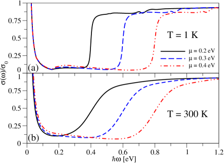
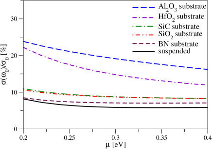
Figure 2 shows the optical conductivity for graphene on a SiO2 substrate at different temperatures and chemical potentials. Apart from the trends in the behavior of the optical conductivity discussed above, one can clearly see different gaps in the absorption spectrum, given by for each chemical potential. Another feature that can be discerned from Fig. 2 is that the maximal value of the phonon-mediated absorption in the gap increases with increasing chemical potential (doping level). Moreover, we note that due to the electron-hole symmetry of the Dirac Hamiltonian, the profiles of the optical conductivity would look the same for -doped graphene. The dependence of the midgap absorption on the chemical potential at room temperature is shown in Fig. 3, again for suspended graphene and graphene on several different substrates. In the region studied here between eV and eV, the midgap absorption decreases with increasing chemical potential for graphene on substrates, with the decay being most pronounced for HfO2. The differences in the shape of the phonon mediated gap absorption reflect the momentum dependence of the electron-phonon interaction in Eq. (5)-(7).
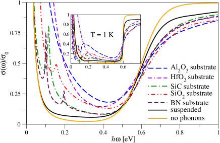
In particular, Fig. 4 reveals a striking difference in the absorption if we use a bare unscreened Fröhlich couplings. If screening is not accounted for, we find that the optical conductivity in the optical gap is greatly enhanced compared to the situation where screening is used. The most noticeable feature if the bare Fröhlich coupling is used, is that a second clearly distinguishable phonon sideband peak (due to the SPPs) can now be observed in the absorption spectra even at room temperature for SiO2 and SiC substrates. For BN substrates, one can even find two such peaks at room temperature. We suggest, therefore, that measurements of the midgap absorption in graphene on different substrates could help to clarify the still controversialKonar et al. (2010); Li et al. (2010); Price et al. (2012); Fischetti et al. (2001); Ong and Fischetti (2012) issue concerning the effect of screening on the electron-SPP coupling strength.
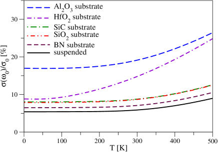
We also investigate the temperature dependence of the midgap conductivity (that is, at ) within our model in Fig. 5 on several different substrates. At temperatures below 100 K, the midgap absorption does not depend strongly on the temperature. At about 100 K, an increase of the optical conductivity at is predicted to take place. Also, the smaller the energy of the dominant phonon contributing to the gap absorption, the stronger is the temperature dependence in Fig. 5.
Finally, we relate the midgap absorption to the spectral weight of the Drude peak. Describing the graphene optical conductivity in the non-interacting single-particle picture, the spectral weight of the bare Drude peak is , where is the bare Drude weight and is some characteristic frequency much larger than the scattering rate, but smaller than both the lowest energy of the optical phonon and . In the presence of phonons, the total spectral weight has to be conserved. The spectral weight contribution due to the midgap absorption can be approximated at low temperatures as , where is the averaged value of , that is, of the real part of the optical conductivity, in units of . If we further assume that the entire spectral weight lost at the Drude peak is transferred to the optical gap and that , within this picture the remaining Drude weight can then be estimated as . Thus, from this consideration we expect that, as increases with increasing temperature or strength of the electron-phonon coupling, the Drude weight is reduced.
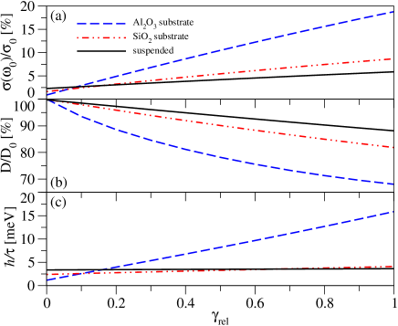
Figure 6 shows (a) the absorption in the optical gap as well as the fitted (b) Drude weight and (c) inverse scattering time for suspended graphene and graphene on Al2O3 and SiO2 substrates with eV, K, and cm-2 as functions of the relative strength of the electron-phonon coupling. Here, the optical conductivities have been calculated by scaling the (products of) electron-phonon coupling matrix elements with , and the Drude weight as well as the inverse scattering time have been extracted from the optical conductivity by fitting the Drude peak to a Lorentzian. As expected from the argument given above, the Drude weight decreases with increasing , although the simple relationship between reduced Drude weight loss and the midgap absorption as does not hold. This is because the midgap absorption does not coincide with the averaged value of in the gap and because some of the spectral weight from the Drude peak is transferred not only to the optical gap, but also to the spectral region .
With increasing , electron-phonon scattering becomes more probable and consequently the scattering time decreases as can be seen in Fig. 6 (c). The corresponding increase of is most pronounced for graphene on Al2O3 and least pronounced for suspended graphene. Finally, we remind the reader that for cm-2 impurity scattering also contributes to the absorption in the optical gap, which can be discerned from the finite absorption at . Because suspended graphene and graphene on different substrates each possess different background dielectric constants and thus different transport scattering times, the residual values at are also different.
IV Conclusions
We have studied the effects of intrinsic graphene optical phonons and SPPs on the optical conductivity of doped graphene. Our focus has been on the absorption at frequencies , where optical transitions are forbidden due to Pauli blocking in a clean system (at ), but which can occur if phonons are present, giving rise to phonon sidebands. Here, we have found that inelastic phonon scattering contributes significantly to the absorption in the optical gap and strongly depends on the substrate used: At room temperature (and eV), the midgap absorption, which is mainly due to intrinsic optical phonons, amounts to about 5-6% of the universal ac conductivity for suspended graphene or graphene on non-polar substrates, while the midgap absorption can be as large as 20-25% of for graphene on polar substrates (such as Al2O3 or HfO2) due to the smaller SPP energy and strong electron-SPP coupling. Moreover, the midgap absorption depends on the doping level and decreases with increasing , while the maximal value of the sideband absorption at low temperatures increases. We have also investigated the temperature dependence of the midgap absorption which increases with increasing temperature. The Drude peak, on the other hand, becomes broader with increasing temperature as inelastic electron-phonon scattering becomes more important. Consequently, the Drude weight decreases with increasing temperature due to the stronger phonon coupling.
Acknowledgements.
We gratefully acknowledge Fengnian Xia from IBM for stimulating discussions and Alex Matos-Abiague and Christian Ertler from the University of Regensburg for technical discussions. B.S. and J.F. acknowledge support from DFG Grants No. SFB 689 and No. GRK 1570.Appendix A Self-energy and Green’s Function
We use standard diagrammatic perturbation theory (with the unperturbed Hamiltonian and the perturbation ) to calculate the electronic Matsubara Green’s function of the system described by Eq. (4),
| (16) |
where and denote the imaginary time and (fermionic) frequency, the thermal average, the imaginary time-ordering operator, and .Mahan (2000); Fetter and Walecka (2003); Bruus and Flensberg (2006) By solving the corresponding Dyson equation, we can express the electronic Green’s function via the self-energy . In writing down Eq. (16), we have used that, due to the conservation of momentum and spin, the self-energy and thus the Green’s function are diagonal in and and do not depend on due to spin degeneracy.
Up to the first non-vanishing order (and omitting the tadpole diagram, which yields a purely real self-energy contribution that can be absorbed in the chemical potential), we find the electronic self-energy due to phonons for arbitrary matrix elements to beMahan (2000)
| (17) | ||||
with the Fermi-Dirac and Bose-Einstein distribution functions, and , and the chemical potential at the temperature . Thus, in the lowest order, the self-energy is simply the sum of the contributions from the different phonons .
In order to calculate the self-energy, we need to know the products of the electron-phonon coupling matrix elements entering Eq. (17), , for the , , SO1, and SO2 modes. Since , it follows from Eqs. (17) and (5) that the contribution due to the optical phonons near the point is diagonal in the valley and band quantum numbers. We calculate the self-energy by using the transformation and replacing the sum by the 2D integral , where and is chosen to be the angle between and .
Equation (6) describes the coupling of the mode to the electrons in graphene. As above, the self-energy contribution from the phonons is calculated by introducing and writing the sum as a 2D integral. After performing the integration over the angle , the terms containing in Eq. (6) vanish and consequently the contribution to the self-energy is diagonal with respect to the band quantum number. Moreover, Eqs. (6) and (17) make it clear that, even though the matrix element describes intervalley scattering, the second-order contribution from the phonon to the self-energy is diagonal also in the valley quantum number.
Using the SPP coupling matrix elements (7), the contribution from each SPP to the self-energy is again calculated by introducing and writing the sum as a 2D integral. Then, the angular integration for the offdiagonal elements with respect to the band indices and is of the type , where the function depends only on and on the SPP considered, and vanishes for screened as well as unscreened SPPs. Thus, the lowest order contribution from each SPP to the self-energy is also diagonal in the band and valley quantum numbers.
Combining the results discussed so far, the total contribution from all phonons is given by
| (18) |
where is given by
| (19) | ||||
and each individual contribution is calculated from Eq. (17) as described above for and . Here, we find that, in contrast to the contributions and , the contributions from the graphene optical phonons, and , do not depend on the band or momentum .
The contribution due to Coulomb impurity scattering reads as
| (20) |
where
| (21) | ||||
with , , the dielectric function , and the impurity concentration .Hwang and Das Sarma (2009) Since this contribution is also diagonal, the total self-energy
| (22) | ||||
and, consequently, the Green’s function
| (23) | ||||
are diagonal with respect to and in our model. Finally, the spectral function is obtained from the Green’s function via
| (24) |
In this work, we are interested only in the imaginary parts of the retarded self-energy. Upon replacing by in Eq. (17), the imaginary part of each contribution in Eq. (17) contains a Dirac- function [since there is no contribution from as discussed above]. After introducing and writing the sum as a 2D integral, the Dirac- function can be used to calculate the integral, which then yields Eq. (12) for the and phonons and Eqs. (13) and (14) for the SO1 and SO2 phonons.
Appendix B Kubo formula for the optical conductivity
B.1 Current density operator
Our starting point in the derivation of a Kubo formula for the optical conductivity is the current operator. In the presence of an arbitrary magnetic vector potential , the (first-quantized) 2D Dirac Hamiltonian of graphene reads asCastro Neto et al. (2009)
| (25) |
with being the 2D kinetic momentum operator, the 2D momentum operator, and the matrices , , , where is the unity matrix and and are Pauli matrices referring to the sublattices and the points, respectively. As discussed in Ref. Castro Neto et al., 2009, the 2D momentum and the valley are good quantum numbers and the Hamiltonian (25) has the (valley-degenerate) eigenvalues
| (26) |
and the corresponding eigenstates
| (27) |
near the point and
| (28) |
near the point, where denotes the surface area of the graphene sample, , , and
| (29) |
For an arbitrary (normalized) state , the energy expectation value as a functional of the vector potential is given by
| (30) |
where the sums over and refer to the matrix . The charge current density of this state can be determined by a variational method:
| (31) |
which yields
| (32) |
Promoting the wave functions in Eq. (32) to field operators, using the eigenbasis given by Eqs. (26)-(28), and taking into account the spin degeneracy, the charge current density operator can be determined as
| (33) |
in reciprocal space and as
| (34) |
in real space. Here, the dipole matrix elements read as
| (35) | |||
B.2 Kubo formula
If an external electric field
| (36) |
is applied to the system considered here, its effect can be described by
| (37) |
with the charge current density operator (34). The total Hamiltonian of the problem then reads as , where is given by Eq. (4).
Using linear response theory [for the unperturbed Hamiltonian and the perturbation ] and conducting a Fourier transformation with respect to the time and position,Mahan (2000); Fetter and Walecka (2003); Bruus and Flensberg (2006) we find that the current density due to the external field is given by
| (38) |
with being the (Fourier transformed) retarded current-current correlation function and and referring to the in-plane coordinates and . The retarded correlation function can be related to the imaginary-time correlation function
| (39) |
by , that is, by replacing with in Eq. (39).Mahan (2000); Fetter and Walecka (2003); Bruus and Flensberg (2006) Here, denotes a bosonic frequency. Hence, the Kubo formula for the real part of the conductivity reads as
| (40) |
References
- Novoselov et al. (2004) K. S. Novoselov, A. K. Geim, S. V. Morozov, D. Jiang, Y. Zhang, S. V. Dubonos, I. V. Grigorieva, and A. A. Firsov, Science 306, 666 (2004).
- Novoselov et al. (2005) K. S. Novoselov, A. K. Geim, S. V. Morozov, D. Jiang, M. I. Katsnelson, I. V. Grigorieva, S. V. Dubonos, and A. A. Firsov, Nature (London) 438, 197 (2005).
- Geim and Novoselov (2007) A. K. Geim and K. S. Novoselov, Nat. Mater. 6, 183 (2007).
- Castro Neto et al. (2009) A. H. Castro Neto, F. Guinea, N. M. R. Peres, K. S. Novoselov, and A. K. Geim, Rev. Mod. Phys. 81, 109 (2009).
- Zhang et al. (2005) Y. Zhang, Y.-W. Tan, H. L. Stormer, and P. Kim, Nature (London) 438, 201 (2005).
- Bolotin et al. (2008) K. Bolotin, K. Sikes, Z. Jiang, M. Klima, G. Fudenberg, J. Hone, P. Kim, and H. Stormer, Solid State Commun. 146, 351 (2008).
- Du et al. (2008) X. Du, I. Skachko, A. Barker, and E. Y. Andrei, Nature Nanotech. 3, 491 (2008).
- Peres (2010) N. M. R. Peres, Rev. Mod. Phys. 82, 2673 (2010).
- Das Sarma et al. (2011) S. Das Sarma, S. Adam, E. H. Hwang, and E. Rossi, Rev. Mod. Phys. 83, 407 (2011).
- Geim (2009) A. K. Geim, Science 324, 1530 (2009).
- Avouris (2010) P. Avouris, Nano Letters 10, 4285 (2010).
- Bonaccorso et al. (2010) F. Bonaccorso, Z. Sun, T. Hasan, and A. C. Ferrari, Nature Phot. 4, 611 (2010).
- Nair et al. (2008) R. R. Nair, P. Blake, A. N. Grigorenko, K. S. Novoselov, T. J. Booth, T. Stauber, N. M. R. Peres, and A. K. Geim, Science 320, 1308 (2008).
- Li et al. (2008) Z. Q. Li, E. A. Henriksen, Z. Jiang, Z. Hao, M. C. Martin, P. Kim, H. L. Stormer, and D. N. Basov, Nat. Phys. 4, 532 (2008).
- Mak et al. (2008) K. F. Mak, M. Y. Sfeir, Y. Wu, C. H. Lui, J. A. Misewich, and T. F. Heinz, Phys. Rev. Lett. 101, 196405 (2008).
- Horng et al. (2011) J. Horng, C.-F. Chen, B. Geng, C. Girit, Y. Zhang, Z. Hao, H. A. Bechtel, M. Martin, A. Zettl, M. F. Crommie, et al., Phys. Rev. B 83, 165113 (2011).
- Peres et al. (2006) N. M. R. Peres, F. Guinea, and A. H. Castro Neto, Phys. Rev. B 73, 125411 (2006).
- Gusynin and Sharapov (2006) V. P. Gusynin and S. G. Sharapov, Phys. Rev. B 73, 245411 (2006).
- Falkovsky and Pershoguba (2007) L. A. Falkovsky and S. S. Pershoguba, Phys. Rev. B 76, 153410 (2007).
- Stauber et al. (2008a) T. Stauber, N. M. R. Peres, and A. H. Castro Neto, Phys. Rev. B 78, 085418 (2008a).
- Stauber et al. (2008b) T. Stauber, N. M. R. Peres, and A. K. Geim, Phys. Rev. B 78, 085432 (2008b).
- Carbotte et al. (2010) J. P. Carbotte, E. J. Nicol, and S. G. Sharapov, Phys. Rev. B 81, 045419 (2010).
- Peres et al. (2010) N. M. R. Peres, R. M. Ribeiro, and A. H. Castro Neto, Phys. Rev. Lett. 105, 055501 (2010).
- Abedinpour et al. (2011) S. H. Abedinpour, G. Vignale, A. Principi, M. Polini, W.-K. Tse, and A. H. MacDonald, Phys. Rev. B 84, 045429 (2011).
- Vasko et al. (2012) F. T. Vasko, V. V. Mitin, V. Ryzhii, and T. Otsuji, Phys. Rev. B 86, 235424 (2012).
- Liu et al. (2011) M. Liu, X. Yin, E. Ulin-Avila, B. Geng, T. Zentgraf, L. Ju, F. Wang, and X. Zhang, Nature 474, 64 (2011).
- Liu et al. (2012) M. Liu, X. Yin, and X. Zhang, Nano Lett. 12, 1482 (2012).
- Bao and Loh (2012) Q. Bao and K. P. Loh, ACS Nano 6, 3677 (2012).
- de Juan et al. (2010) F. de Juan, E. H. Hwang, and M. A. H. Vozmediano, Phys. Rev. B 82, 245418 (2010).
- Min et al. (2011) H. Min, D. S. L. Abergel, E. H. Hwang, and S. Das Sarma, Phys. Rev. B 84, 041406 (2011).
- Abergel et al. (2012) D. S. L. Abergel, H. Min, E. H. Hwang, and S. Das Sarma, Phys. Rev. B 85, 045411 (2012).
- Gusynin et al. (2007) V. P. Gusynin, S. G. Sharapov, and J. P. Carbotte, Phys. Rev. Lett. 98, 157402 (2007).
- Pound et al. (2012) A. Pound, J. P. Carbotte, and E. J. Nicol, Phys. Rev. B 85, 125422 (2012).
- Price et al. (2012) A. S. Price, S. M. Hornett, A. V. Shytov, E. Hendry, and D. W. Horsell, Phys. Rev. B 85, 161411 (2012).
- Low et al. (2012) T. Low, V. Perebeinos, R. Kim, M. Freitag, and P. Avouris, Phys. Rev. B 86, 045413 (2012).
- Petrov and Rotkin (2013) A. G. Petrov and S. V. Rotkin, to be published (2013).
- Meric et al. (2008) I. Meric, M. Y. Han, A. F. Young, B. Ozyilmaz, P. Kim, and K. L. Shepard, Nature Nanotech. 3, 654 (2008).
- Perebeinos et al. (2009) V. Perebeinos, S. V. Rotkin, A. G. Petrov, and P. Avouris, Nano Lett. 9, 312 (2009).
- Chandra et al. (2011) B. Chandra, V. Perebeinos, S. Berciaud, J. Katoch, M. Ishigami, P. Kim, T. F. Heinz, and J. Hone, Phys. Rev. Lett. 107, 146601 (2011).
- Barreiro et al. (2009) A. Barreiro, M. Lazzeri, J. Moser, F. Mauri, and A. Bachtold, Phys. Rev. Lett. 103, 076601 (2009).
- Freitag et al. (2009) M. Freitag, M. Steiner, Y. Martin, V. Perebeinos, Z. Chen, J. C. Tsang, and P. Avouris, Nano Lett. 9, 1883 (2009).
- Perebeinos and Avouris (2010) V. Perebeinos and P. Avouris, Phys. Rev. B 81, 195442 (2010).
- Konar et al. (2010) A. Konar, T. Fang, and D. Jena, Phys. Rev. B 82, 115452 (2010).
- Li et al. (2010) X. Li, E. A. Barry, J. M. Zavada, M. B. Nardelli, and K. W. Kim, Appl. Phys. Lett. 97, 232105 (2010).
- DaSilva et al. (2010) A. M. DaSilva, K. Zou, J. K. Jain, and J. Zhu, Phys. Rev. Lett. 104, 236601 (2010).
- Chen et al. (2008) J. H. Chen, C. Jang, S. Xiao, M. Ishigami, and M. S. Fuhrer, Nature Nano. 3, 206 (2008).
- Fratini and Guinea (2008) S. Fratini and F. Guinea, Phys. Rev. B 77, 195415 (2008).
- Farmer et al. (2011) D. B. Farmer, V. Perebeinos, Y.-M. Lin, C. Dimitrakopoulos, and P. Avouris, Phys. Rev. B 84, 205417 (2011).
- Chiu et al. (2010) H.-Y. Chiu, V. Perebeinos, Y.-M. Lin, and P. Avouris, Nano Lett. 10, 4634 (2010).
- Mahan (2000) G. D. Mahan, Many-Particle Physics (Kluwer/Plenum, New York, 2000).
- Piscanec et al. (2004) S. Piscanec, M. Lazzeri, F. Mauri, A. C. Ferrari, and J. Robertson, Phys. Rev. Lett. 93, 185503 (2004).
- Lazzeri et al. (2005) M. Lazzeri, S. Piscanec, F. Mauri, A. C. Ferrari, and J. Robertson, Phys. Rev. Lett. 95, 236802 (2005).
- Perebeinos et al. (2005) V. Perebeinos, J. Tersoff, and P. Avouris, Phys. Rev. Lett. 94, 086802 (2005).
- Ando (2006) T. Ando, J. Phys. Soc. Jpn. 75, 124701 (2006).
- Lazzeri et al. (2008) M. Lazzeri, C. Attaccalite, L. Wirtz, and F. Mauri, Phys. Rev. B 78, 081406 (2008).
- Borysenko et al. (2010) K. M. Borysenko, J. T. Mullen, E. A. Barry, S. Paul, Y. G. Semenov, J. M. Zavada, M. B. Nardelli, and K. W. Kim, Phys. Rev. B 81, 121412 (2010).
- Wang and Mahan (1972) S. Q. Wang and G. D. Mahan, Phys. Rev. B 6, 4517 (1972).
- Fischetti et al. (2001) M. V. Fischetti, D. A. Neumayer, and E. A. Cartier, J. Appl. Phys. 90, 4587 (2001).
- Wunsch et al. (2006) B. Wunsch, T. Stauber, F. Sols, and F. Guinea, New J. Phys. 8, 318 (2006).
- Hwang and Das Sarma (2007) E. H. Hwang and S. Das Sarma, Phys. Rev. B 75, 205418 (2007).
- Ong and Fischetti (2012) Z.-Y. Ong and M. V. Fischetti, Phys. Rev. B 86, 165422 (2012).
- Geick et al. (1966) R. Geick, C. H. Perry, and G. Rupprecht, Phys. Rev. 146, 543 (1966).
- Harris (1995) G. Harris, Properties of Silicon Carbide (INSPEC, Institution of Electrical Engineers, London, UK, 1995).
- Fetter and Walecka (2003) A. L. Fetter and J. D. Walecka, Quantum Theory of Many-Particle Systems (Dover Publ., Mineola, N.Y., 2003).
- Bruus and Flensberg (2006) H. Bruus and K. Flensberg, Many Body Quantum Theory in Condensed Matter Physics (Oxford Univ. Press, Oxford, 2006).
- Hwang and Das Sarma (2009) E. H. Hwang and S. Das Sarma, Phys. Rev. B 79, 165404 (2009).