Unconventional spin texture of a topologically nontrivial semimetal Sb(110)
Abstract
The surfaces of antimony are characterized by the presence of spin-split states within the projected bulk band gap and the Fermi contour is thus expected to exhibit a spin texture. Using spin-resolved density functional theory calculations, we determine the spin polarization of the surface bands of Sb(110). The existence of the unconventional spin texture is corroborated by the investigations of the electron scattering on this surface. The charge interference patterns formed around single scattering impurities, imaged by scanning tunneling microscopy, reveal the absence of direct backscattering signal. We identify the allowed scattering vectors and analyze their bias evolution in relation to the surface-state dispersion.
Pure bismuth and antimony are group-V semimetals and their surfaces support spin-orbit split surface states existing within the projected bulk band gap [1]- [5]. The two materials differ however, with respect to the topological character of their bulk bands. Whereas pure bismuth is topologically trivial, adding a small amount of Sb into Bi is enough to drive the system into a topological insulator phase [6, 7]. The spin-nondegenerate surface states of the topological insulator Bi(1-x)Sbx (0.09x0.18) continuously connect the valence and the conduction band and their existence is derived directly from the fundamental considerations of the parity characteristics of the bulk bands [8]. As more Sb is added into the alloy, the system becomes semimetallic again, it keeps however the nontrivial topological order of the bulk bands [7]. Thus, the other extreme case of the Bi(1-x)Sbx alloy, pure antimony, is a semimetal with bulk characteristic of a strong topological insulator.
The (111) surfaces of the topologically nontrivial materials, including the Bi(1-x)Sbx alloy and Sb, have been extensively investigated by spin and angle resolved photoemission spectroscopy (ARPES) and scanning tunneling microscopy (STM) [4]-[7],[9]-[12]. These studies allowed to determine the spin textures [5, 9, 10], map the surface band dispersion [4]-[7] and revealed an unconventional electron dynamics [11, 12, 13]. At the same time, studies addressing non-(111) surfaces of those materials are almost nonexistent. Only recently, we have shown that Sb(110) exhibits spin-split surface states but, contrary to predictions based on its bulk topology, their dispersion properties are those of a trivial material . This is due to the semimetallic character of the surface, which relaxes the character of the surface state bands imposed by the bulk topology [3]. The spin polarization of these surface bands remains, however, still unknown. Since Antimony has a weaker spin-orbit coupling than bismuth, it is crucial to prove if a sufficient degree of spin polarization still remains in the split surface bands and how it affects its electron scattering properties.
The spin texture of the surface bands can be addressed indirectly by investigating the electron scattering processes [12],[14]-[17]. The spin-orbit coupling affects the electron scattering probabilities, making them dependent on the overlap of the spin wavefunctions of the final and initial scattering state. In particular, the characteristic feature of spin-orbit coupled systems is the suppression of direct backscattering, because the states with opposite momenta are required to have orthogonal spins by time reversal symmetry [14, 18]. The modulation in the charge local density of states (LDOS) which arises due to the interference of the electrons scattering at surface impurities is directly accessible with scanning tunneling microscopy and spectroscopy (STS). The scattering vectors , connecting the initial and final states in the reciprocal space, can be identified by examining the Fourier transform (FT) of the interference patterns [19]. By demonstrating the lack of backscattering signal, this method allowed to confirm the existence of the spin texture at the surfaces of semimetallic bismuth and antimony [13, 14, 17] as well as topological insulators Bi(1-x)Sbx , Bi2Se3 and Bi2Te3 [12, 15, 16].
In this paper, we investigate the electron scattering processes on a non-(111) surface of topologically nontrivial material, Sb(110), in order to gain experimental insight into the spin texture of its surface electronic bands. We observe strong modulation in the LDOS around single adatoms on the surface and correlate the features in the Fourier transformed images to the specific scattering vectors. We identify those scattering events by analyzing the Fermi contour measured by ARPES and the spin polarization of the surface bands predicted by relativistic density functional theory (DFT) calculations. The resulting spin texture is highly anisotropic and strongly varies with the character of the bands, deviating from the conventional picture of a Rashba surface. The experimental STM data do not show any direct backscattering between the nondegenerate surface bands, confirming their spin-split nature and the spin texture of the Fermi contour.
We have investigated the surface electronic structure of Sb(110) using STM and ARPES. The STM exeriments were performed in a custom-made microscope working in an ultrahigh vacuum at 5 K. The ARPES data were taken at the SGM-III beamline of the synchrotron radiation facility ASTRID in Aarhus [20]. The combined energy and angular resolution were better than 10 meV and , respectively. The data shown here were all taken using a photon energy of 20 eV. During the photoemission measurements the sample was kept at a temperature of 60 K. The Sb(110) single crystal surface was cleaned by repeated sputtering and annealing cycles.
We modeled the electronic and spin structure of the Sb(110) using a non-collinear DFT [21, 22] within the Perdew-Burke-Ernzerhof implementation [23] of the generalized gradient approximation. We considered a repeated slab system consisting of 54 layers relaxed up to forces Ry/a.u. and used fully relativistic norm-conserving pseudopotentials as described in Ref. [21] with the energy cutoff corresponding to Ec=60 Ry. In order to calculate the projection of the bulk band structure onto the (110) surface, we have also used the tight-binding scheme of Liu and Allen [24].
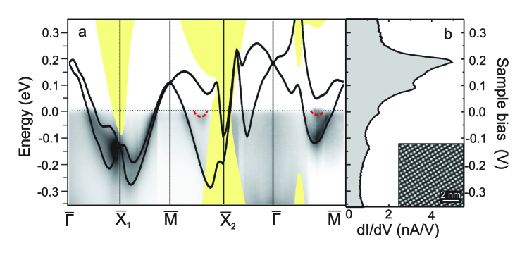
The Sb(110) surface shows several spin-orbit split surface states within the projected bulk band gap. In Figs. 1 and 2 we present electronic structure of Sb(110) as measured by ARPES and calculated by DFT. The dispersion of the surface bands and their topological character were discussed in detail in Ref. [3]. Here, we summarize the most important properties of this surface, which directly affect the electron scattering processes, i.e. the dispersion of the surface bands in the vicinity the Fermi level and their spin texture. The electronic structure of Sb(110) along certain high symmetry directions is shown in Fig. 1(a) and the experimentally determined Fermi contour is presented in Fig. 2(c) (grey-scale background). For clarity, the lines have been superimposed on the data in Fig. 2(c), showing schematically the shape of the contour. The most important spectroscopic features which we identify in both calculations and the experimental data are: (i) the hole pocket around the point, giving rise to circular contour in Fig. 2(c), (ii) a pocket around , identified in the Fermi contour as a ’butterfly’ shaped feature; (iii) an extended hole pocket around , observed as a weak feature in ARPES data. In addition, ARPES reveals a very shallow electron pocket (dotted lines in Fig. 1(a) in and directions), which is not well reproduced by the calculations. This pocket is particularly important to understand the electron scattering dynamics in the vicinity of the Fermi level, since it contributes strongly to the density of states in this energy window [14]. In fact, the experimentally measured dI/dV spectrum (Fig. 1(b)), which reflects the LDOS of a clean Sb(110) surface, shows a peak in the vicinity of the Fermi level, marking the onset of the electron pocket. Several other sharp features in the dI/dV spectrum correspond to the onset (negative bias) and the top (positive bias) of the surface bands. Due to the relatively weak spin-orbit coupling in Sb, the splitting of the bands is rather small so that in certain parts of the Brillouin zone the two spin partners are close to being degenerate. Accordingly, some of the features of the Fermi contour in Fig. 2(c), the high intensity feature along direction and crossing along direction, are double crossings and the two states with opposite spin become almost degenerate.
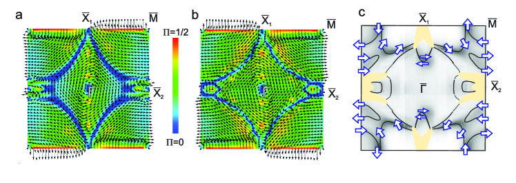
To determine the spin of the Fermi contour we calculated the spin texture of the upper and lower subband within the first Brillouin zone, as shown in Fig, 2(a) and (b), respectively. The degree of certainty about the electron spin, , is represented by the color scale in the background ( ). The direction of the spin in the surface plane is depicted by arrows. The polarization out of plane becomes important only for the lower subband, close to the point. Across the rest of the Brillouin zone, the expectation value of the polarization out of plane remains very small. The spin texture of any constant energy contour can be now defined by considering separately the spin polarization for the lower and upper subband. In Fig. 2(c) the spin polarization deduced from plots in (a) and (b) is superimposed on the Fermi contour of Sb(110). We find that the spin direction is almost constant as we move along one side of the butterfly-shaped pocket and rotates along the pockets. The features along and correspond to almost double crossings and, consequently, have contributions from both spin-split bands, and thus, two opposite spins.
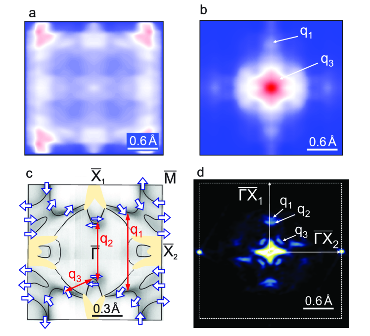
The spin texture of the constant energy contours will affect the scattering of the electrons by the surface impurities. In particular, the systems with spin-orbit split surface states are characterized by the absence of direct backscattering, imposed by the time reversal symmetry [18]. In order to experimentally verify the spin texture of Sb(110) and identify the allowed scattering vectors we analyzed the charge interference patterns formed by electrons scattering on a single adatom (Fig. 3). In the bias range between -80 and 240 meV we observe pronounced modulation in the LDOS signal. A series of dI/dV spectroscopic images in Fig. 3(b)-(g) shows the evolution of the patterns for several chosen bias voltages. The Fast Fourier Transform (FFT) of the images ((i)-(n)) shows high intensity features, corresponding to the allowed scattering vectors .
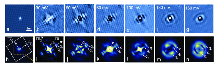
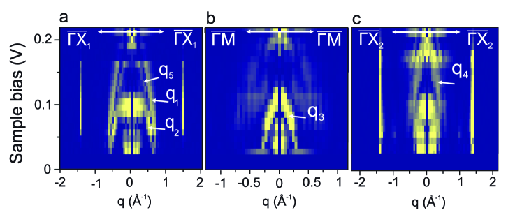
Close to the Fermi level ((i) and (j)) the most distinctive features of the FFT [25] are two double arc-shaped features along direction (labeled and ) and the four spots lying symmetrically around the center (labelled ). The features disperse with increasing sample bias as shown in more detail in Fig. 4(a)-(c). Each graph represents a set of the linescans through the FFT images taken at different sample bias in certain high symmetry direction (, and , respectively). The vectors and get smaller until at around 100 meV the feature vanishes from the FFT and the transform into a cicular shape. The four features move to the center of the FFT and disappear also around at 100 meV. At the same bias range two more scattering events appear: the features in the direction and in the direction .
In order to establish the origin of the features observed in FFT, we consider the shape and spin texture of the constant energy contour. In the simple picture, the scattering probability at energy , between the -states separated by the scattering vector , is determined by the electron density of states of the final and the initial state, weighted by the overlap of the spinor wavefunctions [12]:
| (1) |
Thus, the spin dependent part of the scattering amplitude will be maximal if the initial and final spins are parallel and zero when the two spins are antipararell.
If the spin contribution to the scattering amplitudes is neglected, the map of the scattering vectors allowed by the Fermi contour can be evaluated directly from the photoemission data, by calculating the convolution of the ARPES spectra. The autocorrelation image (AC-ARPES) can be derived from the ARPES intensities , as [26, 27]:
| (2) |
The AC-ARPES defined in this way reproduces the features of the joint density of states (JDOS), which in turn maps out the LDOS contribution to the scattering probabilities. While the quantitative comparison between AC-ARPES and JDOS is not straightforward, since the ARPES intensities are related to the electron spectral function through an energy and -dependent matrix element, the autocorrelation image stills allows for a qualitative analysis of the scattering vectors [26, 27]. For spin degenerate Fermi contour, the AC-ARPES can be directly compared to the FFT of the interference patterns resolved by STM at low bias [27].
We have calculated the AC-ARPES map for Sb(110) (Fig. 5(a)), neglecting its spin texture, and compared it to the FT-STM map measured close to the Fermi level (Fig. 5(d)). We find that certain parts of the AC-ARPES are suppressed in the STM data. In fact, many of the features present in AC-ARPES but absent in the FFT map can be identified as direct backscattering events, which are expected to be prohibited by the spin texture of Sb(110). Thus, to describe the experimental STM data more accurately, we introduce into the cross-correlation integral (Eq. (2)) an additional term: . While this basic term does not account for the anisotropic spin texture of Sb(110), it suppresses the backscattering in a simple way. The result (Fig. 5(b)) reproduces the FFT map to a greater degree. Large parts of the original AC-ARPES map in Fig. 5(b) are now diminished and the remaining features correspond relatively well to the main spots of the FFT. We can thus conclude that the backscattering is indeed absent on Sb(110) surface, confirming the spin-split character of its surface bands.
We can now associate the spots resolved in the FT-STM map (Fig. 5(d)) with the specific scattering vectors. First, we identify the feature as interband scattering between the edges of the ’butterfly wings’ in direction (Fig. 5(c)). This feature of the Fermi contour corresponds to a very shallow and extended electron pocket and is thus expected to have a high DOS and contribute strongly to the scattering at this energy range. With increasing bias, disperses very steeply (see Fig. 4(a)), reflecting the dispersion of the left band which forms the electron pocket in direction. In principle, the scattering between the ’butterfly wings’ should also give rise to features in FFT in the direction. They are indeed resolved in the AC-ARPES images Fig. 5(a) but we observe them only as faint spots in FT-STM image, possibly due to partial suppression by the overlap of the spinor wavefunctions. Next, we assign the feature to the backscattering between the -crossing points. At first glance, such scattering event seems to violate the time-reversal symmetry. However, at this point of the Fermi contour the two spin-split bands are close to be degenerate. Therefore both spin partners are present, allowing the backscattering process, in a similar way as it happens on a Au(111) surface [18]. Since backscattering is a preferred scattering process on metal surfaces, this feature has a rather high intensity in the FFT [18]. The AC-ARPES map in Fig. 4(b) does not reproduce it though, as the term included in the integral excludes all the backscattering processes. This assignment of is further confirmed by the bias evolution of this feature (Fig. 4(a)). As the energy increases, the bands which cross the Fermi level along direction disperse towards the point. Thus, the feature moves towards the center of the FT-STM image (Fig. 4(a)), until the top of the band is reached and it disappears from the FFT. This point at is not accurately reproduced by the band structure calculations in Fig. 1a (), what we attribute to the inability of DFT to reproduce all fine structure details in the meV range. The spots marked as result from the forward scattering between the edges of the butterfly wing (the electron pocket) and the -crossing point. The analysis of the band’s dispersion also shows that these features should move toward the center of the FFT image (Fig. 4(c)).
The identification of the scattering events far above the Fermi level ( and ) is not as clear, because of the uncertainties in the calculated dispersion and the absence of photoemission data. We can tentatively explain their origin by the appearance of the new high DOS feature (peak at 100 meV in Fig. 1(b)), when the sample bias reaches the top of the bands near the and point.
It is interesting to compare these results to the previous study of electron scattering on Bi(110), another extreme case of the BiSb alloy. In Bi(110) the pronounced spin-splitting of the surface bands leads to a clear manifestation of the spin-dependent scattering process. In fact, only spin conserving scattering events are observed in the Fourier transformed dI/dV maps on Bi(110) [14, 17].
Antimony has a smaller spin-orbit coupling and the spin-split of the bands is generally smaller [3]. Although, the bands maintain a certain spin texture (as evidenced in Fig. 2), the role of the spin in the formation of the interference patterns is experimentally less evident, and certain backscattering events could be identified. These are caused because at certain points of the Fermi surface with high DOS, the two sub-bands are so close in K-space that scattering between them will resemble the backscattering events in the interference patterns, in a similar way as described in Ref. [18].
In summary, we have predicted theoretically and confirmed experimentally the unconventional spin texture of the Sb(110) surface. In spite of a smaller spin-orbit coupling, the spin polarization of the surface bands still dominates the electron dynamics of this surface. The LDOS interference patterns formed around single impurities reveal the dominance of non-direct backscattering events as in the related compound Bi(110). The identification of the scattering events was done combining ARPES measurements at EF with the state’s dispersion above EF, measured from energy dependent differential conductance maps, and interpreted on the basis of DFT calculations of the spin texture and dispersion of the surface state bands. The smaller spin-orbit interaction of Sb(110) is reflected in a smaller band splitting what, in some cases, give rise to interband scattering with wavevectors close to the pure backscattering case.
References
References
- [1] Agergaard A, Søndergaard Ch, Li H, Nielsen M B, Hoffmann S V, Li Z and Hofmann Ph 2001 New J. Phys. 3 15
- [2] Hofmann Ph 2006 Prog. Surf. Sci. 81 191
- [3] Bianchi M, Guan D, Strozecka A, Voetmann C H, Bao S, Pascual J I, Eiguren A and Hofmann Ph 2012 Phys. Rev. B 85 155431
- [4] Sugawara K, Sato T, Souma S, Takahashi T, Arai M and T Sasaki 2006 Phys. Rev. Lett. 96 046411
- [5] Kadono T, Miyamoto K, Nishimura R, Kanomaru K, Qiao S, Shimada K, Namatame H, Kimura A and Taniguchi M 2008 Appl. Phys. Lett. 93 252107
- [6] Hsieh D, Qian D , Wray L, Xia Y, Hor Y S, Cava R J and Hasan M Z 2008 Nature 452 970
- [7] Guo H, Sugawara K, Takayama A, Souma S, Sato T, Satoh N, Ohnishi A, Kitaura M, Sasaki M, Xue Q K and Takahashi T 2011 Phys. Rev. B 83 201104
- [8] Teo J C Y, Liang Fu and Kane C L 2008 Phys. Rev. B 78 045426
- [9] Hsieh D, Xia Y, Wray L, Qian D, Pal A, Dil J H, Osterwalder J, Meier F, Bihlmayer G, Kane C L, Hor Y S, Cava R J and Hasan M Z 2009 Science 323 919
- [10] Hsieh D, Wray L, Qian D, Xia Y, Dil J H, Meier F, Patthey L, Osterwalder J, Bihlmayer G, Hor Y S, Cava R J and Hasan M Z 2010 New J. Phys. 12 125001
- [11] Park S R, Jung W S, Han G R, Kim Y K, Kim Chul, Song D J, Koh Y Y, Kimura S, Lee K D, Hur N, Kim J Y, Cho B K, Kim J H, Kwon Y S, Han J H and Kim C 2011 New J. Phys. 13 013008
- [12] Roushan P, Seo J, Parker C V, Hor Y S, Hsieh D, Qian D, Richardella A, Hasan M Z, Cava R J and Yazdani A 2009 Nature 460 1106
- [13] Gomes K K, Ko W, Mar W, Chen Y, Shen Z X and Manoharan H C 2009 arXiv:0909.0921
- [14] Pascual J, Bihlmayer G, Koroteev Y, Rust H P, Ceballos G, Hansmann M, Horn K, Chulkov E, Blügel S, Echenique P and Hofmann Ph 2004 Phys. Rev. Lett. 93 196802
- [15] Alpichshev Z, Analytis J G, Chu J H, Fisher I R, Chen Y L, Shen Z X, Fang A and Kapitulnik A 2010 Phys. Rev. Lett. 104 016401
- [16] Zhang T, Cheng P, Chen X, Jia J F, Ma X, He K, Wang L, Zhang H, Dai X, Fang Z, Xie X and Xue Q K 2009 Phys. Rev. Lett. 103
- [17] Strozecka A, Eiguren A and Pascual J I. 2011 Phys. Rev. Lett. 107 186805
- [18] Petersen L and Hedegard P 2000 Surf. Sci. 459 49
- [19] Petersen L, Sprunger P T, Hofmann Ph, Lagsgaard E, Briner B G, Doering M, Rust H P, Bradshaw A M, Besenbacher F and Plummer E W 1998 Phys. Rev. B 57 6858
- [20] Hoffmann S V, Sondergaard C, Schultz C, Li Z and Hofmann Ph 2004 Nucl. Instr. and Meth. in Phys. Res. A 523 441
- [21] Dal Corso A and Mosca Conte A 2005 Phys. Rev. B 71 115106
- [22] [www.pwscf.org]
- [23] Perdew J P, Burke K and Ernzerhof M 1996 Phys. Rev. Lett. 77 3865
- [24] Liu Y and Allen R E 1995 Phys. Rev. B 52 1566
- [25] Additional features as those close to the line connecting and are not studied here due to the absence of clear dispersion patterns, what makes their association with cer-tain scattering event more speculative.
- [26] Markiewicz R S 2004 Phys. Rev. B 69 214517
- [27] McElroy K, Gweon G H, Zhou S, Graf J, Uchida S, Eisaki H, Takagi H, Sasagawa T, Lee D H and Lanzara A 2006 Phys. Rev. Lett. 96 067005