Coulomb Drag and Magnetotransport in Graphene Double Layers
Abstract
We review the fabrication and key transport properties of graphene double layers, consisting of two graphene monolayers placed in close proximity, independently contacted, and separated by an ultra-thin dielectric. We outline a simple band structure model relating the layer densities to the applied gate and inter-layer biases, and show that calculations and experimental results are in excellent agreement both at zero and in high magnetic fields. Coulomb drag measurements, which probe the electron-electron scattering between the two layers reveal two distinct regime: (i) diffusive drag at elevated temperatures, and (ii) mesoscopic fluctuation-dominated drag at low temperatures. We discuss the Coulomb drag results within the framework of existing theories.
keywords:
graphene , double layer , Coulomb drag , quantum HallPACS:
73.22.Pr , 73.43.-f , 73.22.Gk , 71.35.-y1 Introduction
Closely spaced double layer electron systems possess an additional, layer degree of freedom, which in certain conditions stabilizes ground states with no counterpart in the single layer case. Notable examples include fractional quantum Hall states (QHS) at even denominator fillings, such as [1, 2] and [3, 4], or a peculiar QHS at total filling factor (layer filling factor 1/2) [5]. The QHS in interacting double layers displays striking transport properties such as enhanced inter-layer tunneling [6] and counterflow superfluidity [7, 8], and has been likened to a BCS exciton condensate [9]. Dipolar superfluidity has been posited to also occur at zero magnetic field [10] in spatially separated, closely spaced two-dimensional electron and hole systems, thanks to the pairing of carriers in opposite layers. Although remarkable progress has been made in the realization of high mobility electron-hole bilayers [11, 12], an unambiguous signature of electron-hole pairing remains to be experimentally observed. The common thread in these phenomena is the inter-layer Coulomb interaction being comparable in strength to the intra-layer interaction, leading to many-particle ground states involving the carriers of both layers.
The emergence of graphene [13, 14, 15] as an electronic material has opened fascinating avenues in the study of the electron physics in reduced dimensions. Thanks to its atomically thin vertical dimension, graphene allows separate two-dimensional electron systems to be brought in close proximity, at separations otherwise not accessible in other heterostructures, and tantalizing theoretical predictions are based on this property [16, 17]. In light of these observations, it is of interest to explore electron physics in closely spaced graphene double layers. Here we discuss the fabrication, and key electron transport properties in this system, namely individual layer resistivity and Coulomb drag. We introduce a model to describe the layer density dependence on gate and inter-layer bias, and show that calculations agree well with experimental results in zero and high magnetic fields. Coulomb drag measurements reveal two distinct regimes: (i) diffusive drag at elevated temperatures, and (ii) mesoscopic fluctuations-dominated drag at low temperatures. While we focus here on graphene double layers separated by a thin metal-oxide dielectric, a system with which the authors are most familiar with [18, 19], we also note recent progress in graphene double layers separated by hexagonal boron nitride [20, 21].
2 Realization of graphene double layers
The fabrication of independently contacted graphene double layers starts with the mechanical exfoliation from natural graphite of the bottom graphene layer onto a 280 nm thick SiO2 dielectric, thermally grown on a highly doped Si substrate. Electron beam (e-beam) lithography, metal (Ni or Cr-Au) contact deposition followed by lift-off, and O2 plasma etching are used to define a Hall bar device. The Al2O3 inter-layer dielectric is then deposited by atomic layer deposition (ALD), and using an 2 nm thick evaporated Al film to nucleate the ALD growth. The total inter-layer dielectric thickness for the samples used our study ranges from 4 nm to 9 nm. To fabricate the graphene top layer, a second monolayer graphene is mechanically exfoliated on a SiO2/Si substrate. After spin-coating poly(metyl metacrylate) (PMMA) on the top layer and curing, the underlying SiO2 substrate is etched with NaOH, and the top layer along with the alignment markers is detached with the PMMA membrane. The PMMA membrane is then aligned with the bottom layer device, and a Hall bar is subsequently defined on the top layer, completing the graphene double layer.
We focus here on data collected from two samples, labeled 1 and 2, both with a nm thick Al2O3 inter-layer dielectric, and with an inter-layer resistance larger than 1 G. The layer mobilities are 10,000 cm2/Vs for both samples. The layer resistivtities are measured using small signal, low frequency lock-in techniques as function of back-gate bias (VBG), and inter-layer bias (VTL) applied on the top layer. The bottom layer is maintained at the ground (0 V) potential during measurements. The data discussed here are collected using a pumped 3He refrigerator with a base temperature K.
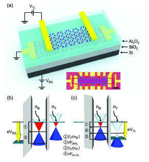
To understand the layer resistivity dependence on gate and inter-layer bias, it is instructive to examine a band structure model which relates the applied and biases to the top () and bottom () layer densities [Figs. 1(b,c)]. The applied can be written as the sum of the electrostatic potential drop across the bottom SiO2 dielectric and the Fermi energy of the bottom layer:
| (1) |
represents the Fermi energy of graphene relative to the charge neutrality (Dirac) point at a carrier density ; and are positive (negative) for electrons (holes). is the SiO2 dielectric capacitance per unit area. Similarly, an applied can be written as the sum of the electrostatic potential drop across the Al2O3 dielectric, and the Fermi energy of the two layers:
| (2) |
A positive applied on the top layer induces electrons (holes) in the bottom (top) layer, which explains the negative sign for the right hand side terms in Eq. (2). While the above equations implicitly assume that the two graphene layers are charge neutral at V, a finite doping of the two layers can be included in the above model using additive constants to the left hand side in Eqs. (1,2). Alternatively, and can be referenced with respect to the bias values which render both layers charge neutral, a convention which we adopt in discussing our experimental results [22].
3 Magnetotransport properties of individual layers
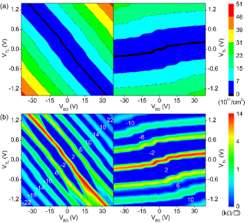
Figure 2(a) data show contour plots of and calculated according to Eqs. (1,2), with the following dependence of the Fermi energy on density , consistent with masseless particles with a Fermi velocity . The bottom SiO2 dielectric capacitance is nFcm-2, a value determined experimentally by probing the capacitance of metal pads located in proximity of the graphene double layer and confirmed by Hall measurements. The inter-layer capacitance value used here is nFcm-2 [23], and the Fermi velocity cm/s. Figure 2(a) data show that the charge neutrality point of the bottom layer follows an almost linear dependence on and , while the density of the top layer is controlled primarily by the inter-layer bias, and to a much lesser extent by the back-gate bias. To better understand these observations, let us first neglect in Eqs. (1,2): is controlled by only, and depends linearly on and , with and respectively as proportionality coefficients. Although this behavior resembles Fig. 2(a) data, noticeable departures can be observed as a result of the reduced density of states in graphene, and consequently non-negligible . First, does depend on , implying an incomplete screening of the back-gate induced electric field by the bottom layer, or equivalently a finite density of the states in the bottom layer, hence finite . Second, the line shows a noticeable non-linearity as a function of and near zero gate bias, a consequence of the non-negligible Fermi energy of the top layer.
Figure 2(b) data show contour plots of the longitudinal resistivities (left panel) and (right panel) measured in the bottom and top layers, respectively, at a temperature K. A comparison with Fig. 2(a) data reveals a very good agreement between the experimental data and calculations, validating the model of Eqs. (1,2). Interestingly, this model can be used to make a direct measurement of the Fermi energy in graphene, by employing one of the two layers as a resistively detected Kelvin probe [19]. Indeed, setting in Eq. (2) yields . The latter relation implies that the inter-layer bias required to bring the top layer to the charge neutrality point is equal to the Fermi energy of the bottom layer expressed in units of eV. Consequently, tracking the top layer charge neutrality point in Fig. 2(b) (right panel) yields the bottom layer Fermi energy as a function of .
We next address the layer density dependence on and in a perpendicular magnetic field (). In the presence of a -field the electrons occupy Landau levels (LL) with energies , where is an integer denoting the LL index. Including the spin and valley degrees of freedom each LL has a degeneracy of . Quantum Hall states (QHSs) develop at filling factors . Neglecting LL disorder-induced broadening, the Fermi energy dependence on density therefore writes , where and is the nearest integer function. Figure 3(a) data show contour plots of (left panel) and (right panel) calculated as a function of and at T using Eqs. (1,2), along with the same capacitance values used in Fig. 2(a): nFcm-2, nFcm-2. In addition, a finite broadening is assumed for each LL using a Lorentzian density of states distribution with a width meV for the LL and meV for [19].
Figure 3(b) data show the measured (left panel) and (right panel) as a function of and in sample 1, at K. The data display alternating regions of vanishing resistivity corresponding to quantum Hall states, and high resistivity regions corresponding to half filled LLs. A comparison with Fig. 3(b) data reveals a very good agreement of the charge neutrality point dependence on and for both layers, effectively validating Eqs. (1,2) model in high magnetic fields. Similar to Fig. 2(b) data, the value when the top layer is charge neutral is equal to the Fermi energy of the bottom layer. Consequently, the top layer charge neutrality line of Fig. 2(b) traces the bottom layer Fermi energy as a function of , and shows the staircase dependence corresponding to discrete LLs.
4 Coulomb drag of massless fermions in graphene
An important attribute of a double layer system is the ability to probe the Coulomb drag between the two layers. A charge current () flown in one (drive) layer results in a net momentum transfer to the opposite (drag) layer, thanks to the Coulomb interaction between electrons in the two layers. If no current is allowed to flow in the drag layer, a voltage builds up in order to counter the momentum transfer. The drag resistivity is defined as , where and are the length and width of the sample area over which the drag voltage is measured. In effect, the drag resistivity is proportional to the scattering rate between electrons located in opposite layers. The dependence of on , , , and the spacing between the two layers can provide insight into the interaction between the two layers, as well as the ground state in individual layers.
Coulomb drag between closely spaced carrier systems has been probed in a variety of GaAs/AlGaAs heterostructures which, depending on the type of sample used, allowed experimental access to electron-electron drag [24, 25], hole-hole drag [26], and electron-hole drag [27, 11, 12]. Assuming that the ground state in each layer is a Fermi liquid, and that the layer spacing is sufficiently large such that the Fermi wave-vector , the drag resistivity depends on the layer densities, temperature, and spacing as .
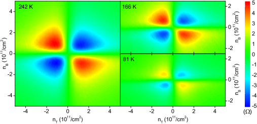
In Fig. 4 we show contour plots of as a function of , and , measured in sample 1 at different temperatures. The data were measured by flowing current in the bottom layer, and measuring the drag voltage in the top layer as a function of and , which were subsequently converted into layer densities using Eqs. (1,2). We note that because the drag voltage is orders of magnitude smaller than the longitudinal voltage drop in the drive layer, very small inter-layer leakage currents can introduce artifacts in the experimental data; care was taken here to ensure the measured drag voltage is not affected by inter-layer leakage. Figure 4 data explore in the four quadrants of the plane, and reveals several noteworthy findings. First, is negative (positive) for same (opposite) carrier polarity. Second, increases with increasing . Third, vanishes at large values, and in the vicinity of the points. Lastly, the vs. data in different quadrants are very similar, except for the sign change depending on the carrier type. As we explain below all these observations are consistent with Coulomb drag of masseless fermions where the ground state in each layer is a Fermi liquid.
Several theoretical studies examined the Coulomb drag in graphene to date [28, 29, 30, 31, 32, 33, 34]. In the weak-coupling limit, defined as , the drag resistance scales as [28, 32, 33, 34]
| (3) |
In the strong-coupling limit, defined as , is expected to have a weaker dependence on layer density, and to be independent of the layer spacing as [33, 34]
| (4) |
A close examination of Fig. 4 data reveals a -dependence which is stronger than , but weaker than , in the -range probed here. A best fit to vs. along the diagonals , and yields , with an exponent little dependent on temperature. The -value is lower than , expected in the weak-coupling limit, but larger than 1 expected in the strong-coupling limit. This can be readily understood since varies between 0.4 and 1 in the density range where is not vanishingly small. At low densities, where disorder-induced puddles in the two layers lead to a decrease of towards zero. The experimental dependence on , , and is in good agreement with the expected theoretical dependence of diffusive Coulomb drag in the Fermi liquid regime, although a quantitative matching between experiment and theory remains to be established.
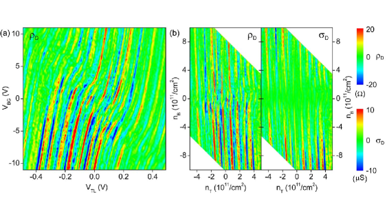
As the temperature is reduced below 50 K, the drag resistivity reveals a dramatic departure from the diffusive Coulomb drag of Fig. 4. In Fig. 5(a) we show a contour plot of measured as a function of and , at K in sample 2, and using the top (bottom) layer as the drag (drive) layer. Unlike the diffusive Coulomb drag of Fig. 4, the data of Fig. 5(a) show a pattern of large fluctuations centered around a zero average. The mesoscopic fluctuations increase in amplitude with reducing , and completely obscure the diffusive drag at low temperatures [18]. The mesoscopic fluctuations emerge as a result of phase coherent transport at low temperature, and represent the counterpart of universal conductance fluctuations in Coulomb drag [35]. Similar mesoscopic fluctuations have been observed in Coulomb drag probed between two-dimensional electron systems in GaAs/AlGaAs heterostructures, albeit at lower temperatures [36].
A comparison of Fig. 5(a) data with the carrier density contour plot of Fig. 2(a) calculations reveal an interesting observation. The locus of constant in Fig. 5(a) corresponds to the lines of constant in the plane of Fig. 2(a). Alternatively stated, the mesoscopic fluctuations track the drag layer constant density lines in the plane. To better illustrate this observation in Fig. 5(b) (left panel) we show a contour plot of vs. ; these data represent Fig. 5(a) data with axes converted into using Eqs. (1,2). The right panel of Fig. 5(b) (right panel) shows the drag conductivity vs. . We note that the fluctuation amplitude has the same order of magnitude as . Figure 5(b) data manifestly show that the Coulomb drag mesoscopic fluctuations depend mainly on the drag layer density (), and are largely insensitive to the drive layer density (). This observation is manifestly at variance with the Onsager reciprocity relation, according to which interchanging the drag and drive layers should not affect the measured .
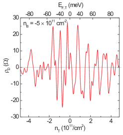
Examination of Fig. 5(b) data reveals a regular, almost periodic vs. pattern. To better illustrate this pattern, in Fig. 6 we show vs. measured at a fixed drive layer density, cm-2, and at K. The data reveals an almost periodic dependence of vs. reminiscent of Fabry-Perot interference [37]. A simple analysis can relate the top layer Fermi energy () change corresponding to maxima to a cavity length (), via . A typical value for of 10 meV deduced from Fig. 6 data, corresponds to m, a value comparable to the phase coherence length in graphene on SiO2 [38] at K.
5 Conclusions
In summary, we present a magnetotransport and Coulomb drag study in graphene double layers, consisting of two independently contacted graphene monolayers separated by a thin Al2O3 dielectric. The Coulomb drag probed in this system reveals two regimes: (i) diffusive drag at elevated ( K) temperatures, and (ii) mesoscopic fluctuations dominated drag at low temperatures. The temperature dependence of the diffusive drag is consistent with the Fermi liquid theory, while the density dependence suggests the layers are close to the strong-coupling regime [33, 34]. The Coulomb drag mesoscopic fluctuations observed at low temperature depend mainly on the drag layer density, and are largely insensitive to the drive layer density, an observation which is at variance with the Onsager reciprocity relation.
We thank A. H. MacDonald, B. Narozhny, N. M. R. Peres, W.-K. Tse, S. K. Banerjee, and L. F. Register for discussions. We gratefully acknowledge support from ONR, NRI, and NSF (DMR-0819860).
References
- [1] Y.W. Suen, L.W. Engel, M.B. Santos, M. Shayegan, and D.C. Tsui, Phys. Rev. Lett. 68, 1379 (1992).
- [2] J.P. Eisenstein, G.S. Boebinger, L.N. Pfeiffer, K.W. West, and S. He, Phys. Rev. Lett. 68, 1383 (1992).
- [3] D. R. Luhman, W. Pan, D. C. Tsui, L. N. Pfeiffer, K. W. Baldwin, and K. W. West, Phys. Rev. Lett. 101, 266804 (2008).
- [4] J. Shabani, T. Gokmen, M. Shayegan, Phys. Rev. Lett. 103, 046805 (2009).
- [5] Kun Yang, K. Moon, L. Zheng, A.H. MacDonald, S.M. Girvin, D. Yoshioka, and S.C. Zhang, Phys. Rev. Lett. 72, 732 (1994); K. Moon, H. Mori, Kun Yang, S.M. Girvin, A.H. MacDonald, L. Zheng, D. Yoshioka, and S.C. Zhang, Phys. Rev. B 51, 5138 (1995).
- [6] I.B. Spielman, J.P. Eisenstein, L.N. Pffeifer, and K.W. West, Phys. Rev. Lett. 84, 5808 (2000).
- [7] M. Kellogg, J.P. Eisenstein, L.N. Pffeifer, and K.W. West, Phys. Rev. Lett. 93, 036801 (2004).
- [8] E. Tutuc, M. Shayegan, and D.A. Huse, Phys. Rev. Lett. 93, 036802 (2004).
- [9] J. P. Eisenstein, and A. H. MacDonald, Nature 432, 691 (2004).
- [10] Y. E. Lozovik, V. I. Yudson, JETP Lett. 22, 274 (1975).
- [11] A. F. Croxall et al., Phys. Rev. Lett. 101, 246801 (2008).
- [12] J. A. Seamons, C. P. Morath, J. L. Reno, M. P. Lilly, Phys. Rev. Lett. 102, 026804 (2009).
- [13] K. S. Novoselov et al., Science 306, 666 (2004).
- [14] K. S. Novoselov et al., Nature 438, 197 (2005).
- [15] Y. Zhang et al., Nature 438, 201 (2005).
- [16] H. Min, R. Bistritzer, J.-J. Su, A. H. MacDonald, Phys. Rev. B 78, 121401 (2008).
- [17] C.-H. Zhang, Y. N. Joglekar, Phys. Rev. B 77 233405 (2008).
- [18] S. Kim et al., Phys. Rev. B 83, 161401 (2011).
- [19] S. Kim et al., Phys. Rev. Lett. 108, 116404 (2012).
- [20] L. A. Ponomarenko et al., Nat. Phys. 7, 958 (2011).
- [21] L. Britnell et al., Science 335, 947 (2012).
- [22] The the bias values at which both layers are at the Dirac point are V, V for sample 1, and V, V for sample 2.
- [23] The ratio is determined from the slope of the bottom layer charge neutrality point traced as a function of and . is determined using the ratio and the measured value. We note that consists of the Al2O3 dielectric capacitance plus series contributions associated with the graphene-dielectric interfaces; B. Fallahazad et al., Appl. Phys. Lett. 100, 093112 (2012).
- [24] P. M. Solomon, P. J. Price, D. J. Frank, D. C. La Tulipe, Phys. Rev. Lett. 63, 2508 (1989).
- [25] T. J. Gramila, J. P. Eisenstein, A. H. MacDonald, L. N. Pfeiffer, K. W. West, Phys. Rev. Lett. 66, 1216 (1991).
- [26] R. Pillarisetty et al., Phys. Rev. Lett. 89, 016805 (2002).
- [27] U. Sivan, P. M. Solomon, H. Shtrikman, Phys. Rev. Lett. 68, 1196 (1992).
- [28] W.-K. Tse, B. Y.-K. Hu, S. Das Sarma, Phys. Rev. B 76, 081401 (2007).
- [29] B. N. Narozhny, Phys. Rev. B 76, 153409 (2007).
- [30] N. M. R. Peres, J. M. B. Lopes dos Santos, A. H. Castro Neto, Europhys. Lett. 95, 18001 (2011).
- [31] E. H. Hwang, R. Sensarma, S. Das Sarma, Phys. Rev. B 84, 245441 (2011).
- [32] M. I. Katsnelson, Phys. Rev. B 84, 041407 (2011).
- [33] B. N. Narozhny, M. Titov, I. V. Gornyi, P. M. Ostrovsky, Phys. Rev. B 85, 195421 (2012).
- [34] M. Carrega, T. Tudorovskiy, A. Principi, M. I. Katsnelson, M. Polini, arXiv:1203.3386 (2012).
- [35] B. N. Narozhny, I. L. Aleiner, Phys. Rev. Lett. 84, 5383 (2000).
- [36] A. S. Price, A. K. Savchenko, B. N. Narozhny, G. Allison, D. A. Ritchie, Science 316, 99 (2007).
- [37] A. F. Young, P. Kim, Nat. Phys. 5, 222 (2009).
- [38] J. Berezovsky and R. M. Westervelt, Nanotechnology 21, 274014 (2010).