Scanning superconducting quantum interference device on a tip for magnetic imaging of nanoscale phenomena
Abstract
We describe a new type of scanning probe microscope based on a superconducting quantum interference device (SQUID) that resides on the apex of a sharp tip. The SQUID-on-tip is glued to a quartz tuning fork which allows scanning at a tip-sample separation of a few nm. The magnetic flux sensitivity of the SQUID is 1.8 and the spatial resolution is about 200 nm, which can be further improved. This combination of high sensitivity, spatial resolution, bandwidth, and the very close proximity to the sample provides a powerful tool for study of dynamic magnetic phenomena on the nanoscale. The potential of the SQUID-on-tip microscope is demonstrated by imaging of the vortex lattice and of the local AC magnetic response in superconductors.
pacs:
85.25.Dq, 07.79.Lh, 74.25.QtI Introduction
Within the rapidly developing field of nanotechnology there is a growing need for highly sensitive imaging techniques of local magnetic fields on the nanoscale Bending-1999 ; Kirtley2010 ; Degen2009 ; Gierling2011 ; Grinolds2011 ; Balasubramanian2008 . The magnetic force microscopy Moser-1995 ; Schwarz2008 and Lorentz microscopy Tonomura-1999 offer very high spatial resolution but lack in their field sensitivity. Conversely, scanning superconducting quantum interference device (SQUID) microscopes have the highest field sensitivity, but they currently suffer from rather low spatial resolution Kirtley2010 . In order to overcome this limitation, in recent years there is a growing interest in micro and nanoSQUIDs Foley2009 ; CleuziouJ.-P.2006 ; koshnick:243101 ; Nagel2011 ; lam:1078 ; PhysRevB.70.214513 ; hao:092504 ; Nb_nanoSQUID ; Lam-2011 ; Granata2008 . Since the magnetic field of a nanostructure decays rapidly with distance, the measured spatial resolution is ultimately limited by the separation between the sample and the probe. In order to achieve nm scale resolution, the probe has to be able to approach and scan the sample within a few nm of the surface. One of the obstacles towards this goal is the location of the SQUID itself, i.e., on a wafer or chip, making it difficult to bring the sensor (or the pick-up loop, if separate from the sensor) closer than a few hundred nanometers to the sample. The main challenge is therefore to develop magnetic field sensors that have high field sensitivity, very small dimensions, and a compatible geometry.
In this paper we describe a new scanning probe microscope (SPM). The innovative element of the instrument is a nanoSQUID that resides on a sharp tip Finkler2010 , which is ideally suited for scanning microscopy. By attaching the SQUID-on-tip (SOT) to a quartz tuning fork (TF) we can scan the sensor within few nm from the surface of the sample, thus providing a quantitative, high sensitivity, and high spatial resolution tool for imaging and investigation of static and dynamic magnetic phenomena on the nanoscale. The feasibility of the method is demonstrated by imaging of the vortex lattice and of the local DC and AC magnetic response in Al, NbSe2 and Nb superconductors. In addition, we present nanoscale topography imaging capability of the microscope along with the magnetic imaging.
II Instrumentation
II.1 SQUID-on-tip
II.1.1 Fabrication
Using a commercial pipette puller Note1 , we pull a quartz tube with 1 mm outer diameter and an inner diameter of 0.5 mm to form a pair of sharp pipettes with a tip diameter that can be controllably varied between 100 and 400 nm. Then, we either solder a thin layer of indium or evaporate a 200 nm-thick film of gold on two sides of the cylindrical base of the pipette. Afterwards, the pipette is mounted on a rotator and put into a vacuum chamber for three steps of thermal evaporation of aluminum. The rotator (see Fig. 1a) has an electrical feedthrough for two operations. First, a 2 mW red laser diode is mounted colinear with the tip, which is used to point the tip towards the very center of the source. This defines the zero angle. The second electrical connection is for an in situ measurement of the tip’s resistance during deposition. In the first step, 25 nm of aluminum are deposited on the tip tilted at an angle of -100∘. Then the tip is rotated to an angle of +100∘ for a second deposition of 25 nm, as shown in Fig. 1b.
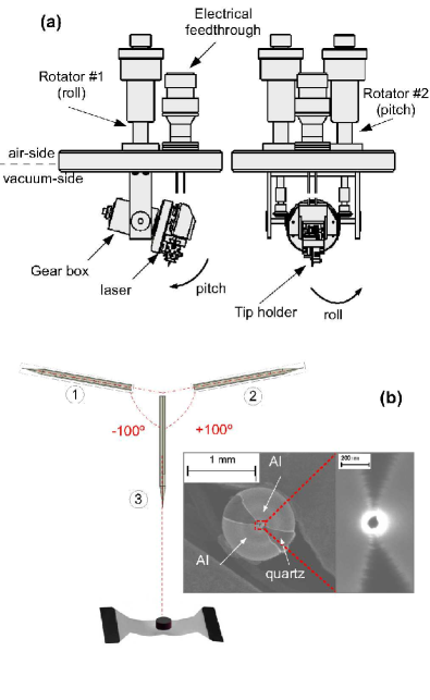
As a result, two leads are formed on opposite sides of the quartz tube separated by gap regions of bare quartz. In the last step, 20-22 nm of aluminum are deposited at an angle of 0∘, coating the apex ring of the tip. Due to geometrical considerations, in this step about 3 nm of aluminum are also deposited in the gap regions at a very shallow deposition angle. This thin layer, however, does not percolate and hence does not short the two leads. The resulting structure is therefore a ring connected to two leads (see inset in Fig. 1b). “Strong” superconducting regions are formed in the areas where the leads make contact with the ring, while the two parts of the ring in the region of the gap between the leads constitute two weak links, thus forming the SQUID. A finite resistance appears after depositing approximately 7 nm in the third step. The typical final room-temperature resistance of the SOT is 1.5 k. Since the device is highly sensitive to electrostatic discharge (ESD), we follow a strict protocol of anti-ESD procedures, which include, among others, the use of grounding strips, mats and physical electrical shorts on the tip during transfer.
II.1.2 Characterization
A series SQUID array amplifierHuber-2001 (SSAA) is used as a cryogenic current-to-voltage converter to read out the SOT. The SOT is connected in a voltage-bias configuration, as shown in Fig. 2a.
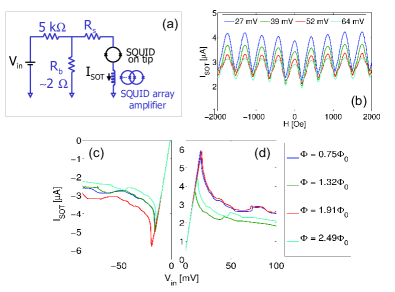
For each value of the applied magnetic field, , we measure the current through the SOT, , as a function of the input voltage, . At low , the SOT is in its superconducting state, and is linear with . At mV, the SOT switches to its voltage state and a decrease in the current through it is observed, plotted in Figs. 2c and 2d. At higher values of , the SOT behaves again as a resistive element. Similary, Fig. 2b shows the SOT response upon sweeping the applied field at various constant biases. After mapping the entire space and measuring the current noise in each point in that space, we choose a working point of and , at which the ratio between the noise (in units of A/Hz1/2) and the sensitivity, (in units of A/Oe) is minimal. Since the response is periodic in field, and since our SOTs are usually asymmetric Finkler2010 with respect to applied field and polarity of , there is a wide range of fields and polarities at which high sensitivity can be achieved. After choosing a working point, we perform a calibration measurement to determine the exact G/A converstion ratio.
II.2 Tuning-fork microscopy
II.2.1 Assembly
Commercial quartz tuning forks (TF), normally used as time bases in digital watches, are employed as force sensors. They are laser-trimmed to have a resonance at Hz, and typically have a high Q-factor due to low internal losses (dissipation) in quartz. We glue the SOT to one prong of the TF, whose length is 4 mm, width 0.6 mm and thickness 0.34 mm (Figs. 3a and 3b). When the SOT approaches the surface of the sample, electrostatic and van der Waals forces dampen the TF’s resonance and shift its frequencyGiessibl . Tuning fork microscopy uses either the decrease in amplitude or the change in frequency as the feedback parameter. In our setup we monitor the frequency shift of the TF using a phase-locked loop (PLL). We can detect a small frequency increase at about 20 nm from the surface that grows on approaching the surface. At 10 nm from the sample surface the increase of the TF resonant frequency is typically about 100 mHz. Preparing a TF for microscopy entails the removal of its vacuum can and the two wires soldered to its contacts. It is then glued to a 550.5 mm3 quartz piece which was pre-coated with two gold pads (70 Å Cr/2000 Å Au). Alternatively, this quartz piece is replaced by a dither piezo having the same dimensions (shown in Fig. 3c). The two TF contacts are wire-bonded to those gold pads, which are in turn connected to external wires via two additional wire bonds.
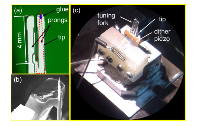
One can electrically excite the TF with a voltage source and read the current through it using a current-to-voltage converter grober:2776 . However, it is more advantageous to decouple the excitation from the readout by using the voltage source to drive the dither piezo, which mechanically excites the TF. This latter method reduces the effect of stray capacitances of the cables and the electrical contacts themselves from entering the readout signal. We used a shear-dither piezo Note2 for this purpose, which was used both as the plate to which we glued the TF and as its mechanical excitation medium (shown in Fig. 3c).
II.2.2 Tip-sample interaction and electronics
In our microscope setup, as shown in Fig. 3c, the tip is positioned between two stainless steel electrodes, such that each SOT lead is in contact with one of the two. External wires are soldered to the electrodes to provide electrical contact to the SOT. We glue the SOT to one of the prongs of the TF. This dampens the resonance Shelimov2000 dramatically. Therefore, we try to use as small an amount of glue as possible. Using a two-part epoxy with an extremely low viscosity (150 mPas) enables us to place a very small drop of glue (Fig. 3b). The farther the SOT protrudes above the edge of the prong, the smaller its effective spring constant Karrai2000 becomes (for a cylindrical tip):
where , and are the radius, length and Young modulus of the tip, respectively. Thus, if the SOT protrudes too much, the electrostatic forces of interaction with the sample will dampen its motion while the tuning fork’s prong remains almost unaffected. Consequently, we always try to position the tip with respect to the tuning fork so that the SOT itself protrudes only slightly above the edge of the prong (typically a few tens of microns). We then excite the tuning fork and measure its resonance, specifically noting the location of the peak, its amplitude and its width. This measurement is performed at room temperature and atmospheric pressure and repeated at low temperature (300 mK) in vacuum for comparison. Typical resonance curves for the TF at room temperature and low temperature are plotted in Fig. 4.
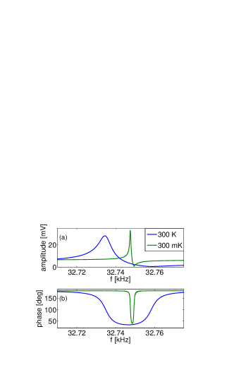
More often than not, the low temperature, high vacuum resonance of the tuning fork is much sharper than at room temperature and atmospheric pressure. One can monitor the height of the resonance peak and set the feedback threshold to, for example, 50% of the maximum. This method, also known as slope detection Albrecht , is not fast enough, since quartz tuning forks have relatively high Q-factors, especially at low temperatures (typically a few 100,000 for a bare TF and a few 10,000 for a TF glued to a tip) Albrecht ; durig:3641 . These high Q-factors result in a long settling time, of the order of seconds, which is unacceptable for scanning probe microscopy. We have used a phase-locked loop (PLL, either RHK’s PLLpro or attocube’s ASC500) to increase the bandwidth and scanning speed Albrecht ; Gildemeister . Interaction forces between the tip and the sample result in a frequency shift of the tuning fork’s resonance. The basic idea behind the PLL is to track this resonance in a closed loop circuit and compare its current location with the fundamental one to give the frequency shift, . This frequency shift serves as the error function of the height, or , feedback loop and hence allows simultaneous imaging of the magnetic field and sample topography. In our setup, the typical scanning speed was between 0.5-1 /sec when using the PLL.
II.3 Microscope design
The microscope assembly, described below, is mounted on a 3He Oxford HelioxTL probe, which was modified for this purpose. It is designed to work in vacuum at a base temperature of less than 300 mK. All crucial signals (SSAA, tuning fork, SOT) are transmitted via coaxial cables, while the rest are passed through either Manganin or NbTi twisted-pairs in order to reduce the heat load from room temperature.
II.3.1 Schematics of the assembly
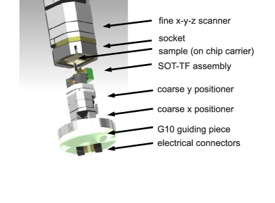
The coarse motion is performed by three attocube Note3 positioners (1ANPz101RES, 2ANPx50), one for each axis, based on the slip-stick mechanism. The positioners themselves are driven by a saw tooth pulse from a high-voltage driver (attocube ANC-150). The z-axis positioner incorporates a resistive encoder that gives its absolute position to an accuracy of 2 m and resolution of 200 nm. Scanning is performed by an attocube integrated xyz scanner (ANSxyz100), with an x-y scan range of and a z-scan range of 15 , all at mK. The microscope is shown in Fig. 5.
We drive these piezoelectric scanners with voltage from an SPM controller (either RHK SPM-100 or attocube ASC500). As mentioned above, the output of the PLL (in the form of a frequency shift, ) serves as the input of the z-height feedback loop. This feedback loop controls the height of the tip above the sample by changing the voltage applied to the z-scanner.
II.3.2 Vibration/isolation and acoustics considerations
The cryostat was isolated from floor vibrations by suspending it in the center of a hollow marble block supported by four commercial isolators Note4 ; the weight of the marble is 920 kg. These isolators attenuate vibrations from the environment at low frequencies, (-20 dB at 10 Hz). The disadvantage of these isolators is that they have a resonance at around 1 Hz. To reduce acoustical noise, we wrapped the dewar with an acoustic blanket Note5 that attenuated the vibrations of the dewar’s outer vacuum chamber by 3 dB at its resonance frequency of 186 Hz. In addition, the top of the cryostat was covered by an acoustic enclosure Note6 that sits on the marble and seals well to its smooth surface. The enclosure provides further attenuation of 45 dB at 500 Hz. The combination of the isolators and the enclosure created a sufficiently quiet environment in which we were able to safely scan samples with the tip-sample separation of a few nanometers.
III Measurements
With its magnetic sensor coupled to a topography sensor, the scanning SQUID microscope can acquire simultaneously both the topography and magnetic signals of the sample. Below we present measurements of three different types of samples, exhibiting the potential of the instrument.
III.1 Self-induced magnetic field of a transport current
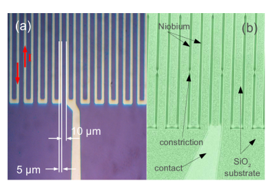
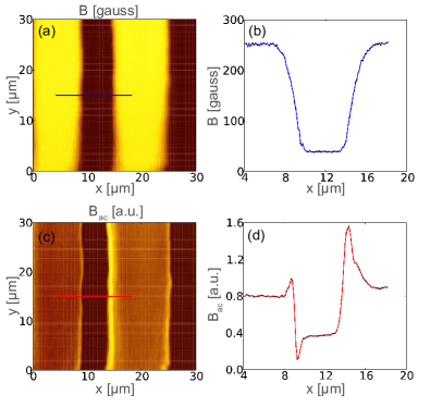
Our first calibration sample was an aluminum serpentine, 200 nm thick, with a line width of 5 and a period of 15 (see Fig. 6a).
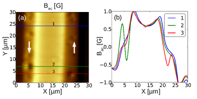
Already at a distance of 10 m from its surface, the SOT was able to image the AC magnetic field generated by an AC current of 2 mA in the serpentine. Figure 7 shows the self-induced field due to two adjacent strips of the serpentine, measured in constant height mode without feedback on . Following Biot-Savart law in superconducting strip geometry Zeldov1994 , the AC transport current in the left strip gives rise to a positive (in-phase) field on the right edge of the strip and a negative (out-of-phase) signal on the left edge. The adjacent strip, carrying current in the opposite direction, generates an inverted field profile. The resulting combined field is high in-between the strips (bright color) and low (dark) outside the strips. In addition, we resolve fine structure within the strips. Since our Al film is type-I superconductor, small normal regions are formed in the central part of the strips in the presence of applied DC field of 90 Oe. The applied transport current flows only in the superconducting regions, avoiding the normal areas, giving rise to the “depressions” in the local AC field.
III.2 Magnetic screening in a NbSe2 crystal
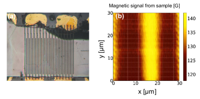
Aluminum, being a type-I superconductor, does not exhibit vortices and therefore one cannot observe them in thick films of such a material. In order to investigate type-II superconductors we have prepared serpentines of NbSe2 single crystal and of Nb thin films. A 10 m thick cleaved NbSe2 crystal was milled using a focused ion beam (FIB) to a serpentine shape as shown in Fig. 8a. The sample was cooled in a low field and then the applied field was increased to 140 Oe. The local magnetic field was then imaged at a height of 2.5 m above the surface of the serpentine as shown in Fig. 8b. The screening currents partially shield the magnetic field in the NbSe2 strips (dark) and enhance the field in-between the strips (bright).
III.3 Vortex matter in thin niobium films
Nb film was deposited on a Si substrate using an e-gun while keeping the substrate at a temperature of 300 ∘C in a background pressure of Torr. The 200 nm-thick film was patterned into a serpentine structure as shown in Fig. 6b. The sample was cooled in a small residual field, then the applied field was increased and the local magnetic field was imaged by the scanning SOT at 250 Oe, as shown in Figs. 9a and 9b. The dark regions are the Nb strips that are essentially fully screened due to very strong vortex pinning in Nb films at low temperatures.
In order to demonstrate operation of the SOT at high frequencies we take advantage of the fact that the TF and the tip oscillate at 32 kHz in the plane parallel to the sample surface. In presence of a field gradient this oscillation gives rise to an effective AC magnetic field as sensed by the SOT, , where is the amplitude of the tip oscillation along the axis. We can vary from below a nm to few tens of nm. Using a lock-in amplifier we can thus measure simultaneously the DC and the AC magnetic signals while scanning the sample. Figure 9 shows an example of such simultaneous measurement of and at 32 kHz in a Nb serpentine scanned a few microns above the sample in constant height mode, in a DC field of 250 Oe.
Finally, we demonstrate the high spatial resolution of the instrument by imaging vortices and surface topography in Nb film. For this the same sample was field-cooled in an applied magnetic field of 20 Oe and the scanning was carried out in a closed feedback mode in which the tip maintains a constant height of few nm above the surface. Three signals are measured and imaged simultaneously during the scan: the DC SOT signal which provides , the AC SOT signal at 32 kHz which reflects the , and the feedback voltage which renders the sample topography. Figures 10a and 10b show vortices imaged in the Nb film by the DC and AC magnetic signals.
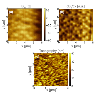
The observed vortex lattice is highly disordered due to very strong pinning in Nb film at 300 mK (see Ref. Brandt-1995, and references therein). In the DC image the vortices are visible as bright spots, while in the AC image the vortices appear as a bright-dark pairs from left to right as determined by the field gradient. We can fit the spatial field dependence of the individual vortices to theoretical calculations Brandt2005 to find the corresponding magnetic penetration depth in the Nb film, which in this case turns out to be 400 nm. In the image area of there are about 34 individual vortices, corresponding to an average field of 14 G, in fair agreement with the applied field. Figure 10c shows a high resolution topographical image of the sample (in a different scan area), showing the granular structure of the Nb film. Most grains are 120 to 300 nm in diameter and 25 to 35 nm in height.
IV Summary and future prospects
We described a new scanning nanoSQUID microscope based on the development of a unique SQUID-on-tip. The unconventional geometry of the SQUID-on-tip together with the coupling to a quartz tuning fork allows for its assembly as a dual magnetic/topographic scanning probe microscope, making it the first SQUID acting as magnetic sensor in a scanning probe microscope with the sensor itself being only a few nanometers away from the surface of the sample. Since in most of the relevant microscopic systems the magnetic signal decays rapidly with the distance from the sample (distance cubed for magnetic dipoles, exponentially for a vortex lattice in superconductors, etc.), achievement of such a close sensor-sample separation is of major importance. The potential of the instrument has been demonstrated by study of DC and AC magnetic phenomena in type-I and type-II superconductors, including imaging the self-induced magnetic field of an AC transport current in Al thin films, observation of the magnetic shielding in NbSe2 single crystal and in Al and Nb films, and imaging of disordered vortex lattice along with nanoscale surface topography in Nb films. In addition, the SQUID-on-tip is expected to become a very sensitive probe of magnetic dipoles due to its high flux sensitivity and very small size. Currently the projected Tilbrook2009 spin sensitivity of our Al SQUID-on-tip is 65 and there is a strong potential for development of more sensitive variations of the device towards the goal of single spin sensitivity. The scanning SQUID-on-tip microscope is thus a promising tool for study of a wide range of static and dynamic magnetic phenomena on the nanoscale.
We acknowledge fruitful discussions with Shahal Ilani, Grigorii Mikitik, Ernst H. Brandt and Daniel Prober. This work was supported by the European Research Council (ERC) Advanced Grant, by the German-Israeli Foundation (GIF), and by the U.S.-Israel Binational Science Foundation (BSF).
References
- (1) S. J. Bending, Adv. Phys. 48, 449 (1999).
- (2) J. R. Kirtley, Rep. Prog. Phys. 73, 126501 (2010).
- (3) C. L. Degen, M. Poggio, H. J. Mamin, C. T. Rettner, D. Rugar, Proc. Natl. Acad. Sci. 106, 1313 (2009).
- (4) M Gierling, P. Schneeweiss, G. Visanescu, P. Federsel, M. Häffner, D. P. Kern, T. E. Judd, A. Günther, J. Fortágh, Nat. Nano. 6, 446 (2011).
- (5) M. S. Grinolds, P. Maletinsky, S. Hong, M. D. Lukin, R. L. Walsworth, A. Yacoby, Nat. Phys. 7, 687 (2011).
- (6) G. Balasubramanian, I. Y. Chan, R. Kolesov, M. Al-Hmoud, J. Tisler, C. Shin, C. Kim, A. Wojcik, P. R. Hemmer, A. Krueger, T. Hanke, A. Leitenstorfer, R. Bratschitsch, F. Jelezko, J. Wrachtrup, Nature 455, 648 (2008).
- (7) A. Moser, H. J. Hug, I. Parashikov, B. Stiefel, O. Fritz, H. Thomas, A. Baratoff, H.-J. Güntherodt, and P. Chaudhari, Phys. Rev. Lett. 74, 1847 (1995).
- (8) A. Schwarz, R. Wiesendanger, Nano Today 3, 28 (2008).
- (9) A. Tonomura, H. Kasai, O. Kamimura, T. Matsuda, K. Harada, J. Shimoyama, K. Kishio, and K. Kitazawa, Nature 397, 308 (1999).
- (10) C. P. Foley and H. Hilgenkamp, Supercond. Sci. Technol. 22, 064001 (2009).
- (11) J.-P. Cleuziou, W. Wernsdorfer, V. Bouchiat, T. Ondarcuhu, and M. Monthioux, Nature Nanotech. 1, 53 (2006).
- (12) N. C. Koshnick, M. E. Huber, J. A. Bert, C. W. Hicks, J. Large, H. Edwards, and K. A. Moler, Appl. Phys. Lett. 93, 243101 (2008).
- (13) J. Nagel, O. F. Kieler, T. Weimann, R. Wölbing, J. Kohlmann, A. B. Zorin, R. Kleiner, D. Koelle, and M. Kemmler, Appl. Phys. Lett. 99, 032506 (2011).
- (14) S. K. H. Lam and D. L. Tilbrook, Appl. Phys. Lett. 82, 1078 (2003).
- (15) C. Veauvy, K. Hasselbach, and D. Mailly, Phys. Rev. B 70, 214513 (2004).
- (16) L. Hao, C. A. Mann, J. C. Gallop, D. Cox, F. Ruede, O. Kazakova, P. Josephs-Franks, D. Drung, and T. Schurig, Appl. Phys. Lett. 98, 092504 (2011).
- (17) A. G. P. Troeman, H. Derking, B. Borger, J. Pleikies, D. Veldhuis, and H. Hilgenkamp, Nano Lett. 7, 2152 (2007).
- (18) S. K. H. Lam, J. R. Clem, and W. Yang, Nanotechnology 22, 455501 (2011).
- (19) C. Granata, E. Esposito, A. Vettoliere, L. Petti, and M. Russo, Nanotechnology 19, 275501 (2008).
- (20) A. Finkler, Y. Segev, Y. Myasoedov, M. L. Rappaport, L. Ne’eman, D. Vasyukov, E. Zeldov, M. E. Huber, J. Martin, and A. Yacoby, Nano Lett. 10, 1046 (2010).
- (21) Sutter Instruments P-2000.
- (22) M. J. Yoo, T. A. Fulton, H. F. Hess, R. L. Willett, L. N. Dunkleberger, R. J. Chichester, L. N. Pfeiffer, and K. W. West, Science 276, 579 (1997).
- (23) M. Huber, P. Neil, R. Benson, D. Burns, A. Corey, C. Flynn, Y. Kitaygorodskaya, O. Massihzadeh, J. Martinis, and G. Hilton, IEEE Trans. Appl. Supercond. 11, 4048 (2001).
- (24) F. J. Giessibl, Rev. Mod. Phys. 75, 949 (2003).
- (25) R. D. Grober, J. Acimovic, J. Schuck, D. Hessman, P. J. Kindlemann, J. Hespanha, A. S. Morse, K. Karrai, I. Tiemann, and S. Manus, Rev. Sci. Instrum. 71, 2776 (2000).
- (26) EBL#4, http://www.eblproducts.com/leadzirc.html.
- (27) K. B. Shelimov, D. N. Davydov, and M. Moskovits, Rev. Sci. Instrum. 71, 437 (2000).
- (28) K. Karrai, in Lecture notes on shear and friction force detection with quartz tuning forks, Work presented at the ”Ecole Thématique du CNRS” on near field optics (2000).
- (29) T. R. Albrecht, P. Grütter, D. Horne, and D. Rugar, J. Appl. Phys. 69, 668 (1991).
- (30) U. Dürig, H. R. Steinauer, and N. Blanc, J. Appl. Phys. 82, 3641 (1997).
- (31) A. E. Gildemeister, T. Ihn, C. Barengo, P. Studerus, and K. Ensslin, Rev. Sci. Instrum. 78, 013704 (2007).
- (32) Attocube Systems AG, http://www.attocube.com.
- (33) Newport S-2000.
- (34) Palziv Acousti Pipe Premium 10.
- (35) HNA, http://www.hna.co.il.
- (36) E. Zeldov, J. R. Clem, M. McElfresh, and M. Darwin, Phys. Rev. B 49, 9802 (1994).
- (37) E. H. Brandt, Rep. Prog. Phys. 58, 1465 (1995).
- (38) E. H. Brandt, Phys. Rev. B 71, 014521 (2005).
- (39) D. L. Tilbrook, Supercond. Sci. Technol. 22, 064003 (2009).