Plasmon transport in graphene investigated by time-resolved measurement
N. Kumada1,∗, S. Tanabe1, H. Hibino1, H. Kamata1,2, M. Hashisaka2, K. Muraki1 and T. Fujisawa2
1NTT Basic Research Laboratories, NTT Corporation, 3-1 Morinosato-Wakamiya, Atsugi, Kanagawa, Japan
2Department of Physics, Tokyo Institute of Technology, 2-12-1 Ookayama, Meguro, Tokyo, Japan
Plasmons, which are collective charge oscillations, offer the potential to use optical signals in nano-scale electric circuits [1, 2, 3]. Recently, plasmonics using graphene [4, 5, 6, 7, 8] have attracted interest, particularly because of the tunable plasmon frequency through the carrier density [8, 9]. However, the dependence of the plasmon velocity is weak () and it is difficult to tune the frequency over orders of magnitude. Here, we demonstrate that the velocity of plasmons in graphene can be changed over two orders of magnitude by applying a magnetic field and by the presence/absence of a gate; at high , edge magnetoplasmons (EMPs), which are plasmons localized at the sample edge, are formed and their velocity depends on and the gate screening effect. The wide range tunability of the velocity and the observed low-loss plasmon transport encourage designing graphene nanostructures for plasmonics applications.
On metal surface, resonant interactions between electrons in nanoparticles and the electromagnetic field of light create surface plasmons. Since the wavelength of surface plasmons can be reduced to the size dimensions of electronic devices, plasmonics have been proposed to merge optics and electronics [1, 2, 3]. However, there are fundamental obstacles to use metals for plasmonics: plasmon properties cannot be tuned once the material and the device geometry are determined and the plasmon decay time is short ( fs). In graphene, theory has predicted that the dispersion of sheet plasmons changes with the carrier density as [9]. Recently, the tunable resonant frequency of sheet plasmons in graphene micro-ribbon structures have been demonstrated [8]. On the analogue of conventional two-dimensional systems in GaAs, edge magnetoplasmons (EMPs) are expected to be formed at high and the dispersion is also changed by applying [10, 11, 12, 13] and by the presence of a gate [14]. Furthermore, low-loss plasmon transport is expected [6] when the plasmon-electron [15, 16, 17] and plasmon-phonon [18, 19, 20] couplings are suppressed. These studies suggest that graphene is a promising candidate material for the plasmonics.
Here, we show that the velocity of plasmons can be tuned over a wide range between 2,500 and 10 km/s by and the gate using time-resolved transport measurements. In the absence of and a gate, the velocity is faster than the Fermi velocity km/s, evidence for the transport of sheet plasmons. In quantum Hall (QH) effect regime at high , the velocity decreases with the Hall conductance , indicating the formation of EMPs, which are plasmons confined in QH edge channels. In a sample with a gate, the screening effect reduces the velocity by one order of magnitude and changes the dependence of the EMP velocity. Since edge channels formed at high and p-n junctions [7, 21] formed by using gates are useful to guide plasmons, the wide-range tunability of the plasmon velocity using and a gate encourage designing graphene nanostructures for plasmonic circuits.
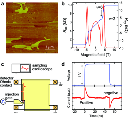
For this work, large-area graphene is essential to obtain long time of flight that can be resolved by electrical means. We prepared a graphene wafer by thermal decomposition of a 4H-SiC(0001) substrate [22]. The edge of graphene devices was defined by etching the graphene and the SiC substrate. The surface of the devices was covered with 100-nm-thick hydrogen silsequioxane (HSQ) and 40-nm-thick SiO2 insulating layers. As a result of n-doping from the SiC substrate and p-doping from the HSQ layer, graphene has n-type carriers with cm-2. Longitudinal and Hall resistances in a millimeter-scale Hall bar show well developed and 6 QH states (Fig. 1b), demonstrating that the carrier density is almost uniform even in the large device.
For the time-resolved transport measurement, we used two samples, one with and the other without a large top gate (Fig. 1c). Excited charges with the energy of meV are injected into graphene by applying a square voltage pulse to the injection gate deposited across the sample edge: at the rising and falling edges of the pulse, positive and negative charges are generated, respectively (Fig. 1d). The charges propagate in the sample and are detected as the time-dependent current by a sampling oscilloscope through the detector Ohmic contact, which is located 1.1 mm away from the injection gate. The origin of the time is set at the onset of the injection pulse (supplementary information). All measurements were performed at 1.5 K.
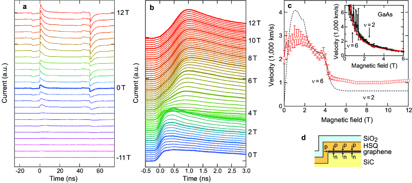
Figure 2 shows results for the sample without a top gate. The current traces are asymmetric with respect to T (Fig. 2a) because of the chirality of the edge current: when is applied from the back of the sample (), the chirality is clockwise and the injected charges travel to the detector Ohmic contact along the left edge (Fig. 1c); otherwise (), the charges flow to other grounded Ohmic contacts. For , detailed measurements with fine time and steps (Fig. 2b) reveal that the amplitude and the time delay of the current pulse depend on . The amplitude of the current pulse is large around T and for T, where the and QH states are formed, respectively. This indicates that the charge relaxation is mainly due to scattering by electrons in bulk graphene. The time delay at the current peak, which corresponds to the time of flight of charges, is about 1 ns. It increases with and becomes almost constant in the QH state for T [23].
The velocity of charges can be calculated from the time of flight and the length of the edge (Fig. 2c). Note that for smaller , where edge channels are not well developed, excited charges propagate in bulk graphene from the injection gate to all the Ohmic contacts. The detected signal corresponds to charges drawn to the detector Ohmic contact. Since we used the direct path length between the injection gate and the detector Ohmic contact to calculate the velocity, the value for smaller would be underestimated. Around T, the velocity is about 2,000 km/s or larger, which is larger than km/s. This demonstrates that charges propagate not as individual electrons but as collective modes, that is, sheet plasmons. Indeed, the velocity of sheet plasmons is calculated to be inversely proportional to with the wave number [9], and it is larger than at small m-1, which is relevant to the transport measurement. As is increased, the velocity decreases with plateau structures appearing for the and QH states, suggesting that the velocity is a function of . This feature is an indicator of EMPs [10, 11, 12]; at high , sheet plasmons have a gap corresponding to the cyclotron energy and gapless plasmons exist only in edge channels.
For a quantitative analysis, the velocity is compared with theory and experiment for GaAs QH systems. In a GaAs QH system without a top gate, the velocity of EMPs is about 1,700 km/s at and 5,000 km/s at (inset of Fig. 2c). Theoretically, the velocity is given by [11]
| (1) |
where is the Euler constant and is the dielectric constant ( in GaAs). In this model, represents the transverse width of the edge potential and EMPs are confined within . Equation (1) well fits the experimental result with a constant m, which is consistent with a soft wall edge potential in GaAs. In graphene, naively, the edge potential is a hard wall, where in equation (1) is replaced by a length determined by the Coulomb energy and the cyclotron energy [10]: in our sample parameters, nm, which is much smaller than m in GaAs. Since in equation (1) increases with decreasing , EMPs are expected to be much faster than those in GaAs. However, the velocities of 2,000 km/s at and of 1,000 km/s at are about half as large as those in GaAs. If we use the dielectric constant of graphene , which is the average of the values of the HSQ insulating layer () and the SiC substrate (), the best fit is obtained by adjusting m. This suggests that edge potential in our graphene devices is rather soft and/or EMPs are slowed down by some mechanisms that are not incorporated in equation (1).
We estimate in our devices. At the sample edge, since SiC is mesa-etched and the side of the mesa is covered with HSQ (Fig. 2d), p-doping from HQS is predominant over the n-doping from SiC. As a result, the potential for electrons increases gradually near the sample edge and would be larger than . On the other hand, the upper limit of is set by a DC transport measurement in a small Hall bar made by the same fabrication process [22]: in a Hall bar with the width of 2.5 m, and show well developed and 6 QH states with cm-2, similar to those in a large Hall bar (Fig. 1b). This indicates that must be smaller than 1 m. The maximum m is still much smaller than m obtained by the fitting. This discrepancy demonstrates the existence of mechanisms that slow down EMPs. One possible mechanism is the screening by charges in dopants. Since dopants exist very close to graphene at a distance of nm, a small change in positions of charges can partially screen the electric field of plasmons. This effectively enlarges the dielectric constant and reduces the velocity of plasmons. Note that although plasmon-phonon [18, 19, 20] and plasmon-electron [15, 16, 17] couplings also modify the velocity of plasmons, the couplings must be small for low-energy plasmons and they cannot be the only cause of the discrepancy.
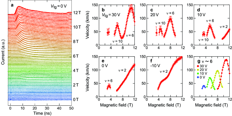
Figure 3 shows results for the sample with a top gate, which demonstrate that the plasmon velocity can be further changed by the gate. The behavior of the current pulse for the top gate bias V (Fig. 3a) is largely different from that for the ungated sample. Typical time of flight is 10 ns, which is one order of magnitude larger than that in the ungated sample. In the QH state for T, the time of flight increases with decreasing . Around T, weak signal for the QH state appears. The amplitude of the current pulse is small for away from QH states. Similar measurements for V were carried out, and the velocity is plotted in Figs. 3b-f. For V, the velocity oscillates around 100 km/s with peaks at and 6.2 T, where the and 10 QH states are formed, respectively. As is decreased, the field position of the peaks shifts to lower following the and, at the same time, the peak velocity decreases (Fig. 3g).
The smaller velocity is due to the screening of the electric field in plasmons by the gate. The degree of the screening is evaluated by with the gate-graphene distance and the velocity is given by [24, 25]
| (2) |
Note that this model is developed for a system without dissipation and valid only around QH states in our device. If we calculate using with , nm and nm, typical at becomes m. The unrealistically large is similar to the result for the ungated sample (Fig. 2d), again suggesting that the velocity of plasmons is reduced by interactions with their environment.
Meanwhile, the observed and dependence of the velocity cannot be explained by the dependence of ; rather, the oscillating behavior suggests a contribution of . Theory with the dissipation taken into account suggests that, in a gated two-dimensional electron system, the dissipation damps EMPs and, at the same time, slows EMPs down [25]. This is consistent with the oscillation of the velocity as a function of with peaks in QH states. The increase in the velocity at with suggests that the velocity increases with the gap of the QH state.
We demonstrated that plasmons propagate a distance of 1.1 mm with the velocity depending on , and the presence or absence of a gate. Quantitative analyses of the velocity suggested that interactions with dopants and dissipations slow plasmons down. This suggests that control of the environment of plasmons further increase the tunable range of the velocity. The wide-range tunability of the velocity and the observed large time of flight indicate that graphene is a promising material for plasmonics applications. Information on effects of and a gate is useful to design plasmonics devices.
Methods
We prepared a graphene wafer by thermal decomposition of a 4H-SiC(0001) substrate. SiC substrates were annealed at around 1,800 ∘C in Ar at a pressure of less than 100 Torr [22]. For the fabrication of devices, graphene and the SiC were mesa etched in a CF4/O2 atmosphere. After the etching, Cr/Au electrodes were deposited and then the surface was covered with 100-nm-thick HSQ and 40-nm-thick SiO2 insulating layers. For the injection gate and the top gate, Cr/Au was deposited on the insulating layers. Although steps of the SiC substrate have been reported not to affect the plasmon dispersion [26], to minimize this possible effect, the edge between the injection gate and the detector Ohmic contact is aligned parallel to the substrate steps.
References
- [1] Barnes, W. L., Dereux, A. & Ebbesen, T. W. Surface plasmon subwavelength optics. Nature 424, 824-830 (2003).
- [2] Maier, S. A. & Atwater, H. Plasmonics: localization and guiding of electromagnetic energy in metal/dielectric structures. J. Appl. Phys. 98, 011101 (2005).
- [3] Ozbay, E. Plasmonics: merging photonics and electronics at nanoscale dimensions. Science 311, 189193 (2006).
- [4] Ryzhii, V. Terahertz plasma waves in gated graphene heterostructures. Jp. J. Appl. phys. 45, L923-L925 (2006).
- [5] Rana, F. Graphene terahertz plasmon oscillators. IEEE Trans. NanoTechnol. 7, 91-99 (2008).
- [6] Jablan, M., Buljan, H. & Sljai, M. Plasmonics in graphene at infrared frequencies. Phys. Rev. B 80, 245435 (2009).
- [7] Mishchenko, E. G., Shytov, A. V. & Silverstrov, P. G. Guided plasmons in graphene p-n junctions. Phys. Rev. Lett. 104, 156806 (2010).
- [8] Ju, L. et al. Graphene plasmonics for tunable terahertz metamaterials Nature Nanotech. 6, 630 (2011).
- [9] Hwang, H. E. & Das Sarma, S. Dielectric function, screening, and plasmons in two-dimensional graphene. Phys. Rev. B 75, 205418 (2007).
- [10] Volkov, V. A. & Mikhailov, S. A. Edge magnetoplasmons: low-frequency weakly damped excitations in inhomogeneous two-dimensional electron systems. Zh. Eksp. Theor. Fiz. 94, 217-241 (1988) [Sov. Phys. JETP 67, 1639-1653 (1988)].
- [11] Aleiner, I. L. & Glazman, L. I. Novel edge excitations of two-dimensional electron liquid in a magnetic field. Phys. Rev. Lett. 72, 2935-2938 (1994).
- [12] Ashoori, R. C., Stormer, H. L., Pfeiffer, L. N., Baldwin, K. W. & West, K. Edge magnetoplasmons in the time domain. Phys. Rev. B 45, 3894-3897 (1992).
- [13] Zhitenev, N. B., Haug, R. J., Klitzing, K. v. & Eberl, K. Experimental determination of the dispersion of edge magnetoplasmons confined in edge channels. Phys. Rev. B 49, 7809-7812 (1994).
- [14] Kumada, N., Kamata, H. & Fujisawa, T. Edge magnetoplasmon transport in gated and ungated quantum Hall systems. Phys. Rev. B 84, 045314 (2011).
- [15] Bostwick, A., Ohta, T., Seyller, T., Horn, K. & Rotenberg, E. Quasiparticle dynamics in graphene. Nat. Phys. 3, 36-40 (2007).
- [16] Bostwick, A. et al. Observation of plasmarons in quasi-freestanding doped graphene. Science 328, 999-1002 (2010).
- [17] Plolini, M. et al. Plasmons and the spectral function of graphene. Phys. Rev. B 77, 081411 (2008).
- [18] Liu, Yu & Willis, R. F. Plasmon-phonon strongly coupled mode in epitaxial graphene. Phys. Rev. B 81, 081406 (2010).
- [19] Hwang, H. E., Sensarma, R. & Das Sarma, S. Plasmon-phonon coupling in graphene. Phys. Rev. B 82, 195406 (2010).
- [20] Jablan, M., Sljai, M. & Buljan, H. Unconventional plasmon-phonon coupling in graphene. Phys. Rev. B 83, 161409 (2011).
- [21] Williams, J. R., Low, T., Lundstrom, M. S. & Marcus, C. M. Gate-controlled guiding of electrons in graphene. Nature Nanotech. 6, 222 (2011).
- [22] Tanabe, S., Sekine, Y., Kageshima, H., Nagase, M. & Hibino, H. Half-integer quantum Hall effect in gate-controlled epitaxial graphene devices. Appl. Phys. Express 3, 075102 (2010).
- [23] The wide QH state is due to charge transfer between graphene and the donor state in SiC and/or in the insulating layer: Janssen, T. J. B. M. et al., Phys. Rev. B 83, 233402 (2011), K. Takase et al., to be submitted.
- [24] Zhitenev, N. B., Haug, R. J., Klitzing, K. v. & Eberl, K. Linear and nonlinear waves in edge channels. Phys. Rev. B 52, 11277-11283 (1995).
- [25] Johnson, M. D. & Vignale, G. Dynamics of dissipative quantum Hall edges. Phys. Rev. B 67, 205332 (2003).
- [26] Langer, T., Baringhaus, J., Pfnr, H., Schumacher, H. W. & Tegenkamp, C. Plasmon damping below the Landau regime: the role of defects in epitaxial graphene New J. Phys. 12, 033017 (2010).
Acknowledgement
The authors are grateful to K. Takase and K. Sasaki for fruitful discussions and to M. Ueki for experimental support. This work was supported in part by Grant-in-Aid for Scientific Research (21000004) and (21246006) from MEXT of Japan.
Author Contributions
N. K. performed experiments, analyzed data and wrote the manuscript. S. T. and H. H. grew the wafer. N. K, H. K., M. H., K. M., and T. F. discussed the results. All authors commented on the manuscript.