Fermi level tuning and a large activation gap achieved in the topological insulator Bi2Te2Se by Sn doping
Abstract
We report the effect of Sn doping on the transport properties of the topological insulator Bi2Te2Se studied in a series of Bi2-xSnxTe2Se crystals with 0 0.02. The undoped stoichiometric compound ( = 0) shows an -type metallic behavior with its Fermi level pinned to the conduction band. In the doped compound, it is found that Sn acts as an acceptor and leads to a downshift of the Fermi level. For 0.004, the Fermi level is lowered into the bulk forbidden gap and the crystals present a resistivity considerably larger than 1 cm at low temperatures. In those crystals, the high-temperature transport properties are essentially governed by thermally-activated carriers whose activation energy is 95–125 meV, which probably signifies the formation of a Sn-related impurity band. In addition, the surface conductance directly obtained from the Shubnikov-de Haas oscillations indicates that a surface-dominated transport can be achieved in samples with several m thickness.
pacs:
73.25.+i, 74.62.Dh, 72.20.My, 73.20.AtI Introduction
In a three-dimensional (3D) topological insulator (TI), a band inversion due to strong spin-orbit coupling induces gapless surface states (SS) consisting of spin helical Dirac Fermions,K1 ; MB ; Roy ; K2 ; Qi which are expected to give rise to a number of topological quantum phenomena. Kane ; ZhangSC Whereas such surface sensitive probes as angle-resolved photoemission spectroscopy (ARPES) and scanning tunneling microscope have been successfully applied to investigate the topological SS,ARPESHsieh ; ARPESmatsuda ; ARPESshen ; ARPESSato ; ARPESKuroda ; ARPESShen2 ; ARPESBTS ; ARPESBSTS ; STM1 ; STM2 ; STM3 ; STM4 the transport study of the SS remains a challenge due to the presence of parallel bulk conducting channel that usually dominates the transport properties.Taskin ; Ong2010 ; Fisher_np ; HorBi2Se3 ; checkelsky ; Butch ; Analytis ; Eto ; RenBi2Se3 Recently, the ternary tetradymite Bi2Te2Se (BTS) has become a prototype TI material for studying the peculiar spin and charge transport of the SS,RenBTS ; OngBTS because carefully prepared BTS crystals not only present a very low bulk conduction, but also show clear Shubnikov-de Haas (SdH) oscillations that reflect a high mobility of surface Dirac electrons. Given the lack of a truly bulk-insulating state in any of the known TI materials so far,RenBSTS ; BSTStaskin ; HgTe further improvement of BTS is worth pursuing.
The first synthesis of BTS was made while optimizing the continuous solid solutions between Bi2Te3 and Bi2Se3 for thermoelectric applications.Bi2Te3-xSex Nevertheless, unlike other members in the Bi2Te3-xSex (03) family, the Te and Se atoms in BTS occupy distinct crystallographic sites, forming quintuple layers arranged in the sequential order Te-Bi-Se-Bi-Te along the axis.BSTSordering Such chalcogen ordering is believed to provide structural basis for reducing bulk carriers and achieving high surface mobility.RenBTS Unfortunately, similar to Bi2Se3, the BTS crystals grown from the stoichiometric melts show -type metallic conduction with the electron density of 1019 cm-3.JiaBTS When the chalcogen stoichiometry is altered in the starting composition, one obtainsRenBTS ; JiaBTS metallic or insulating crystals at different positions along the boule, which is due to the inevitable phase separation during the solidification process, according to a newly established phase diagram of the Bi2Te3–Bi2Se3 system.BTScrystal Therefore, it is desirable to explore an alternative route to obtain BTS crystals with a large bulk resistivity while keeping the chalcogen stoichiometry, which would be useful for achieving a high surface-carrier mobility.
In this paper, we show that the above objective can be accomplished by hole doping through a Bi-site substitution, which has already been proven to be effective in tuning the carrier type and density for both of the binary end members, Bi2Te3 and Bi2Se3.ARPESshen ; Fisher_np ; HorBi2Se3 ; RenBi2Se3 It is found that, in analogy to its role in Bi2Te3,ARPESshen ; HeavilySnBTS ; SnBTS-Kulbachiskii ; SnBTS-resonant the group IV element Sn acts as an acceptor in BTS, which allows us to tune the Fermi level () of this material. In particular, the Bi2-xSnxTe2Se crystals with 0.004 show low-temperature resistivity reaching several cm, indicating that is tuned into the bulk band gap; their transport properties at high temperatures signify a large activation gap, which probably comes from a Sn-related impurity band. In about a half of those samples, we observed SdH oscillations originating from the topological surface state below 14 T. Our analysis of the SdH oscillations gives direct evidence that one can achieve a surface-dominated transport in a bulk Sn-doped BTS crystal with a thickness of several m.
II Experimental Details
The single crystals of Bi2-xSnxTe2Se were grown by melting high purity elemental shots of Bi (99.9999%), Sn (99.99%), Te (99.9999%), and Se (99.999%) with a nominal ratio of Bi:Sn:Te:Se = (2-)::2:1 ( = 0, 0.002, 0.004, 0.006, 0.01, 0.02) in sealed evacuated quartz tubes at 850 ∘C for 48 h with periodically shaking to ensure homogeneity, followed by cooling slowly to 500 ∘C and then annealing at that temperature for 4 days. The resulting crystals are easily cleaved along the (111) plane, revealing a shiny mirrorlike surface. The x-ray diffraction (XRD) analysis, which was performed on powders obtained by crushing the crystals, confirmed the samples to be single phase with chalcogen-ordered tetradymite structure.
For transport characterizations, the crystals were cut into bar-shaped samples with the typical thickness of 100 m after they were checked to be single domain by x-ray Laue analysis. The electrical leads were attached to the samples using room-temperature-cured silver paste in a six-probe configuration. The in-plane resistivity and the Hall coefficient were measured in a Quantum Design Physical Properties Measurement System (PPMS-9) down to 1.8 K. The magnetic field was applied along the axis which is perpendicular to the cleaved surface. For each value, the data were taken on several crystals obtained from different parts of the boule in order to check for sample-to-sample variation. In addition, selected samples were cleaved down to a few micrometers by using Kapton tapes and then brought to a 14-T magnet for the detection of SdH oscillations using an ac measurement technique, in which two lock-in amplifiers were employed to collect the signals in both the longitudinal () and transverse () channels simultaneously. The measurements were carried out by sweeping the magnetic field between 14 T at the rate of 0.3 T/min, during which the temperature was stabilized to within 5 mK.
III Results
III.1 Resistivity
Figure 1(a) shows typical data for the temperature dependences of in Bi2-xSnxTe2Se crystals with different values, together with the data for an insulating sample grown from the starting composition Bi2Te1.95Se1.05 which we abbreviate as BTS1.05. The undoped stoichiometric BTS crystal ( = 0) shows a metallic behavior in the whole temperature range; correspondingly, the Hall coefficient [inset of Fig. 2(a)] is negative and nearly temperature independent, giving an electron carrier density of 1.51019 cm-3 at 1.8 K. This result is in agreement with the previous study,JiaBTS which indicated that is pinned to the conduction band for this composition. Upon doping with Sn, a drastic change in both the resistivity value and its temperature dependence was observed. It is worth noting that an insulating behavior of is already established even for 0.1% of Sn doping to the Bi site ( = 0.002). For 0.004, the values reach a few cm, which are usually larger than that achieved in BTS1.05.RenBTS
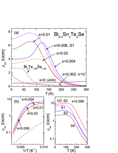
It should be noted that there is a marked difference in the () behavior between the Sn-doped BTS ( 0.004) and the BTS1.05 samples. Firstly, in the high-temperature region, in Sn-doped BTS samples increases more steeply with decreasing temperature, as can be seen more clearly in the Arrhenius plot shown in Fig. 1(b). The magnitude of at room temperature in Sn-doped BTS samples varies from 80 to 110 mcm, which are considerably larger than that in BTS1.05.RenBTS Also, the high-temperature slope in the Arrhenius plot, which is almost doping independent, corresponds to an activation gap of approximately 120 meV; this is nearly three times larger than that found for the BTS1.05 sample ( 45 meV). Secondly, in the low temperature region, while of the BTS1.05 sample becomes nearly flat, the Sn-doped BTS samples show a more strongly temperature-dependent behavior with a weak upturn below 10 K, whose origin is not clear at present.
In addition to the above observations, the Sn-doped BTS samples were found to show a higher degree of homogeneity. As an example, Fig. 1(c) shows the data for four samples obtained from different parts of a boule for = 0.006. One can see that all the samples show qualitatively similar temperature dependence of . Although the values still vary between samples by a factor of 4, it is notable that all of them are larger than 1 cm at low temperature.
III.2 Hall coefficient
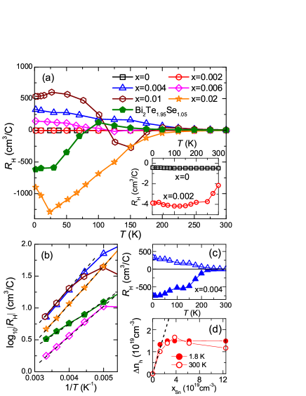
To further investigate the doping effect of Sn in BTS, we measured the Hall resistivity . Figure 2(a) shows the temperature dependences of the Hall coefficient for the same series of BTS1.05 and Bi2-xSnxTe2Se samples; here we follow our previous definition of as = near = 0.RenBSTS It turns out that 0.1% of Sn doping results in an increase in by nearly one order of magnitude, to cm3/C at 1.8 K [Fig. 2(a) inset]. Assuming a one-band model, this gives 1.61018 cm-3, implying that one Sn atom substituted for a Bi atom in BTS introduces approximately one hole, which is much the same as that in the case of -type Bi2Te3.ARPESshen While is negative for = 0 and 0.002 [Fig. 2(a) inset], it becomes positive at = 0.004 [Fig. 2(a) main panel], suggesting that an n-to-p type transition occurs as a result of Sn doping between = 0.002 and 0.004. In fact, in the case of = 0.004, both - and -type samples with a large were found in the same batch [Fig. 2(c)], placing this composition at the verge of such a transition. Somewhat unexpectedly, becomes negative again at a higher doping of = 0.02 [Fig. 2(a)], whose origin is not clear. In the following, we focus on the temperature dependence of for the samples with 0.004.
Above 200 K, of those samples shows a thermally activated behavior, indicating that is lowered into the bulk band gap. The effective activation gap , which is obtained from the Arrhenius plot of shown in Fig. 2(b), is 115, 95, 125, and 110 meV for the samples with = 0.004, 0.006, 0.01, 0.02, respectively. Actually, the values for all the measured crystals fall within 95–125 meV for those compositions. These values are not far from the values derived from the data, and their difference is likely due to the temperature dependence of the carrier mobility. More importantly, the values are much larger than that found in the BTS1.05 sample (65 meV), implying that the Sn doping brings closer to the middle of the band gap. At low temperatures, the values of those Sn-doped samples become large, sometimes exceeding 1000 cm3/C which would correspond to the carrier density of only 6 1015 cm-3 in a one-band model.
III.3 Surface quantum oscillations
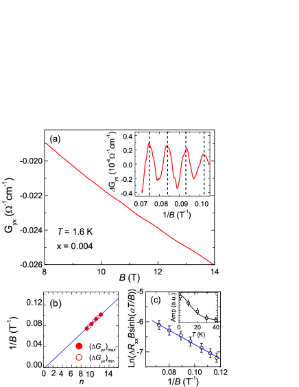
Although Sn doping is expected to introduce impurity scattering, it turned out that the surface mobility remains reasonably high so that SdH oscillations can still be observed. As a matter of fact, traces of SdH oscillations were detected in nearly 50% of the Sn-doped BTS samples measured in the 14-T magnet. Among those successful cases, the data taken on an -type sample with = 0.004 (thickness = 6 m) footnote showed the simplest pattern of the oscillations. In the following, we present the analysis of this simplest case.
Figure 3(a) shows the magnetic-field dependence of the transverse conductivity of this sample at 1.6 K, which was calculated from and . SdH oscillations are already visible in the raw data for magnetic field above 10 T. After removing a smooth background, one can clearly see that the oscillatory part of , , exhibits periodic maxima and minima as a function of [Fig. 3(a) inset], establishing the existence of a well defined Fermi surface (FS). In Fig. 3(b), we plot the values corresponding to the maxima (closed circles) and the minima (open circles) of as a function of the Landau level index , following the index assignment scheme in Ref. BTSberryphase, . From the linear fitting of the data with the slope fixed at the oscillation frequency obtained from the Fourier transform ( = 116 T), we obtain a finite intercept = 0.4 0.1. Since the slope is fixed in this analysis, the error in is relatively small; the main source of the error is the uncertainty in determining the positions of maxima and minima in the data shown in the inset of Fig. 3(a), and the error of 0.1 in is a conservative estimate. The obtained of 0.4 0.1 is reasonably close to the value = 0.5 expected for massless Dirac Fermions, which points to the topological SS origin of the SdH oscillations. Using the Onsager relation = (/2e), where is the extremal FS cross-section area, we find the Fermi wave vector = 5.9 106 cm-1, which corresponds to the surface carrier density = 2.8 1012 cm-2 for a spin-nondegenerate surface state. It is worth noting that if one assumes that the SdH oscillations originate from a bulk FS, the bulk carrier density implied by is of the order of 1018 cm-3, which is totally inconsistent with the large value observed at 1.8 K ( –100 cm3/C). Hence, one can conclude that the SdH oscillations are certainly coming from the surface. From the obtained value and the Fermi velocity 4.6 105 m/s,RenBTS is estimated to be 170 meV above the Dirac point, pointing to the electron character of the surface carriers.
By fitting the temperature dependence of the oscillation amplitude with the standard Lifshitz-Kosevich (LK) theory [inset of Fig. 3(c)], we obtained the cyclotron mass = 0.13, where is the free electron mass. Once is known, the Dingle plot [Fig. 3(c)] gives the Dingle temperature = 12.5 K, which corresponds to the surface quantum mobility of 1300 cm2/Vs. This value is roughly twice as large as that reported for thick BTS1.05 samples.RenBTS Surprisingly, according to these results, the ratio of the estimated surface conductance to the total conductance, given by , is calculated to be about 1.8 in this sample; here, the surface sheet conductance 5.8 10-4 , the measured overall conductivity was 0.64 cm-1 at 1.6 K, and = 6 m.note Obviously, it is unphysical to have 1, and this result implies that the actual surface transport is hindered by steps between terraces created upon cleaving, giving the effective surface conductance that is smaller than the intrinsic one given by and . Note that a similar problem was reported in Ref. BTSberryphase, . In any case, the SdH oscillations give direct estimate of the surface transport parameters, which indicate that a surface-dominated transport can be achieved in Sn-doped BTS crystals with several m thickness. The remaining bulk contribution is most likely the degenerate transport through the impurity band which is located in the bulk band gap; to further reduce the bulk contribution, one needs to achieve the Anderson localization in this impurity-band transport.
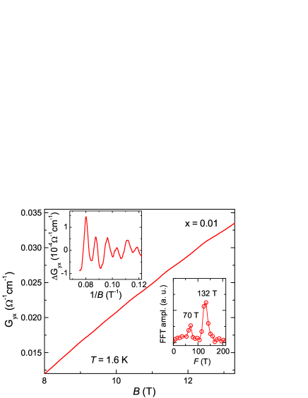
Apart from this simplest case, the patterns of the observed SdH oscillations were complicated. One of such examples, which was observed in a sample with = 0.01, is shown in Fig. 4. As can be seen in the lower inset, the Fourier transform of reveals two well-resolved peaks at = 70 T and = 132 T, reflecting the beating visible in the oscillation data (upper inset). The values calculated from the Onsager relation are 4.6 106 and 6.3 106 cm-1 for and , respectively. These correspond to of 1.7 1012 and 3.2 1012 cm-2, respectively. Unfortunately, as was pointed out in Ref. RenBi2Se3, , the multi-component nature of the oscillations prevents us from reliably extracting the cyclotron mass or the Dingle temperature for each component. Also, the Landau-level fan diagram is not very reliable for extracting in the multi-component case.
IV Discussions
From the above results, it is clear that Sn acts as an acceptor in BTS. Ideally, one would expect that the total number of holes introduced by Sn doping, , increases linearly with increasing . However, as can be seen in Fig. 2(d), becomes nearly constant for 0.004, which deviates significantly from the ideal situation. Therefore, there must be some additional effects that lead to deactivation of Sn dopants. In this respect, a similar problem was noted in previous studies of Sn doping in Bi2Te3, HeavilySnBTS ; SnBTS-Kulbachiskii ; SnBTS-resonant and two possibilities have been proposed to explain the apparent discrepancy.
One possibility considered for Bi2Te3 is that a part of the Sn atoms are built into the lattice in such a way that a seven-layer lamellar structure, Te-Bi-Te-Sn-Te-Bi-Te, is formed.HeavilySnBTS If a similar structure exists in Sn-doped BTS as well, it would be Se-Bi-Te-Sn-Te-Bi-Se. It is important to note that, in contrast to those occupying the Bi site, the Sn atoms in this structure do not bring any charge to the lattice, and thus the discrepancy is reconciled. However, no additional diffraction peaks except for those corresponding to the chalcogen-ordered tetradymite structure were observed in the XRD data even for the sample with the highest Sn-doping concentration (data not shown), suggesting that the seven-layer lamellae, if exist, are randomly distributed in the lattice.
Another, more plausible possibility is that, at high Sn-doping concentration, the wavefunctions of the Sn acceptors overlap significantly, leading to the formation of an impurity band (IB).SnBTS-Kulbachiskii ; SnBTS-resonant Within this picture, increasing Sn content results in an increase in the density of states (DOS) of the IB instead of hole doping. In Sn-doped Bi2Te3, this Sn-related IB was shown to be located at 15 meV below the top of the upper valence band.SnBTS-Kulbachiskii However, in the case of Sn-doped BTS, this Sn-related IB is most likely located within the bulk band gap, because the activation energy was found to be much larger in Sn-doped BTS than in BTS1.05, which naturally points to the appearance of a new IB to pin the chemical potential in Sn-doped BTS. Note that, while there may also be IBs due to Se vacancies and Bi/Te antisite defects in Sn-doped BTS, it is most likely that is pinned to the Sn-related IB due to its large DOS. The fact that the activation energy of 120 meV is essentially unchanged for a range of Sn concentrations ( = 0.004–0.02) is also consistent with this picture. Further studies are called for to clarify the details of the IBs in Sn-doped BTS.
V Conclusion
We performed a systematic study of the transport properties of a series of Bi2-xSnxTe2Se single crystals with 0 0.02. It is found that Sn behaves as an acceptor, which enables us to tune the Fermi level that is located in the conduction band in the undoped stoichiometric compound. For 0.004, is successfully tuned into the bulk band gap, and the resistivity becomes as large as several cm at low temperatures. The transport properties at high temperatures show a thermally activated behavior with a large activation gap, which is probably related to the formation of a Sn-related impurity band. The analysis of the SdH oscillations observed in a 6-m thick sample indicates that a surface-dominated transport can be achieved in Sn-doped BTS single crystals with several m thickness. This, along with the large activation gap, makes the Sn-doped BTS system well suited for future applications of topological insulators.
Acknowledgements.
This work was supported by JSPS (NEXT Program), MEXT (Innovative Area “Topological Quantum Phenomena” KAKENHI 22103004), and AFOSR (AOARD 104103 and 124038).References
- (1) L. Fu, C. L. Kane, and E. J. Mele, Phys. Rev. Lett. 98, 106803 (2007).
- (2) J.E. Moore and L. Balents, Phys. Rev. B 75, 121306(R) (2007).
- (3) R. Roy, Phys. Rev. B 79, 195322 (2009).
- (4) L. Fu and C.L. Kane, Phys. Rev. B 76, 045302 (2007).
- (5) X-L. Qi, T. L. Hughes, and S.-C. Zhang, Phys. Rev. B 78, 195424 (2008).
- (6) M.Z. Hasan and C.L. Kane, Rev. Mod. Phys. 82, 3045 (2010).
- (7) X.L. Qi and S.C. Zhang, Rev. Mod. Phys. 83, 1057 (2010).
- (8) D. Hsieh, D. Qian, L. Wray, Y. Xia, Y.S. Hor, R.J. Cava, and M.Z. Hasan, Nature 452, 970 (2008).
- (9) A. Nishide, A.A. Taskin, Y. Takeichi, T. Okuda, A. Kakizaki, T. Hirahara, K. Nakatsuji, F. Komori, Y. Ando, and I. Matsuda, Phys. Rev. B. 81, 041309(R) (2010).
- (10) Y.L. Chen, J.G. Analytis, J.-H. Chu, Z.K. Liu, S.-K. Mo, X.L. Qi, H.J. Zhang, D.H. Lu, X. Dai, Z. Fang, S.C. Zhang, I.R. Fisher, Z. Hussain, and Z.-X. Shen, Science 325, 178 (2009).
- (11) T. Sato, K. Segawa, H. Guo, K. Sugawara, S. Souma, T. Takahashi, and Y. Ando, Phys. Rev. Lett. 105, 136802 (2010).
- (12) K. Kuroda, M. Ye, A. Kimura, S.V. Eremeev, E.E. Krasovskii, E.V. Chulkov, Y. Ueda, K. Miyamoto, T. Okuda, K. Shimada, H. Namatame, and M. Taniguchi, Phys. Rev. Lett. 105, 146801 (2010).
- (13) Y.L. Chen, Z.K. Liu, J.G. Analytis, J.-H. Chu, H.J. Zhang, B.H. Yan, S.-K. Mo, R.G. Moore, D.H. Lu, I.R. Fisher, S.-C. Zhang, Z. Hussain, and Z.-X. Shen, Phys. Rev. Lett. 105, 266401 (2010).
- (14) S.Y. Xu, L.A. Wray, Y. Xia, R. Shankar, A. Petersen, A. Fedorov, H. Lin, A. Bansil, Y.S. Hor, D. Grauer, R.J. Cava, and M.Z. Hasan, arXiv:1007.5111v1.
- (15) T. Arakane, T. Sato, S. Souma, K. kosaka, K. Nakayama, M. Komatsu, T. Takahashi, Z. Ren, K. Segawa, and Y. Ando, Nat. Commun. 3, 636 (2012).
- (16) P. Roushan, J. Seo, C.V. Parker, Y.S. Hor, D. Hsieh, D. Qian, A. Richardella, M.Z. Hasan, R.J. Cava, and A. Yazdani, Nature 460, 1106 (2009).
- (17) Z. Alpichshev, J.G. Analytis, J.H. Chu, I.R. Fisher, Y.L. Chen, Z.X. Shen, A. Fang, and A. Kapitulnik, Phys. Rev. Lett. 104, 016401 (2010).
- (18) P. Cheng, C.L. Song, T. Zhang, Y.Y. Zhang, Y.L. Wang, J.F. Jia, J. Wang, Y.Y. Wang, B.F. Zhu, X. Chen, X.C. Ma, K. He, L.L. Wang, X. Dai, Z. Fang, X.C. Xie, X.L. Qi, C.X. Liu, S.C. Zhang, and Q.K. Xue, Phys. Rev. Lett. 105, 076801 (2010).
- (19) T. Hanaguri, K. Igarashi, M. Kawamura, H. Takagi, and T. Sasagawa, Phys. Rev. B 82, 081305(R) (2010).
- (20) A.A. Taskin and Y. Ando, Phys. Rev. B 80, 085303 (2009).
- (21) D.-X. Qu, Y.S. Hor, J. Xiong, R.J. Cava, and N.P. Ong, Science 329, 821 (2010).
- (22) J.G. Analytis, R.D. McDonald, S.C. Riggs, J.-H. Chu, G.S. Boebinger, and I.R. Fisher, Nat. Phys. 10, 960-964 (2010).
- (23) Y.S. Hor, A. Richardella, P. Roushan, Y. Xia, J.G. Checkelsky, A. Yazdani, M.Z. Hasan, N.P. Ong, and R.J. Cava, Phys. Rev. B 79, 195208 (2009).
- (24) J.G. Checkelsky, Y.S. Hor, M.-H. Liu, D.-X. Qu, R.J. Cava, and N.P. Ong, Phys. Rev. Lett. 103, 246601 (2009).
- (25) N.P. Butch, K. Kirshenbaum, P. Syers, A.B. Sushkov, G.S. Jenkins, H.D. Drew, and J. Paglione, Phys. Rev. B 81, 241301 (2010).
- (26) J.G. Analytis, J.H. Chu, Y. Chen, F. Corredor, R.D. McDonald, Z.X. Shen, and I.R. Fisher, Phys. Rev. B 81, 205407 (2010).
- (27) K. Eto, Z. Ren, A.A. Taskin, K. Segawa, and Y. Ando, Phys. Rev. B 81, 195309 (2010).
- (28) Z. Ren, A.A. Taskin, S. Sasaki, K. Segawa, and Y. Ando, Phys. Rev. B 84, 075316 (2011).
- (29) Z. Ren, A.A. Taskin, S. Sasaki, K. Segawa, and Y. Ando, Phys. Rev. B 82, 241306(R) (2010).
- (30) J. Xiong, A.C. Petersen, D.X. Qu, R.J. Cava, and N.P. Ong, arXiv:1101.1315.
- (31) Z. Ren, A.A. Taskin, S. Sasaki, K. Segawa, and Y. Ando, Phys. Rev. B 84, 165311 (2011).
- (32) A.A. Taskin, Z. Ren, S. Sasaki, K. Segawa, and Y. Ando, Phys. Rev. Lett. 107, 016801 (2011).
- (33) C. Brune, C. X. Liu, E. G. Novik, E. M. Hankiewicz, H. Buhmann, Y. L. Chen, X. L. Qi, Z. X. Shen, S. C. Zhang, and L. W. Molenkamp, Phys. Rev. Lett. 106, 126803 (2011).
- (34) N. Fuschillo, J.N. Bierly, and F.J. Donahoe, J. Phys. Chem. Solids 8, 430 (1959).
- (35) S. Nakajima, J. Phys. Chem. Solids 24, 479 (1963).
- (36) S. Jia, H.W. Ji, E. Climent-Pascual, M.K. Fuccillo, M.E. Charles, J. Xiong, N.P. Ong, and R.J. Cava, Phys. Rev. B 84, 235206 (2011).
- (37) O.B. Sokolov, S. Ya. Skipidarov, N.I. Duvankov, and G.G. Shabunina, J. Cryst. Growth 262, 442 (2004).
- (38) J. Horák, P. Lošťák, and J. Guerts, Phys. Stat. Sol. (b) 167, 459 (1991).
- (39) V.A. Kulbachinskii, M. Inoue, M. Sasaki, H. Negishi, W.X. Gao, K. Takase, Y. Giman, P. Lostak, and J. Horak, Phys. Rev. B 50, 16921 (1994).
- (40) C.M. Jaworski, V. Kulbachinskii, and J.P. Heremans, Phys. Rev. B 80, 233201 (2009).
- (41) In Bi1.5Sb0.5Te1.7Se1.3 samples with the thickness of several m, we observed BSTStaskin that the low-temperature undergoes a sign change with time and that the SdH frequency accordingly shows a drastic change. However, for the present sample, only a slight time evolution in and the SdH frequency was observed.
- (42) J. Xiong, Y.K. Luo, Y.H. Koo, S. Jia, R.J. Cava, and N.P. Ong, arXiv:1111.6031.
- (43) It should be noted that in the present experiment, the bottom surface of the sample was glued to a Kapton tape, so the top and bottom surfaces were in different environments. This means that the surface chemical potentials (and hence the surface carrier densities) for the top and bottom surfaces were most likely different; nevertheless, only a single frequency was observed in the SdH oscillations, suggesting that only one surface was responsible for the oscillations. We therefore considered only one surface in this calculation of .