PbTe/PbSnTe heterostructures as analogs of topological insulators
Abstract
We investigate theoretically the PbTe/Pb1-xSnxTe heterostructure grown in [111] direction, specifically a quantum wall (potential step of width ) of PbTe embedded in Pb1-xSnxTe. For large enough to lead to band inversion, and for large , there are well-known gapless interface states associated with four valleys. We show that for nm the three pairs of states from oblique valleys strongly couple, and become gapped with a gap meV. On the other hand, the interface states from the [111] valley are essentially uncoupled, and they retain their helical character, remaining analogous to states at surfaces of thin layers of three-dimensional topological insulators. This opens up a possibility of studying the physics of two-dimensional helical Dirac fermions in heterostuctures of already widely studied IV-VI semicondcutors.
I Introduction.
A large attention has been recently devoted to topological insulators (TIs), materials in which the topology of the bulk bandstructure guarantees the existence of robust (against non-magnetic disorder) spin-nondegenerate (helical) edge/surface states.Hasan and Kane (2010); Qi and Zhang (2011) TIs are essentially a subclass of narrow gap semiconductors, since their bandgaps must be smaller than typical energy scale of relativistic corrections to the bandstructure ( eV). In fact, the first two-dimensional TI was realizedKonig et al. (2007) in a quantum well of HgTe/HgCdTe, i.e. a heterostructure based on well-known compound narrow-gap semiconductors. Helical edge modes have also been recently reported in a heterostructure of InAs/GaSb.Knez et al. (2011)
Part of interest in TIs stems from the fact that they represent a new topological phase of noninteracting electrons: the TI character of a material is its bulk property, nontrivially encoded in the wavefunctions of the occupied (valence band) states. However, it is the presence of the helical edge/surface states which leads to observable consequences. In three dimensional strong (weak) TIs they consist of an odd (even) number of spin-nondegenerate Dirac cones,Fu and Kane (2007) and many interesting effects were predicted to occur when these states become gapped due to a perturbation,Hasan and Kane (2010); Qi and Zhang (2011) e.g. due to proximity to a superconductor Fu and Kane (2008) or a ferromagnet.Qi et al. (2008); Essin et al. (2009) The superconducting proximity effect was predicted to lead to a creation of Majorana excitations at the surface of a TI,Fu and Kane (2008) while covering the surface with a magnetic insulator was predicted to lead to new magnetoelectric effects.Qi et al. (2008); Essin et al. (2009) By now many materials have been shown to be 3D TIs (see Ref. Hasan and Kane, 2010 and references therein), with Bi2Se3 Xia et al. (2009) and Bi2Te3 Chen et al. (2009) gathering the most attention due to the feature of having a single Dirac cone at the surface. Despite a recent progress in gating of thin layers of Bi2Se3, Checkelsky et al. (2011); Sacepe et al. (2011); Kim et al. (2012) it would be desirable to investigate the helical surface states in a well-known semiconductor system, for which the growth and nanostructure processing are already mastered. One such platform is strained bulk HgTe.Brüne et al. (2011) In this article we propose to focus on heterostuctures of compound semiconductors from the IV-VI lead chalcogenide family, (Pb,Sn)Te.Nim
The superlattices of PbTe/Pb1-xSnxTe (with ) were thoroughly characterized.Kriechbaum et al. (1984) Due to the huge dielectric constant of PbTe, mesoscopic structures of PbTe/PbEuTe exhibit very robust ballistic transport properties.Grabecki et al. (2005, 2006); Kolwas et al. (2011) Both Mn and Eu can be incorporated into PbTe, and exchange coupling between their spins and the band carriers was studied.Dietl et al. (1994) Furthermore, there exist heterostructures of PbTe and europium chalcogenidesKepa et al. (2003); Lechner et al. (2005) such as EuSe and EuTe, which are magnetic semiconductors with rich phase diagrams. Finally, a superconducting proximity effect has been recently shown to exist at In-PbTe junctions.Grabecki et al. (2010) All these features suggest that IV-VI based heterostructure, if it hosted gapless helical states, could be a good candidate for investigations of phenomena related to TIs.
When changing the Sn content in Pb1-xSnxTe alloy, band inversion between the topmost valence band and the lowest conduction band occurs at . In an unstrained sample this happens simultaneously at the four points at the edges of the Brillouin zone. Since the topological class of the bandstructure changes at the instances of local bandgap closing,Murakami and Kuga (2008) after an even number of local band inversions this class remains the same. In fact, both PbTe and PbSnTe are in a topologically trivial class,Fu and Kane (2007) although very recently it was arguedHsieh et al. (2012) that SnTe is a topological crystalline insulator,Fu (2011) i.e. that it supports an even number of surface states for specific surface orientations. However, we focus here on the mutual band inversion between PbTe and PbSnTe, which leads to existence of interfacial helical states, predicted theoretically 25 years ago.Volkov and Pankratov (1985); Korenman and Drew (1987); Agassi and Korenman (1988); Pankratov (1990)
Such an interface of PbTe and Pb1-xSnxTe , at which four Dirac cones appear, is analogous to a surface of a weak TI. Recent research on weak TIs suggests that these cones are in fact protected against time-reversal invariant perturbations as long as these are not periodic and commensurate with the lattice spacing,Ringel et al. (2011); Mong et al. (2012) a situation which is rather improbable at an epitaxial interface of two materials with the same lattice structure. It would however be even more interesting if one could obtain a single gapless helical state at an interface. As we show in this article, this can be brought by a confinement effect in a properly designed PbTe/Pb1-xSnxTe heterostructure grown in [111] direction. This happens due to an anisotropic energy structure near the four L points, which leads to a much stronger coupling of oblique valley states from opposite interfaces, compared to the [111] valley along the growth direction. Note that a similar coupling opens up a gap in a thin layer of a TI.Liu et al. (2010a); Linder et al. (2009); Lu et al. (2010); Shan et al. (2010) With a proper choice of strain, composition, and layer width, we obtain practically gapless helical states for [111] valley, with Dirac points located in the finite-width-induced gap in the remaining three valleys.
The paper is organized in the following way. In Section II we describe the Hamiltonian at L-point band extrema in PbSnTe, and we note its close relation to the Hamiltonian describing the states at the point in Bi2Se3-type materials. In Section III we review the properties of helical states existing at the PbTe/Pb1-xSnxTe interface, and we re-express some known resultsVolkov and Pankratov (1985); Pankratov (1990); Korenman and Drew (1987); Agassi and Korenman (1988) in a manner that shows their complete analogy with the surface states of TIs. Then, in Section IV we present the main results of the paper, the calculation of electronic structure of a finite-width PbTe/Pb1-xSnxTe heterostructure. There we present our prediction that in a properly designed heterostructure one can have a practically gapless single Dirac cone, with its Dirac point located in the gaps of the states from the other valleys. Finally, in Section V we discuss a few practical issues related to the experimental realization of the proposed heterostructure.
II The Hamiltonian.
The electronic states near the L-point extrema in Pb1-xSnxTe are described by Dimmock’s Hamiltonian.Nim ; Kriechbaum et al. (1984) Since we focus on heterostructures grown in [111] direction, we choose the axis parallel to [111]. The Hamiltonian in the basis of , ,, (where transform like but do not change sign under reflection) is then given by
| (1) |
where , and . For [111] valley is a matrix with on the diagonal. We stress that a realistic large ratio of is crucial for our considerations. For remaining oblique valleys we replace with , where is a transformation matrix between the coordinate systems associated with the oblique valley , with along the valley direction, and , with along the growth axis: .
We take eV, corresponding to the gap inversion at , and eV.Kriechbaum et al. (1984) For the remaining parameters we take eVÅ2, eVÅ2, eVÅ, and eVÅ, and we neglect their composition which is, if any, very weak in the considered regime of . Fitting of the Hamiltonian parameters to the results of Nuclear Magnetic ResonanceHewes et al. (1973) measurements in Pb1-xSnxTe with up to showed no changes in and parameters, while the dependence of and was inferred to be very weak. In other worksApp a constant was inferred for up to , while was seen to change by an amount which extrapolates to about % change for compared to PbTe. Experimental data on the ratio collected in Ref. He and Grassie, 1985 also suggests a very weak dependence of these parameters on Sn content up to .
The strain described by tensor is accounted for by , in which the two entries correspond to blocks. Note that gives strain-dependent corrections to and . The acoustic deformation potentials are taken again as composition-independent: eV, eV, eV, and eV.Kriechbaum et al. (1984) The lattice constants of PbTe (SnTe) are taken as Å ( Å).
The above Hamiltonian is written in a form which allows one to immediately see that after a basis reordering it becomes the same as the recently studied model Hamiltonian describing the states near the point in the Bi2Se3 family of materials.Liu et al. (2010b) There, the TI phase occursLiu et al. (2010b, a) when , i.e. when the conduction and valence bands at point become inverted. As mentioned before, in unstrained Pb1-xSnxTe the inversion occurs simultaneously at four L points, and the bulk phase remains topologically trivial.
III Helical nature of interface states.
We first analyze interface-bound states (IBS) localized at two decoupled heterointerfaces of a very wide PbTe/Pb1-xSnxTe heterostructure grown in [111] direction. We assume that for we have the values of and corresponding to PbTe, while for , and correspond to Pb0.54Sn0.46Te. From the point of view of band lineup, this structure is in fact a finite width potential step - a quantum wall (QWa) instead of a quantum well (QWe).
We use the effective mass approximation and replace by in Eq. (1). As long as the intervalley coupling (due to alloy disorder or atomic-scale interface reconstruction) can be neglected, the presence of mutual band inversion at the interfaces guarantees the existence of helical Dirac-like IBS.Volkov and Pankratov (1985); Pankratov (1990) The dispersion and the spin structure of IBS is insensitive to exact profile of the interface,Volkov and Pankratov (1985); Pankratov (1990) with only the dependence of wavefunctions being affected in the region of interdiffusion. For simplicity we assume an abrupt interface,Korenman and Drew (1987); Agassi and Korenman (1988); Dugaev and Petrov (1994) and use the boundary conditions of continuity of the wavefunction and its derivative (the latter only when we consider nonzero terms). Note that these boundary conditions are sufficient in the case when, as we assume, the Hamiltonian’s parameters such as , , and are the same for both compounds.
Since our numerical calculations show that for realistic parameters the terms are of minor quantitative importance, we present much simpler analytical results obtained by neglecting them. We also focus on results for [111] valley, which we label with superscript (with denoting the oblique-valley results). The energies of the IBS are , where and (in oblique valleys the dispersion is of course anisotropic in ). The eigenvectors are 4-spinors , with denoting the left () and the right () interfaces, multiplied by appropriate functions describing the exponential decay away from a given interface. The inverse decay lengths are given by
| (2) |
in the middle layer and outside, with . Let us note that in the oblique valley case acquire an imaginary part at finite - however, what is crucial is the fact that at , is given by Eq. (2) with replaced by .
The two-dimensional subspaces of IBS at the two interfaces are spanned by 4-spinors , for which the subscripts signify that their components correspond to well-defined spin states, although they remain linear combinations of different orbitals. Defining we can write them as: , . Using these basis states we can write the 4-spinor parts of the IBS solutions: , and , where .
The helical nature of these states can be seen by calculating the expectation values of spin operators: , , i.e. the spin vector is perpendicular to , pointing clockwise (anticlockwise) for negative (positive) energy branch. The pattern on the interface is reversed. More generally cos we can write an effective surface Hamiltonian in the basis:
| (3) |
with the Pauli matrices operating in the respective two-dimensional spaces. Let us remark that the spin pattern for states from the oblique valleys is more complicated, with nonzero out-of-plane polarization.
All these results show complete analogy with the surface states in TIs such as Bi2Se3.Liu et al. (2010b) The difference is the existence of four pairs of IBS, with the states from all the valleys coexisting at a given energy in the bulk gap, showing that the PbTe/Pb1-xSnxTe heterointerface is analogous to a surface of a weak TI.
IV The effect of finite Quantum Wall width.
We assume that the lattice mismatch between PbTe and Pb0.54Sn0.46Te is shared in ratio between the two materials (i.e. assuming a common lattice constant corresponding to content of Sn). This requires an engineering of strain distribution by, e.g., choice of a substrate. If we neglect the terms the calculation is fairly straightforward.Korenman and Drew (1987); Agassi and Korenman (1988); Dugaev and Petrov (1994) With the terms and for a general valley direction we have to resort to solving the problem numerically.
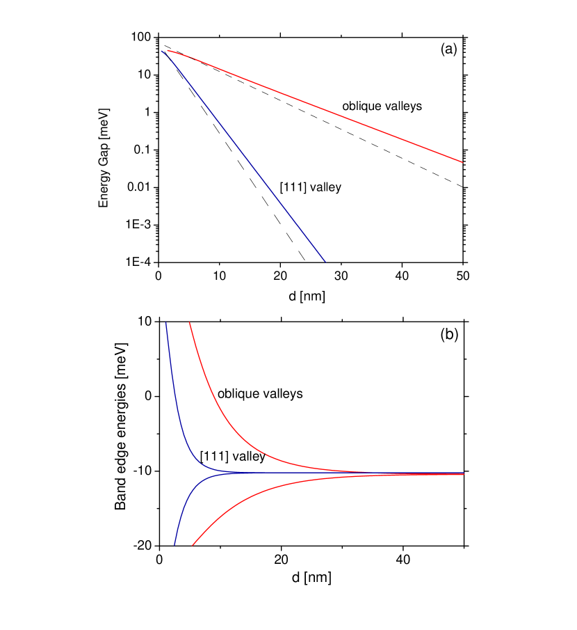
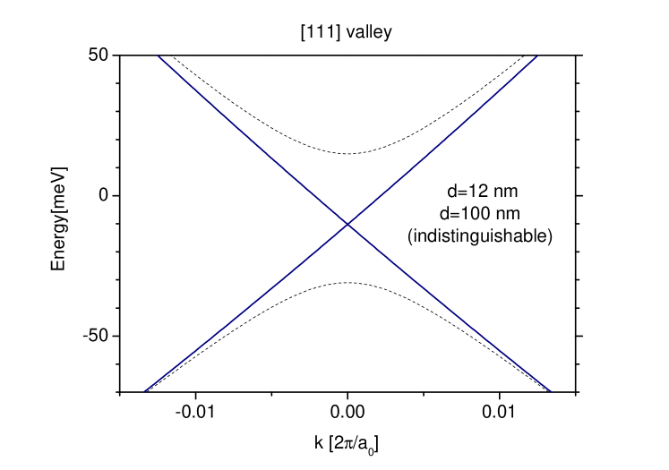
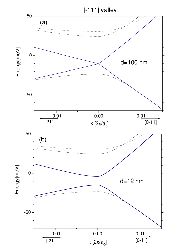
In Fig. 1 we show the energy dispersion of the [111] valley states formed in the QWa. For both widths of and nm the IBS from the two interfaces remain practically uncoupled: the gap opened for nm is only meV. On the other hand, as we show in Fig. 2, with decreasing a sizable gap opens for the interface bound (IB) derived states (formed due to the coupling of IBS from the opposite interfaces) in the oblique valleys, and it is meV for nm. As shown in Fig. 3a, the gaps are visibly different. Thus, for most of practical purposes (e.g. for experiments done at temperature K), in a structure with nm the dispersion of the states from the [111] valley can be considered gapless, while the states from the oblique valleys are gapped. Let us also stress that at energies , the eigenstates are essentially the L/R interface bound states (the description in terms of massive Dirac fermions Lu et al. (2010) is relevant only at small ). Furthermore, as shown in Fig. 3b, for the chosen QWa the [111] valley states are in the gap of the oblique valley solutions, so that disorder with typical energy scale smaller than this gap cannot mix the states from [111] valley with the others. Thus, for epitaxial interface of good quality we expect that the above-described system is basically equivalent to a layer of material such as Bi2Te3 or Bi2Se3, with the only difference being the smaller size of the gap within which the surface states exist ( meV vs eV).
The above results can be understood using a calculation with the terms neglected and assumed to be large. We orthogonalize the IBS and form their symmetric and antisymmetric combinations, approximating the exact solutions in large limit. We calculate the gap by evaluating the matrix elements of the QWa Hamiltonian between them. The -dependence of comes from exponential decay of the IBS in the step region, described by inverse lengths (calculated for ) given in Eq. (2) and below. In this way we obtain the bandgaps (see also Ref. Korenman and Drew, 1987)
| (4) |
The predictions of this formula agree well with the results of the full calculation shown in Fig. 3a.
V Discussion.
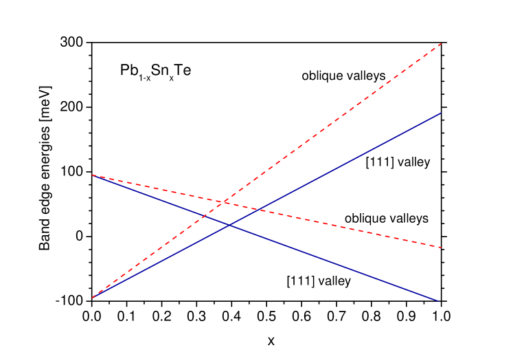
The above choice of a heterostructure was dictated by strain dependence of energies of band extrema in Pb1-xSnxTe. As shown in Fig. 4, when the lattice constant of Pb1-xSnxTe is adjusted to the PbTe constant in a heterostructure grown in [111] direction, with the realistic values of deformation potentials Kriechbaum et al. (1984) we obtain that the gaps at [111] L point and the remaining ones. One can see then that in the Pb1-xSnxTe quantum well (with PbTe being the barrier), it is practically impossible (without applying a compressive strain) to obtain a Dirac point of [111] valley IBS within the gap of the oblique valley IB-derived states. For the QWa with material parameters adopted here, we only require a modest amount of additional tensile strain, which could be provided at low temperatures by BaF2 substrate typically used for IV-VI compounds.Kriechbaum et al. (1984) Additional tuning of band edge offsets can also be obtained by using quanternary alloys and replacing a fraction of Te by Se.
Note however that if band-inverted Pb1-xSnxTe itself possesses gapless surface states,Hsieh et al. (2012) which would then appear at its interfaces with the substrate and with the gate covering the structure, then the choice of a compressively strained Pb1-xSnxTe /PbTe quantum well will be more experimentally practical. In such a case, apart from the IB-derived states we obtain also the “normal” quantum well states, with energies outside of the gap of Pb1-xSnxTe . The behavior of gaps of IB-derived states as a function of is analogous to the QWa case, and, provided that the appropriate compressive strain is aplied to the structure, the Dirac point of the [111] valley states can be located in the gap of the remaining IB-derived states (and, of course, also also in the gap of all the “normal” quantum well states).
Let us note that a result qualitatively the same as shown in Fig. 4 can be obtained for Pb1-xSnxTe uniaxially strained in [111] direction. The non-overlapping of bandgaps in the range of corresponding the inverted oblique valley and non-inverted [111] valley implies that applying such a strain, as proposed in Ref. Fu and Kane, 2007, cannot change Pb1-xSnxTe into a strong TI, but into a topological semimetal.
Another possible practical obstacle in investigation of helical states in the proposed structure is the issue of p-type self-dopingProkofievaa et al. (2010) of Pb1-xSnxTe with . This is analogous to the situation in materials from Bi2Se3 family, the members of which possess large bulk conductivity when as-grown, see e.g. Ref. Butch et al., 2010. At holes were compensated by indium doping,Khokhlov et al. (2000) but it remains to be investigated how effective this would be at considered here.
VI Conclusions.
We have calculated the bandstructure of a heterostructure based on PbTe and band-inverted Pb1-xSnxTe, in which PbTe forms a quantum wall (QWa) of finite thickness . The “normal” quantum well states are then absent, and the localized solutions appear due to the mutual band inversion between the constituent materials. For very large these solutions correspond to four pairs of Dirac cones located at the two interfaces.Volkov and Pankratov (1985); Korenman and Drew (1987); Agassi and Korenman (1988); Pankratov (1990) As the QWa grown in the [111] direction is narrowed, these states become gapped due to the overlap of wavefunctions localized on the two interfaces. We have found that the opened gap is at least two orders of magnitude larger for states associated with three oblique valleys compared to the states from the [111] valley. Thus, after properly choosing the QWa composition, its width, and the strain distribution in it, one can obtain a practically gapless pair of helical Dirac states from the [111] valley, with their Dirac point located in the gap of the states from the other valleys. The IV-VI heterostructure can then serve as an analogue of a thin layer of strong topological insulator.
VII Acknowledgements.
We thank T. Dietl, J. Tworzydło, G. Springholz, T. Story and G. Grabecki for discussions. We acknowledge support from Iuventus Plus grant (0060/H03/2010/70) of the Polish Ministry of Science, from EC network SemiSpinNet (PITN-GA-2008-215368), and from the EU FunDMS Advanced Grant of the European Research Council within the Ideas Seventh Framework Programme.
References
- Hasan and Kane (2010) M. Z. Hasan and C. L. Kane, Rev. Mod. Phys. 82, 3045 (2010).
- Qi and Zhang (2011) X.-L. Qi and S.-C. Zhang, Rev. Mod. Phys. 83, 1057 (2011).
- Konig et al. (2007) M. Konig, S. Wiedmann, C. Brune, A. Roth, H. Buhmann, L. W. Molenkamp, X.-L. Qi, and S.-C. Zhang, Science 318, 766 (2007).
- Knez et al. (2011) I. Knez, R.-R. Du, and G. Sullivan, Phys. Rev. Lett. 107, 136603 (2011).
- Fu and Kane (2007) L. Fu and C. L. Kane, Phys. Rev. B 76, 045302 (2007).
- Fu and Kane (2008) L. Fu and C. L. Kane, Phys. Rev. Lett. 100, 096407 (2008).
- Qi et al. (2008) X.-L. Qi, T. L. Hughes, and S.-C. Zhang, Phys. Rev. B 78, 195424 (2008).
- Essin et al. (2009) A. M. Essin, J. E. Moore, and D. Vanderbilt, Phys. Rev. Lett. 102, 146805 (2009).
- Xia et al. (2009) Y. Xia, D. Qian, D. Hsieh, L. Wray, A. Pal, H. Lin, A. Bansil, D. Grauer, Y. S. Hor, R. J. Cava, et al., Nat. Phys. 5, 398 (2009).
- Chen et al. (2009) Y. L. Chen, J. G. Analytis, J.-H. Chu, Z. K. Liu, S.-K. Mo, X. L. Qi, H. J. Zhang, D. H. Lu, X. Dai, Z. Fang, et al., Science 325, 178 (2009).
- Checkelsky et al. (2011) J. G. Checkelsky, Y. S. Hor, R. J. Cava, and N. P. Ong, Phys. Rev. Lett. 106, 196801 (2011).
- Sacepe et al. (2011) B. Sacepe, J. B. Oostinga, J. Li, A. Ubaldini, N. J. G. Couto, E. Giannini, and A. F. Morpurgo, Nat. Comm. 2, 575 (2011).
- Kim et al. (2012) D. Kim, S. Cho, N. P. Butch, P. Syers, K. Kirshenbaum, S. Adam, J. Paglione, and M. S. Fuhrer, Nat. Phys., advance online publication, DOI:10.1038/NPHYS2286 (2012).
- Brüne et al. (2011) C. Brüne, C. X. Liu, E. G. Novik, E. M. Hankiewicz, H. Buhmann, Y. L. Chen, X. L. Qi, Z. X. Shen, S. C. Zhang, and L. W. Molenkamp, Phys. Rev. Lett. 106, 126803 (2011).
- (15) G. Nimtz and B. Schlicht, in Narrow-Gap Semiconductors, Springer Tracts in Modern Physics Vol. 98, edited by G. Höhler (Springer-Verlag, Berlin, 1983), p. 1.
- Kriechbaum et al. (1984) M. Kriechbaum, K. E. Ambrosch, E. J. Fantner, H. Clemens, and G. Bauer, Phys. Rev. B 30, 3394 (1984).
- Grabecki et al. (2005) G. Grabecki, J. Wróbel, T. Dietl, E. Janik, M. Aleszkiewicz, E. Papis, E. Kamińska, A. Piotrowska, G. Springholz, and G. Bauer, Phys. Rev. B 72, 125332 (2005).
- Grabecki et al. (2006) G. Grabecki, J. Wróbel, T. Dietl, E. Janik, M. Aleszkiewicz, E. Papis, E. Kaminska, A. Piotrowska, G. Springholz, and G. Bauer, Physica E 34, 560 (2006).
- Kolwas et al. (2011) K. A. Kolwas, G. Grabecki, S. Trushkin, J. Wróbel, M. Aleszkiewicz, Ł. Cywiński, T. Dietl, G. Springholz, and G. Bauer, arXiv:1111.2433 (2011).
- Dietl et al. (1994) T. Dietl, C. Śliwa, G. Bauer, and H. Pascher, Phys. Rev. B 49, 2230 (1994).
- Kepa et al. (2003) H. Kepa, G. Springholz, T. M. Giebultowicz, K. I. Goldman, C. F. Majkrzak, P. Kacman, J. Blinowski, S. Holl, H. Krenn, and G. Bauer, Phys. Rev. B 68, 024419 (2003).
- Lechner et al. (2005) R. T. Lechner, G. Springholz, T. U. Schülli, J. Stangl, T. Schwarzl, and G. Bauer, Phys. Rev. Lett. 94, 157201 (2005).
- Grabecki et al. (2010) G. Grabecki, K. A. Kolwas, J. Wróbel, K. Kapcia, R. Puźniak, R. Jakieła, M. Aleszkiewicz, T. Dietl, G. Springholz, and G. Bauer, J. Appl. Phys. 108, 053714 (2010).
- Murakami and Kuga (2008) S. Murakami and S.-i. Kuga, Phys. Rev. B 78, 165313 (2008).
- Hsieh et al. (2012) T. H. Hsieh, H. Lin, J. Liu, W. Duan, A. Bansil, and L. Fu, arXiv:1202.1003 (2012).
- Fu (2011) L. Fu, Phys. Rev. Lett. 106, 106802 (2011).
- Volkov and Pankratov (1985) B. A. Volkov and O. A. Pankratov, JETP Lett. 42, 178 (1985).
- Korenman and Drew (1987) V. Korenman and H. D. Drew, Phys. Rev. B 35, 6446 (1987).
- Agassi and Korenman (1988) D. Agassi and V. Korenman, Phys. Rev. B 37, 10095 (1988).
- Pankratov (1990) O. A. Pankratov, Semicond. Sci. Technol. 5, S204 (1990).
- Ringel et al. (2011) Z. Ringel, Y. E. Kraus, and A. Stern, arXiv:1105.4351 (2011).
- Mong et al. (2012) R. S. K. Mong, J. H. Bardarson, and J. E. Moore, Phys. Rev. Lett. 108, 076804 (2012).
- Liu et al. (2010a) C.-X. Liu, H. Zhang, B. Yan, X.-L. Qi, T. Frauenheim, X. Dai, Z. Fang, and S.-C. Zhang, Phys. Rev. B 81, 041307 (2010a).
- Linder et al. (2009) J. Linder, T. Yokoyama, and A. Sudbø, Phys. Rev. B 80, 205401 (2009).
- Lu et al. (2010) H.-Z. Lu, W.-Y. Shan, W. Yao, Q. Niu, and S.-Q. Shen, Phys. Rev. B 81, 115407 (2010).
- Shan et al. (2010) W.-Y. Shan, H.-Z. Lu, and S.-Q. Shen, New J. Phys. 12, 043048 (2010).
- Hewes et al. (1973) C. R. Hewes, M. S. Adler, and S. D. Senturia, Phys. Rev. B 7, 5195 (1973).
- (38) G. Appold, R. Grisar, G. Bauer, H. Burkhard, R. Ebert, H. Pacher, H.G. H afele, Proc. 14th Int. Conf. Phys. Semicond. (ed. B.L.H. Wilson, Institute of Physics, Edinburgh 1979), p. 1101.
- He and Grassie (1985) Y. S. He and A. D. C. Grassie, J. Phys. F: Met. Phys. 15, 263 (1985).
- Liu et al. (2010b) C.-X. Liu, X.-L. Qi, H. Zhang, X. Dai, Z. Fang, and S.-C. Zhang, Phys. Rev. B 82, 045122 (2010b).
- Dugaev and Petrov (1994) V. K. Dugaev and P. P. Petrov, phys. stat. sol. (b) 184, 347 (1994).
- (42) Note that for , i.e. for , there is no real spin texture. What remains is the pseudospin texture described by Eq. (3), which still provides protection against elastic backscattering.
- Prokofievaa et al. (2010) L. V. Prokofievaa, Y. I. Ravich, D. A. Pshenay-Severin, P. P. Konstantinov, and A. A. Shabaldin, Semiconductors 44, 712 (2010).
- Butch et al. (2010) N. P. Butch, K. Kirshenbaum, P. Syers, A. B. Sushkov, G. S. Jenkins, H. D. Drew, and J. Paglione, Phys. Rev. B 81, 241301 (2010).
- Khokhlov et al. (2000) D. R. Khokhlov, I. I. Ivanchik, S. N. Raines, D. M. Watson, and J. L. Pipher, Appl. Phys. Lett. 76, 2835 (2000).