Magnetoresistance and negative differential resistance in NiGrapheneNi vertical heterostructures driven by finite bias voltage: A first-principles study
Abstract
Using the nonequilibrium Green function formalism combined with density functional theory, we study finite-bias quantum transport in NiGrNi vertical heterostructures where graphene layers are sandwiched between two semi-infinite Ni(111) electrodes. We find that recently predicted “pessimistic” magnetoresistance of 100% for junctions at zero bias voltage , persists up to V, which makes such devices promising for spin-torque-based device applications. In addition, for parallel orientations of the Ni magnetizations, the junction exhibits a pronounced negative differential resistance as the bias voltage is increased from V to V. We confirm that both of these nonequilibrium transport effects hold for different types of bonding of Gr on the Ni(111) surface while maintaining Bernal stacking between individual Gr layers.
pacs:
72.25.Mk, 73.43.Qt, 75.47.-m, 72.80.VpI Introduction
A magnetic tunnel junction (MTJ) consists of an ultrathin insulating barrier which separates two metallic ferromagnetic (F) layers with variable magnetization direction. The MTJs based on transition metals or their alloys and an epitaxial MgO barrier Butler2001 are the present workhorse of both commercial and basic research spintronics. For example, MgO-based MTJs are the core elements of read heads in hard drives or in magnetic random-access memory devices Katine2008 that are operated by the current-induced spin-transfer torque (STT). In the STT phenomenon, spin current of large enough density injected into a free F layer either switches its magnetization from one static configuration to another or generates a dynamical situation with steady-state precessing magnetization. Ralph2008 Thus, the usage of MTJs in STT-based spintronic devices necessitates Katine2008 ; Wang2011 a compromise between large current density (which requires low junction resistance to avoid damage) driven by finite bias voltage and readability (which requires large magnetoresistance).
One of the great successes of first-principles quantum transport modeling has been a conjecture Butler2001 of very large “optimistic” tunneling magnetoresistance, , in FeMgOFe(100) MTJs where () is conductance for parallel (antiparallel) orientation of the Fe magnetizations. This prediction has ignited intense fabrication efforts reaching TMR of about 200 % at room temperature Yuasa2004 which, although undoubtedly correlated with the crystallinity of MgO barrier, is difficult to reconcile with first-principles predictions. Butler2001 The origin of the discrepancy is the sensitivity of spin injection and TMR to details of difficult-to-control interfacial disorder as revealed by a number of theoretically investigated scenarios (such as the intermixing of Fe and MgO, Mathon2006 oxygen vacancies at or near the FeMgO interface, Ke2010 or substoichiometric FeO layers with small oxygen concentrations Bose2008 ). In addition, TMR in MgO-based MTJs decays precipitously Yuasa2004 ; Waldron2007 ; Rungger2009 with increasing bias voltage where the specific features of the decay are also sensitive to the type of interfacial disorder. Ke2010
These issues could be resolved by searching for new material systems which would ensure perfect spin filtering in the absence of disorder while being much less sensitive to the presence of interfacial disorder in realistic junctions. For example, the recent first-principles analysis Karpan2007 ; Karpan2008 has brought an example of such system—NiGrNi junctions—where layers of graphene (Grn) are sandwiched between two Ni electrodes as illustrated in Fig. 1. Graphene is recently discovered Castro-Neto2009 two-dimensional (2D) allotrope of carbon where electronic states of a single layer Gr1 or multilayers Grn close to the Fermi energy are located around the high symmetry point in reciprocal space. The NiGrNi junction exploits very small mismatch of % between the in-plane lattice constant of Gr and the surface lattice constant of Ni(111), as well as the fact that majority spin states of Ni are absent in a large region around the point. These two features combined lead to perfect spin filtering for , as quantified by the “pessimistic” magnetoresistance % (the “optimistic” MR diverges since vanishes for large ). The three times smaller lateral lattice mismatch compared to the 3.8% for conventional FeMgOFe junctions should also reduce some of the strain and amount of defects that otherwise limit the thickness and degrade the efficiency of spin injection in MgO-based MTJs.
However, very little is known about nonequilibrium transport driven by finite bias voltage in NiGrNi junctions. This is partly due to the fact that standard first-principles electronic transport tools employed to capture electronic and magnetic structure at interfaces, such as layer Korringa-Kohn-Rostoker approach applied Butler2001 to MgO-based MTJs or tight-binding muffin tin orbital wave-function matching scheme applied Karpan2007 ; Karpan2008 to NiGrNi junctions, become very cumbersome Zhang2004b to use at finite where one has to compute the charge redistribution Areshkin2010 due to current flow by evaluating the nonequilibrium density matrix —a procedure which ensures the gauge invariance Christen1996 of the current-voltage I-V characteristics. The nonequilibrium Green function formalism combined with density functional theory (NEGF-DFT), Areshkin2010 ; Taylor2001 ; Brandbyge2002 where DFT part of the calculations is implemented in the basis of local orbitals, makes it relatively straightforward to obtain .
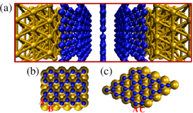
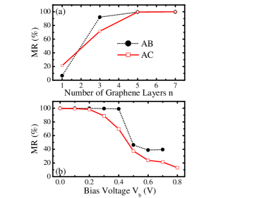
Here we show how to use efficiently spin- and -resolved NEGF-DFT framework to understand nonequilibrium transport through to NiGrNi junctions depicted in Fig. 1 for parallel (P) or antiparallel (AP) orientation of the Ni magnetizations. Our principal results are shown in Fig. 2 and Fig. 3. In Fig. 2(a), we first confirm the result of Ref. Karpan2007, ; Karpan2008, about the zero bias “pessimistic” MR reaching 100% for barriers composed of graphene layers and, moreover, in Fig. 2(b) we predict that such maximized MR would persist even at finite V. Figure 2(b) also suggests that bias voltage dependence of MR can be employed experimentally to determine the type of bonding configuration [illustrated in Figs. 1(b) and (c)] for Gr on the Ni(111) surface.
Furthermore, Fig. 3(c) shows that NiGrNi junction with P orientation of the Ni magnetizations will exhibit pronounced negative differential resistance (NDR), where total charge current first increases and then decreases as the bias voltage is increased from V to V (or symmetrically in the opposite direction). The origin of NDR is explained in Fig. 5 by plotting the position-dependent local density of states (LDOS) across the junction.
The paper is organized as follows. In Sec. II we discuss vertical NiGrNi heterostructure setup and how to tune the spin- and -resolved NEGF-DFT framework in order to describe properly magnetism around its interfaces. Section III discusses magnetoresistance at finite bias voltage, as well as the unusual conduction properties of general vertical graphene heterostructures, whose fabrication has been initiated recently, Lee2011 which make NiGrNi junctions different from either conventional MTJs or spin valves. In Sec. III, we discuss NDR in NiGrNi junctions driven by finite bias voltage. We conclude in Sec. V.
II The vertical heterostructure setup and tuning of NEGF-DFT framework for its modeling
The disorder-free junction shown in Fig. 1(a) consists of up to seven graphene layers arranged in Bernal stacking Castro-Neto2009 which serve as the barrier separating the two semi-infinite Ni electrodes. The junction is infinite in the transverse direction, so that its transverse periodicity requires -point sampling. Waldron2007 The spin injection and spin filtering in ferromagnetic multilayers depends not only on the properties of the F electrodes but also on geometry, bonding and electronic and magnetic structure of the contact region, as emphasized by the studies Butler2001 ; Waldron2007 of MgO-based MTJs. Therefore, we consider two different Gr on the Ni(111) surface bonding configurations illustrated in Figs. 1(b) and 1(c).
We note that DFT calculations employing different approximations for the exchange-correlation functional (such as local density approximation, Karpan2007 ; Karpan2008 generalized gradient approximation Fuentes-Cabrera2008 and van der Waals density functional Vanin2010 ; Mittendorfer2011 ) have yielded contradictory conclusions about the AC bonding configuration being the most stable energetically and the corresponding binding distance. The recent random phase approximation (RPA) calculations Olsen2011 have resolved this controversy and demonstrated the conflicting results are due to a delicate interplay between covalent and dispersive interactions which is not captured by the DFT functionals. Also, the scanning tunneling microscopy imaging Dedkov2010 shows that perfectly ordered epitaxial graphene layers can be prepared by elevated temperature decomposition of hydrocarbons where domains are larger than the terraces of the underlying Ni(111) surface.
The NEGF-DFT framework was originally developed Taylor2001 ; Brandbyge2002 to treat quantum transport through small molecules attached to metallic electrodes. Its application to modeling of charge and spin transport in MTJs requires careful tuning of pseudopotentials and basis sets in order to obtain an accurate description of the band structure near the Fermi level which is particularly important for the studies of spin-polarized transport. For example, pseudopotentials and localized basis sets that reproduce the electronic structure of the F electrode and barrier material alone do not necessarily reproduce the electronic structure of the more complicated F-electrodebarrier interfaces. Waldron2007
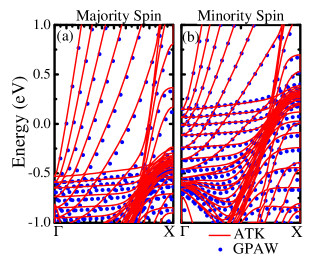
In order to capture accurately the electronic and magnetic structure around interfaces, we first compute the band structure of a periodic superlattice NiGrNiGr using DFT based on the projector augmented wave (PAW) methodology and wave function representation on uniform real-space grids as implemented in the GPAW code Enkovaara2010 where we choose grid spacing of Å. Within the PAW formalism one works implicitly with the all-electron wave functions and has access to the (frozen) core states which make the method applicable to a broad range of systems (including materials with strongly localized or electrons that can be problematic to describe with pseudopotentials). The same band structure is then recomputed using DFT where wavefunctions are represented in terms of the linear combination of atomic orbitals (LCAO) and the behavior of the core electrons is described by norm-conserving Troullier-Martins pseudopotentials, as implemented in the ATK code. quantumwise In the ATK-based calculations, we choose single -polarized (SZP) basis on C atoms and double -polarized (DZP) basis on Ni atoms. The Brioullin zone of the superlattice was sampled by -point grid, and the charge density and potentials were determined on a real-space grid with a mesh cutoff energy of 150 Ry. This was sufficient to achieve a total energy convergence of better than 0.01 meV/unit cell in the self-consistent loop.
The excellent agreement we achieve in Fig. 4 between the real-space grid PAW and LCAO pseudopotential DFT calculations, where Perdew-Burke-Ernzerhof (PBE) parameterization of the spin-polarized generalized gradient approximation (GGA) for exchange-correlation functional has been used in both cases, also selects the correct parameters to be used for LCAO pseudopotential part of NEGF-DFT analysis of two-terminal NiGrNi junctions discussed below. The active region of the device in Fig. 1(a) simulated by the NEGF-DFT code consists of 7 Ni(111) layers on the left, layers of Gr, and 6 layers of Ni(111) on the right. This active region is first relaxed until the maximum force component goes below per atom, and then attached to two semi-infinite ideal Ni electrodes.
The NEGF formalism for steady-state transport operates with two central quantities—the retarded and the lesser Green functions —which describe the density of available quantum states and how electrons occupy those states, respectively. In the NEGF-DFT framework, Areshkin2010 ; Taylor2001 ; Brandbyge2002 the Hamiltonian is not known in advance and has to be computed by finding the converged spatial profile of charge via the self-consistent DFT loop for the density matrix whose diagonal elements give charge density. Areshkin2010 The Hamiltonian matrix in the local orbital basis is composed of elements , where is the effective Kohn-Sham Hamiltonian obtained from the DFT self-consistent loop and the overlap matrix has elements .
In the coherent (i.e., in the absence of electron-phonon or electron-electron dephasing processes) transport regime, only the retarded Green function
| (1) |
of the active device region is required to post-process the result of the DFT loop by expressing the current between the left (L) and the right (R) electrodes
| (2) |
The electrodes are assumed to be attached to macroscopic reservoirs at infinity characterized by the Fermi function , so that bias voltage driving the nonequilibrium transport is given by . Here we resolve all quantities in minority and majority spin channels——assuming irrelevance of spin-orbit coupling or spin-flip scattering. The spin- and -resolved transmission function of coherent transport is given by
| (3) |
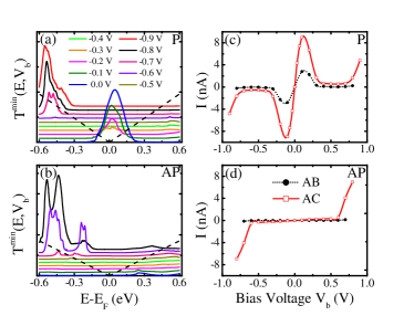
where the level broadening matrices are expressed in terms of the retarded self-energies of semi-infinite ideal Ni electrodes. In order to converge integration over the (conserved in the absence of disorder) transverse wavevector in Eq. (2), we find it necessary to use a dense grid of -points in the corresponding 2D BZ. This procedure yields the bias-dependent transmission function plotted in Figs. 3(a) and 3(b).
III Magnetoresistance at finite bias voltage
The NiGrNi multilayered heterostructure is not a conventional MTJ. Unlike MgO-based MTJs where linear-response () conductances and decay exponentially Butler2001 with increasing number of MgO layers, in the case of NiGrNi junction is independent of for (apart from an even-odd oscillation as a function of the thickness ). Karpan2007 ; Karpan2008 On the other hand, Grn acts as a tunnel barrier for majority spin electrons causing to decay exponentially with . The spin-resolved linear-response conductances for NiGrNi junctions are compared in 1 with the same conductances Butler2001 for FeMgOFe MTJ containing MgO barrier of similar thickness as our Gr5 barrier.
The recent first-principles analysis Kuroda2011 of different metalGrmetal junctions for , assuming reasonable metal-graphene epitaxial relationships, has delineated conditions for Grn to behave effectively as a tunnel barrier causing exponential decay of the conductance with increasing which requires crystal momentum mismatch between the bulk Fermi-level states in the metallic electrode and those in the Grn barrier. Furthermore, the recent experiments Lee2011 measuring I-V characteristics of metalGrmetal vertical junctions (with Ti/Pt used as top and bottom metal electrodes) has demonstrated application of the bias voltage up to V without encountering catastrophic breakdown while showing transitions from Ohmic (at very low bias) to power law () characteristics.
| NiGrNi(111) AC | |||
|---|---|---|---|
| NiGrNi(111) AB | |||
| FeMgOFe(100) |
In conventional MTJs, tunneling rates are higher if there are similar or identical states on both sides of the barrier. Therefore, the tunneling electrons need not only to get through the barrier but there must be a state of the correct symmetry on the other side to accept them. Butler2001 This effect is part of the reason for the commonly observed decrease in TMR with since as the bias increases the states on opposite sides of the barrier for P orientation differ more. Waldron2007 ; Rungger2009 ; Zhang2004b On the other hand, “pessimistic” MR in NiGrNi remains 100% up to V for Gr barrier of thickness , as shown in Fig. 2(b).
IV Negative differential resistance
Figures 3(c) and 3(d) plot the I-V characteristics for P and AP orientations of the Ni magnetizations where the total charge current is . Since in the AP orientation the bias-dependent transmission in Fig. 3(b) is nearly flat around the Fermi level, the I-V characteristics in Fig. 3(d) is linear up to the voltage V. However, in P orientation the total charge current sharply increases to reach its maximum value at V and then drops, thereby exhibiting a pronounced NDR. This feature can be explained using curves plotted for AC configuration in Fig. 3(a). At lower , the transmission resonance (around eV) falling into the bias window (marked by dashed wedge) contributes to the peak in the I-V characteristics. However, this resonance gets diminished with increasing which eventually shuts off the current flow when V is reached. The current is allowed to flow again when the new resonance around eV enters the bias window V.
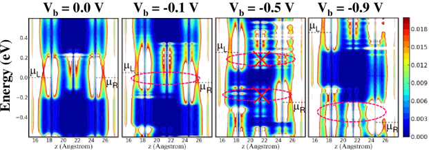
Further insight into the microscopic mechanism behind NDR in P orientation of magnetizations in NiGrNi junctions can be explained by examining the position-dependent LDOS
| (4) |
from the left to the right Ni electrode. The LDOS is plotted in Fig. 5 where we choose four bias voltage values ( V) at which the magnitude of the total charge current differs significantly. In equilibrium ( V), a prominent resonant state (white and red region) in the central Gr5 region is located close to the Fermi level and couples well with the conduction states on both sides of Ni electrode. Upon application of the bias voltage, both the position and the width of resonant states start to change. At V, part of the resonant state enclosed by the dotted oval still follows rigidly the upward-moving conduction state in the left Ni electrode while extending all the way to the downward moving conduction state in the right Ni electrode. As a result of this strong coupling between resonant conduction states within the energy interval enclosed by the electrochemical potentials of the two electrodes, the current increases notably. However, the charge density between the electrodes rapidly gets modified with the application of higher bias, and at V, the resonant state splits into two parts (at energies eV) thereby losing coupling to one of the Ni electrodes. Thus, almost no current flows at this bias voltage. Increasing further introduces a new state in the central region at energy eV which couples strongly to both Ni electrodes at V so that current starts increasing again.
V Concluding remarks
In conclusion, we demonstrated that perfect spin filtering in NiGrNi, with layers of graphene sandwiched between two (111) fcc Ni electrodes, characterized by “pessimistic” TMR=100% at zero bias voltage Karpan2007 ; Karpan2008 would persist even at finite bias voltage V. This feature is markedly different from conventional MgO-based MTJs where TMR drops sharply Waldron2007 ; Rungger2009 with increasing bias voltage. Thus, it could play an important role in spintronic devices based on STT. Katine2008 ; Wang2011 Furthermore, we predict that NiGrNi junction with P orientation of the Ni magnetizations would exhibit negative differential resistance as the bias voltage is increased from V to V due to transmission resonance formed at zero bias voltage which is then gradually pushed outside of the bias window.
Acknowledgements.
We thank K. S. Novoselov and J. Q. Xiao for illuminating discussions. This work was supported by DOE Grant No. DE-FG02-07ER46374 (K. K. S. and B. K. N.) and Danish National Research Foundation’s Center for Nanostructured Graphene (K. S. T.). The supercomputing time was provided in part by the NSF through XSEDE resource TACC Ranger under Grant No. TG-DMR100002 and NSF Grant No. CNS-0958512.References
- (1) W. H. Butler, X.-G. Zhang, T. C. Schulthess, and J. M. MacLaren, Phys. Rev. B 63, 054416 (2001).
- (2) J. Katine and E. E. Fullerton, J. Magn. Magn. Mater. 320, 1217 (2008).
- (3) D. Ralph and M. Stiles, J. Magn. Magn. Mater. 320, 1190 (2008).
- (4) C. Wang et al., Nature Phys. 7, 496 (2011).
- (5) S. Yuasa, T. N. A. F. Y. Suzuki, and K. Ando, Nature Mater. 3, 868 (2004).
- (6) J. Mathon and A. Umerski, Phys. Rev. B 74, 140404 (2006).
- (7) Y. Ke, K. Xia, and H. Guo, Phys. Rev. Lett. 105, 236801 (2010).
- (8) P. Bose, A. Ernst, I. Mertig, and J. Henk, Phys. Rev. B 78, 092403 (2008).
- (9) D. Waldron, L. Liu, and H. Guo, Nanotech. 18, 424026 (2007).
- (10) I. Rungger, O. Mryasov, and S. Sanvito, Phys. Rev. B 79, 094414 (2009).
- (11) V. M. Karpan et al., Phys. Rev. Lett. 99, 176602 (2007).
- (12) V. M. Karpan et al., Phys. Rev. B 78, 195419 (2008).
- (13) A. H. Castro Neto, F. Guinea, N. M. R. Peres, K. S. Novoselov, and A. K. Geim, Rev. Mod. Phys. 81, 109 (2009).
- (14) C. Zhang et al., Phys. Rev. B 69, 134406 (2004).
- (15) D. A. Areshkin and B. K. Nikolić, Phys. Rev. B 81, 155450 (2010).
- (16) T. Christen and M. Büttiker, Europhys. Lett. 35, 523 (1996).
- (17) J. Taylor, H. Guo, and J. Wang, Phys. Rev. B 63, 245407 (2001).
- (18) M. Brandbyge, J.-L. Mozos, P. Ordejón, J. Taylor, and K. Stokbro, Phys. Rev. B 65, 165401 (2002).
- (19) Y.-H. Lee, Y.-J. Kim, and J.-H. Lee, Appl. Phys. Lett. 98, 133112 (2011).
- (20) M. Fuentes-Cabrera, M. I. Baskes, A. V. Melechko, and M. L. Simpson, Phys. Rev. B 77, 035405 (2008).
- (21) M. Vanin et al., Phys. Rev. B 81, 081408 (2010).
- (22) F. Mittendorfer et al., Phys. Rev. B 84, 201401 (2011).
- (23) T. Olsen, J. Yan, J. J. Mortensen, and K. S. Thygesen, Phys. Rev. Lett. 107, 156401 (2011).
- (24) Y. S. Dedkov and M. Fonin, New J. Phys. 12, 125004 (2010).
- (25) J. Enkovaara et al., J. Phys.: Condens. Matter 22, 253202 (2010).
- (26) Atomistix ToolKit version 11.8, http://www.quantumwise.com
- (27) M. A. Kuroda, J. Tersoff, D. M. Newns, and G. J. Martyna, Nano Lett. 11, 3629 (2011).