Optical conductivity of Bismuth-based topological insulators
Abstract
The optical conductivity and the spectral weight of four topological insulators with increasing chemical compensation (Bi2Se3, Bi2-xCaxSe3, Bi2Se2Te, Bi2Te2Se) have been measured from 5 to 300 K and from sub-THz to visible frequencies. The effect of compensation is clearly observed in the infrared spectra, through the suppression of an extrinsic Drude term and the appearance of strong absorption peaks, that we assign to electronic transitions among localized states. From the far-infrared spectral weight of the most compensated sample (Bi2Te2Se) one can estimate a density of charge-carriers in the order of /cm3 in good agreement with transport data. Those results demonstrate that the low-energy electrodynamics in single crystals of topological insulators, even at the highest degree of compensation presently achieved, is still affected by extrinsic charge excitations.
pacs:
78.30.-j, 78.20.Ci,71.55.-i,73.25.+iTopological Insulators (TI) are new quantum materials with an insulating gap in the bulk, of spin-orbit origin, and metallic states at the surface Hasan1 ; Kane1 ; Moore1 . These states are chiral and show dissipation-less transport properties protected from disorder by the time-reversal symmetry. In addition to their fundamental properties, like exotic superconductivity Fu ; Nilsonn and axionic eletromagnetic response Qi ; Essin , TI have potential applications in quantum computing Fu1 ; Kitaev1 , THz detectors zangh and spintronic devices Chen . After the discovery of a topological behavior in three-dimensional (3D) BixSb1-x Hsieh , Bi2Se3 recently emerged, thanks to its large bulk insulating gap (300 meV), as the best candidate for the study of topological surface states Zhang . In fact, Dirac quasi-particles (DQP) related to the metallic surface states have been detected through Angle Resolved Photoemission Spectroscopy (ARPES) in Bi2Se3, Bi2Te3 and in their alloys Bi2Se2Te and Bi2Te2Se Xia ; Hsieh . Investigating the charge transport and cyclotron resonances of DQP has, however, proven to be challenging, because the surface current contribution is usually obscured by the extrinsic bulk carriers response [Qu, ; Basov, ; Butch, ].
Indeed, as-grown crystals of Bi2Se3 display a finite density of Se vacancies which act as electron donors. They pin the bulk chemical potential within the conduction band thus producing, over a wide range of carrier concentrations, extrinsic n-type degenerate semiconducting behavior. Se vacancies also affect the low-energy transport properties of those materials Cava1 , making it difficult to distinguish the intrinsic metallic behavior due to the topological surface state from the extrinsic metallic conduction induced by the Se non-stoichiometry. As a consequence, both transport and optical conductivity experiments Black ; Basov show a metallic behavior with a Drude term confined at low frequencies ( cm-1) which mirrors the extrinsic carrier content. Two phonon peaks interacting with the electronic continuum have been observed in the far-IR range near 61 cm-1 ( mode) and 133 cm-1 ( mode) Basov ; Richter . The bulk insulating gap instead spans between 250-350 meV, depending on the Se vacancy content, in good agreement with theoretical calculations Zhang1 . At variance with Bi2Se3, single crystals of Bi2Te3 display -type conductivity related to an excess of Bi atoms acting as acceptor centers Qu . These shift into the valence band so that, like for Bi2Se3, an extrinsic Drude term is observed in the far infrared (here below cm-1) Thomas .
Motivated by the above observations, different authors adopted specific strategies to reduce the non-stoichiometry-induced bulk carriers in Bi2Se3 (Bi2Te3) materials. Hor et al. showed that Ca-doping in the Bi site (Bi2-xCaxSe3) progressively shifts from the conduction band to the valence band, thus changing as-grown n-type Bi2Se3 into a p-type degenerate semiconductor Cava1 . By exploiting the different doping chemistry of Bi2Se3 (n-type) and Bi2Te3 (p-type), a better compensation was obtained in the Bi2Se2Te and Bi2Te2Se alloys Ando ; Cava2 . In both cases a variable range hopping (VRH) behavior and, at low-T, a high resistivity (exceeding 1 cm) were observed Ando ; Cava2 .
In this paper we present the first optical data of four topological insulators Bi2-xCaxSe3 ( = 0, 0.0002), Bi2Se2Te and Bi2Te2Se from 5 to 300 K and from the sub-THz to the visible spectral range. The effects of the enhanced compensation are clearly visible in the far-infrared (FIR) spectra, through the suppression of the Drude term and the appearance of strong absorption peaks that we assign to electronic transitions among localized states, similar to those found in weakly doped semiconductors. Our data show that the electrodynamics of Bi2Te2Se, i.e. the most compensated sample, is still affected by extrinsic doped charges, as therein the far-IR spectral weight is higher than the spectral weight associated with topological states by nearly two orders of magnitude.
Single crystals with = 0 were grown by a modified Bridgeman method, those of Bi2-xCaxSe3 via a process of two-step melting Cava1 . Chemical compensation ( the insulating character) increases when passing from Bi2Se3 and Bi2Se2Te to Bi2-xCaxSe3 and Bi2Te2Se Cava3 . The basal ()-plane resistivity of the most compensated sample, Bi2Te2Se, shows an increasing (semiconducting) behavior down to about 50 K followed by a low-T regime in which resistivity saturates at values exceeding 1 cm. In this regime, surface charge-carrier mobility much higher than the bulk mobility has been detected Cava2 ; Cava3 ; Jia .
The reflectivity of the four single crystals was measured at near-normal incidence with respect to the basal plane from sub-THz to visible frequencies at temperatures ranging from 5 to 300 K, shortly after cleaving the sample. The reference was obtained by in-situ evaporation of gold (silver) in the infrared (visible) range. In the sub-THz region (below 30 cm-1) we used Coherent Synchrotron Radiation (CSR) extracted from the electron storage ring BESSY II, working in the so-called low- mode AboBakr-03 . The real part of the optical conductivity was obtained from via Kramers-Kronig transformations, after extrapolating to zero frequency by Drude-Lorentz fits. The extrapolations to high frequency were based on data of Ref. Greenaway, .
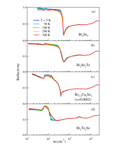
The reflectivity data for all samples are shown in Fig. 1. The far-infrared spectra in Figs. 1-a, -b are dominated by a free-carrier plasma edge around 500 cm-1 , which confirms the picture of an extrinsic electrodynamics in these materials. In Bi1.9998Ca0.0002Se3 (Fig. 1-c), Ca doping shifts the plasma edge to about 400 cm-1, while the strongest compensation is achieved in Bi2Te2Se (Fig. 1-d) where unshielded phonons are well resolved at 60 ( mode) and 130 ( mode) cm-1. In all spectra a strong electronic absorption appears above 10000 cm-1.
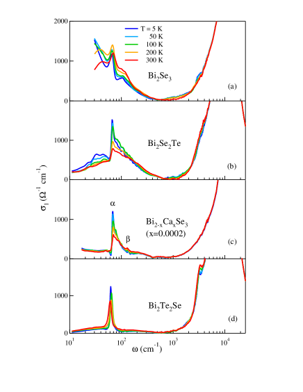
The real part of the optical conductivity obtained from the in Fig. 1 by Kramers-Kronig transformations is shown for the same temperatures and frequencies in Fig. 2. The direct gap transition, which corresponds to a small bump around 3000 cm-1 is barely visible due to its superposition with the huge triplet electronic excitation present above 10000 cm-1. These interband features, which will be not the focus of this paper, have been discussed in detail in Ref. Greenaway, . Most of the effects induced by compensation appears below 500 cm-1. In particular, the most extrinsic system Bi2Se3 (Fig. 2-a), presents a Drude term superimposed to the and phonon peaks, which both sharpen for decreasing T. A similar behavior has been observed by A. D. La Forge et al. in Ref. Basov, on crystal with a charge-carrier density in the same range 1018/cm3. The effect of compensation starts to be observable in Bi2Se2Te (Fig. 2-b). Here, at variance with an appreciable conductivity (200 cm-1 Cava4 ), most of the FIR spectral weight is located at finite frequency in the phonon spectral region. A further drastic reduction of the spectral weight is finally obtained in Bi1.9998Ca0.0002Se3 and Bi2SeTe2 (Figs. 2-c and -d).
The phonon mode, both in Bi2Se2Te and Bi1.9998Ca0.0002Se3, shows a Fano lineshape with a low frequency dip, more pronounced at low temperature. This suggests an interaction of this mode with an electronic continuum at lower frequency Damascelli . The Fano shape is much less evident in Bi2Te2Se, where the phonon shows a nearly Lorentzian shape at room and a weak low-frequency dip at low . This indicates that the electronic continuum SW transfers from above to below the phonon frequency for increasing temperature lupi_PRB98 . At variance with previous samples, the mode in Bi2Se3 shows instead a high-frequency dip at all T, confirming the observation in Ref. Basov, . This behavior is in agreement with an electronic-continuum SW located in average at higher frequency with respect the -phonon characteristic frequency.
In order to better follow the evolution of both the lattice and the electronic optical conductivity, we have fitted to a Drude-Lorentz (D-L) model where the phonon mode is described in terms of the Fano shape Damascelli . Examples of those fits (dotted lines) are shown in the insets of Fig. 3 at 5 K.
The FIR , as obtained after subtraction of both interband and phonon contributions, is shown in the same Figure. The electronic conductivity of Bi2Se3 (Fig. 3-a) can be described in terms of a Drude term (open circles) which narrows for decreasing in agreement with the metallic behavior of the resistivity Cava1 , and of a broad absorption centered around 150 cm-1 (open squares). In Bi2Se2Te (Fig. 3-b) most of the FIR spectral weight is located in a broad band centered around 100 cm-1. This band has been modelled through two Lorentzian contributions, located around 50 cm-1 (open triangles, FIR1) and 200 cm-1 (open squares, FIR2). In Bi1.9998Ca00002Se3 the increased compensation results in an overall reduction of the FIR spectral weight. Moreover, the FIR absorption already observed in Bi2Se2Te (Fig. 3-b) splits into two bands: a narrow absorption centered at about 50 cm-1 and a broader one around 200 cm-1. This double spectral structure is also achieved in Bi2Te2Se, where the low-frequency conductivity assumes a value comparable to the 1 cm-1 measured in crystals belonging to the same batch Cava2 .
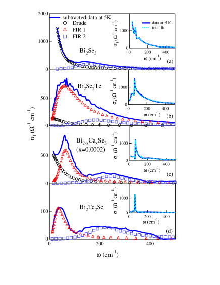
Similar low-frequency absorption bands in the optical conductivity have been observed in other, more conventional, doped semiconductors like Si:P Capizzi ; Gaymann . There, an insulator-to-metal transition (IMT) of Anderson type Mott , can be observed for a charge-carrier density 3.7 x 10¹⁸/cm3 Capizzi ; Gaymann . Deeply inside the insulating phase (), narrow peaks can be observed in the far-IR corresponding to the hydrogen-like transitions of isolated P impurities. They are followed by a broad band at higher frequency, due to the transitions from the impurity bound states to the continuum. The narrow peaks broaden for increasing doping, giving rise to a low-frequency band which however remains distinguished from the higher-frequency absorption. When approaching the IMT the low-frequency band transforms into a Drude term, while the high-frequency absorption persists in the metallic phase, indicating that the IMT occurs in an impurity band Gaymann . Therefore, in analogy with Si:P, the FIR2 band at 200 cm-1 in Bi1.9998Ca0.0002Se3 and Bi2Te2Se can be assigned to the transitions from the impurity bound states to the electronic continuum. The FIR2 band is also in very good agreement with the impurity ionization energy estimated from the T-dependence of resistivity and Hall data, namely 30-40 meV Cava2 ; Ando ; Bansal . Instead, the low-frequency FIR1 band, clearly resolved both in Bi1.9998Ca0.0002Se3 and Bi2Te2Se (Fig. 3-c and -d, respectively) can be associated with the hydrogen-like transitions, broadened by the inhomogeneous environment of the impurities and/or by their interactions. The spectra in Fig. 3 clearly show that, even in the most compensated topological insulator here measured, Bi2Te2Se, the far-IR conductivity is still affected by extrinsic charge-carriers injected into the system by non-stoichiometry and doping.
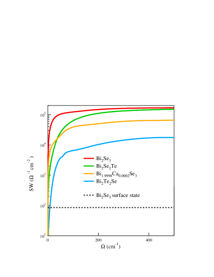
A more quantitative comparison between the charge density expected for the topological surface states and that provided by extrinsic charge carriers can be obtained by calculating the optical spectral weight :
| (1) |
where =500 cm-1, a cut-off frequency which well separates (see Fig.3), the low-frequency excitations from the interband transitions. In Fig. 4 one observes a decrease of one order of magnitude when passing from Bi2Se3 to Bi2Te2Se which confirms the drastic effect of chemical compensation. From the of Bi2Te2Se and assuming a carrier mass m Cava1 , one can estimate a 3D charge density /cm3. This value fits very well the interval 5 x 10¹⁶-2 x 10¹⁷/cm3 obtained from transport measurements in crystals of the same batch Jia .
Recently, the THz conductivity of Molecular Beam Epitaxy (MBE) Bi2Se3 films has been measured by a Time Domain Spectrometer from 200 GHz to about 2 THz Armitage1 ; Armitage2 . The optical conductivity in this spectral region, can be satisfactorily fits through a 2D Drude term plus the (3D) phonon mode. The 2D Drude contribution has been associated to topological surface states Armitage1 ; Armitage2 . Therefore their spectral-weight can be estimated from the plasma frequency () as obtained from the Drude fit in Refs. Armitage1, : . This value has been plotted in Fig. 4 through a dashed line. The actual in Bi2Te2Se is still nearly two orders of magnitude higher than that expected from the topological surface states. This result demonstrates that the low-energy electrodynamics in 3D single crystals of topological insulators, even at the highest degree of compensation presently achieved, is still affected by extrinsic charge excitations.
A further optimization in the crystal compensation is expected to provide crystals in which bulk techniques like infrared spectroscopy should be able to observe the intrinsic optical properties due to 2D surface metallic states.
We acknowledge the Helmholtz-Zentrum Berlin - Electron storage ring BESSY II for provision of synchrotron radiation at beamline IRIS. The research leading to these results has received funding from the European Community’s Seventh Framework Programme (FP7/2007-2013) under grant agreement n.226716. The crystal growth was supported by the US national Science Foundation, grant DMR-0819860.
References
- (1) M. Z. Hasan and C. L. Kane, Rev. Mod. Phys. 82, 3045 (2010).
- (2) C. L. Kane and E. J. Mele, Phys. Rev. Lett. 95, 226801 (2005).
- (3) J. E. Moore, Nature 464, 194 (2010).
- (4) L. Fu and C. L. Kane, Phys. Rev. Lett. 100 096407 (2008).
- (5) A. R. Akhmerov, J. Nilsson, and C.W.J. Beenakker, Phys. Rev. Lett. 102 216404 (2009).
- (6) X. -L. Qi, T.L. Hughes, and S.C. Zhang, Phys. Rev. B 78, 195424 (2008).
- (7) A. M. Essin, J.E. Moore, and D. Vanderbilt, Phys. Rev. Lett. 102 146805 (2009).
- (8) L. Fu and G. P. Collins, Sci. Am. 294, 57(2006).
- (9) A. Kitaev and J. Preskill Phys. Rev. Lett. 96, 110404 (2006).
- (10) X. Zhang, ,J. Wang, and S.C. Zhang, Phys. Rev. B 82, 245107 (2010).
- (11) Y. L. Chen, J. G. Analytis, J.-H. Chu, Z. K. Liu, S.-K. Mo, X. L. Qi, H. J. Zhang, D. H. Lu, X. Dai, Z. Fang, S. C. Zhang, I. R. Fisher, Z. Hussain, and Z.-X. Shen, Science 325, 178 (2009).
- (12) D. Hsieh, D. Qian, L. Wray, Y. Xia, Y. S. Hor, R. J. Cava, and M. Z. Hasan, Nature 452, 970 (2008).
- (13) H. Zhang, C. -X. Liu, X. -L. Qi, X. Dai, Z. Fang, and S.-C. Zhang, Nature Physics 5, 438 (2009).
- (14) Y. Xia, D. Qian, D. Hsieh, L. Wray, A. Pal, H. Lin, A. Bansil, D. Grauer, Y. S. Hor, R. J. Cava, and M. Z. Hasan, Nature Physics 5, 398 (2009).
- (15) Dong-Xia Qu, Y. S. Hor, Jun Xiong, R. J. Cava, and N. P. Ong, Science 329, 821 (2010).
- (16) A. D. La Forge, A. Frenzel, B. C. Pursley, Tao Lin, Xinfei Liu, Jing Shi, and D. N. Basov, Phys. Rev. B 81, 125120 (2010).
- (17) N. P. Butch, K. Kirshenbaum, P. Syers, A. B. Sushkov, G. S. Jenkins, H. D. Drew, and J. Paglione ,Phys. Rev. B 81, 241301 (2010) .
- (18) Y. S. Hor A. Richardella, P. Roushan, Y. Xia, J. G. Checkelsky, A. Yazdani, M. Z. Hasan, N. P. Ong, and R. J. Cava, Phys. Rev. B 79, 195208 (2009).
- (19) E. M. Black, E. M. Conwell, L. Seigle, C. W. spence Phys. Chem. Sol. 2, 240 (1957).
- (20) W. Richter, H. Kler, and C. R. Becker, Phys. Stat. Sol. (b) 84, 619 (1977).
- (21) H. Zhang, C. -X. Liu, X. -L. Qi, X. Dai, Z. Fang and S. -C. Zhang, Nat. Phys. 5, 438 (2009).
- (22) G. A. Thomas, D. H. Rapkine, R. B. Van Dover, L. F. Mattheiss, W. A. Sunder, L. F. Schneemeyer, and J. V. Waszczak , Phys. Rev. B 46, 1553 (1992).
- (23) Zhi Ren, A.A. Taskin, S. Sasaki, K. Segawa, and Y. Ando, Phys. Rev. B 82, 241306(R) (2010)
- (24) J. Xiong, Y. Luo, Y. Khoo, S. Jia, R. J. Cava, and N. P. Ong, Physica E: Low-dimensional Systems and Nanostructures 44 5 920 (2012).
- (25) J. Xiong, Y. Luo, Y. Khoo, S. Jia, R. J. Cava, and N. P. Ong, arXiv:1111.6031.
- (26) Shuang Jia Huiwen Ji, E. Climent-Pascual, M. K. Fuccillo, M. E. Charles, Jun Xiong, N. P. Ong, and R. J. Cava, Phys. Rev. B 84, 235206 (2011).
- (27) R. J. Cava private communication.
- (28) M. Abo-Bakr, J. Feikes, K. Holldack, P. Kuske, W. B. Peatman, U. Schade, and G. W?stefeld , Phys. Rev. Lett. 90, 094801 (2003).
- (29) D. L. Greenaway and G. Harbeke, J. Phys. Chem. Solids 26, 1585 (1965).
- (30) A. Damascelli, K. Schulte, D. van der Marel, and A.A. Menovsky, Phys. Rev. B 55, R4863 (1997).
- (31) S. Lupi, M. Capizzi, P. Calvani, B. Ruzicka, P. Maselli, P. Dore, and A. Paolone , Phys. Rev. B 57, 1248 (1998).
- (32) G.A. Thomas, M. Capizzi, F. DeRosa, R. N. Bhatt, and T. M. Rice Phys. Rev. B 23, 5472 (1981).
- (33) A. Gaymann, H.P. Geserich, and H.v. Lohneysen, Phys. Rev. B 52 16486 (1995).
- (34) N. F. Mott, Metal-Insulator transitions, Taylor and Francis, London (1990).
- (35) Y. S. Kim, M. Brahlek, N. Bansal, E. Edrey, G. A. Kapilevich, K. Iida, M. Tanimura, Y. Horibe, S. -W. Cheong, and S. Oh, Phys. Rev. B 84, 073109 (2011).
- (36) R. Valds Aguilar, A. V. Stier, W. Liu, L. S. Bilbro, D. K. George, N. Bansal, L. Wu, J. Cerne, A. G. Markelz, S. Oh, and N. P. Armitage, Phys. Rev. Lett. 108, 087403 (2012).
- (37) R. Valds Aguilar, L. Wu, A. V. Stier, L. S. Bilbro, M. Brahlek, N. Bansal, S. Oh, and N. P. Armitage arXiv:1202.1249.