Electrostatic doping of graphene through ultrathin hexagonal boron nitride films
The preparation of monolayers of graphite (graphene) has led to exciting discoveries associated with the unique electronic structure of this two-dimensional system.[1, 2] Transport experiments are usually performed in a field-effect device geometry with a graphene flake separated from a gate electrode by a dielectric spacer.[3, 4] Doped Si is commonly used as the gate material and SiO2 as the dielectric. Substrate inhomogeneities [5, 6] and trapped charges [7, 8] lead to local variations of the electrostatic potential at the SiO2 surface which results in uncontrolled local electron- and hole-doping of the graphene sheet, so-called electron-hole puddles.[9, 8]
With a layered graphene-like honeycomb structure and a lattice constant only 1.7% larger, insulating [10] h-BN would be the ideal substrate for graphene based devices;[11] the interaction between h-BN and graphene sheets is so weak that even if their lattices are forced to be commensurate, the characteristic electronic structure of graphene is barely altered. For an incommensurate stacking of graphene on h-BN, the perturbation is even smaller, leading to an extremely well-ordered graphene layer with a very high carrier mobility.[12, 13, 14]
Like graphene, h-BN layers can be prepared by mechanical exfoliation.[15] Cleaved layers can also be thinned to a single layer with a high-energy electron beam.[16] Alternatively, h-BN layers can be grown by chemical vapor deposition (CVD) on transition metals such as Cu or Ni, using precursors such as borazine (B3N3H6) or ammonia borane (NH3-BH3).[17, 18] With a proper choice of growth conditions, homogeneous ultrathin h-BN only 1-5 atomic layers thick can be grown. Moreover, graphene can be grown by CVD on top of a h-BN layer adsorbed on a metal substrate,[19] which is ideal for field-effect devices.
A field effect is created by applying a voltage difference between graphene and the metal substrate, resulting in charge accumulation or depletion in the graphene layer. We study this so-called electrostatic doping as a function of the thickness of the h-BN layer and the applied voltage using first-principles (DFT) calculations for a Cu(111)h-BNgraphene structure. In the absence of an applied voltage, a spontaneous charge transfer across the h-BN layer occurs between the metal substrate and the graphene, leading to an intrinsic doping of graphene. This transfer, which is driven by the difference in graphene and metal work functions, is strongly modified by the charge displacements resulting from the weak chemical interactions at the metalh-BN and at the h-BNgraphene interfaces.
By varying the applied voltage, the doping level can be controlled. Experimentally the position of the Fermi level in graphene has a square-root like dependence on the voltage.[20, 8, 21, 13, 14] We will demonstrate that this behavior is reproduced by our DFT calculations on Cu(111)h-BNgraphene and develop an analytical model that describes how the Fermi level depends on the applied voltage and the h-BN layer thickness.
Computational Details. We use DFT at the level of the local density approximation (LDA), within the framework of the plane-wave PAW pseudopotential method,[22] as implemented in VASP.[23, 24, 25] In our previous work we found that the LDA gives a reasonable description of the geometries resulting from the weak interactions between h-BN layers and between a h-BN and a graphene layer.[11] The change in the electronic structure of such systems in an external field is also described well.[26, 27, 28] The LDA also describes the interaction between graphene and metal (111) surfaces very reasonably.[29, 30, 31, 32, 33] We expect it to provide a description of the interaction between h-BN and metal (111) surfaces of similar quality. In contrast, we found that PW91 or PBE GGA functionals (incorrectly) predict essentially no interlayer binding between h-BN or graphene layers, or between metal (111) surfaces and h-BN or graphene sheets.
The Cu(111)h-BNgraphene structures are modeled in a supercell periodic in the direction with six Cu atomic layers in the (111) surface orientation, a slab 1-6 layers thick of h-BN, a graphene monolayer, and a vacuum region of Å. A dipole correction is applied to avoid spurious interactions between periodic images of the slab. We choose the lattice constant of graphene equal to its optimized LDA value Å, and scale the in-plane lattice constants of Cu(111) and h-BN so that the structure can be represented in a graphene surface unit cell.[11, 29, 30, 31] The positions of the atoms in graphene and h-BN, and of the top two atomic layers of the metal surface are allowed to relax during geometry optimization. The effect of the strain in the Cu and h-BN structures on the electronic structure is very small. For instance, the work function of Cu(111) is increased by a mere 0.04 eV and the density of states at the Fermi level is unaltered. An electric field applied across the slab is modeled with a sawtooth potential.[34]
In the most stable configuration of a h-BN monolayer on Cu(111), the nitrogen atoms are adsorbed on top of Cu(111) surface atoms and the boron atoms occupy hollow sites. The calculated equilibrium separation between h-BN and the Cu surface is 3.11 Å. The graphene and h-BN layers are stacked as in Ref. 11 with a calculated graphene-h-BN equilibrium separation of 3.21 Å, and a separation between h-BN layers of Å. The equilibrium structures are changed negligibly by the applied electric field, at least for field strengths up to V/Å. The interaction of graphene with h-BN is so weak that the characteristic linear band structure of graphene about the conical points is essentially preserved; a small band gap of meV is induced in graphene if the h-BN and the graphene lattices are commensurate. If they are incommensurate, the gap seems to disappear.[13, 12, 14] In the following this point will not be important.
Intrinsic Doping. We monitor the doping of graphene in the Cu(111)h-BNgraphene structure by calculating the change of the Fermi level with respect to neutral graphene. A computationally convenient way [30, 31] of characterizing is in terms of the difference between the work functions of the metaldielectricgraphene stack and for free-standing graphene,
| (1) |
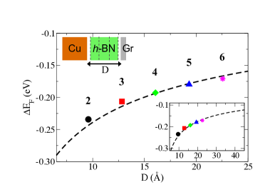
Negative (positive) values of then correspond to -type (-type) doping. Figure 1 shows as a function of the number of h-BN layers. These numbers are calculated without an external field which means that in the Cu(111)h-BNgraphene structure the graphene sheet is intrinsically doped with electrons. decreases with the number of h-BN layers. We will model this thickness dependence below.
The intrinsic doping originates from electrons that are transferred from the Cu electrode to the graphene sheet across the h-BN layer. However, the calculated work functions of Cu(111) and graphene are eV and eV, respectively. If charge transfer is driven by the difference between the Cu substrate and graphene work functions alone, then establishing a common Fermi level would require transferring electrons from graphene to Cu and the result would be -type doping, i.e. a positive value of , at variance with the results shown in figure 1. The h-BN layer must therefore play a non-trivial role.
The interaction between two materials at an interface generally results in the formation of an interface dipole. The latter can be visualized in terms of the electron rearrangement at the interface characterized by the electron density of the entire system minus the electron densities of the two separate materials (using identical, frozen atomic structures). As only the dependence perpendicular to the interface is relevant, it is convenient to work with plane-integrated electron densities where the integration is over the surface unit cell. The electron displacement in a Cu(111)h-BNgraphene stack is then described by . The result for a Cu(111)h-BNgraphene structure with five layers of h-BN is shown in figure 2.
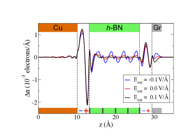
Dipoles are clearly visible at the interfaces between the different materials. The largest interface dipole is between Cu and h-BN. Electrons are piled up on the Cu surface implying depletion close to the h-BN surface. A similar effect is observed in the physisorption of organic molecules on metal surfaces,[35, 36] or even in the adsorption of noble gas atoms on metal surfaces.[37] There it is attributed to Pauli exchange repulsion between the adsorbate and the substrate, which results in a “push-back” of electrons towards the “softer” material, in this case the metal substrate.[37] This mechanism for interface dipole formation is quite general, and we speculate that the dipole at the Cu—h-BN interface has a similar origin. Between h-BN and graphene, one observes a similar but significantly smaller interface dipole. These dipoles are truly localized at the interfaces; their sizes do not depend on the number of h-BN layers as long as there is more than one. Both dipoles can also be obtained in separate calculations for the two interfaces, i.e. one for h-BN adsorbed on Cu(111), and one for graphene adsorbed on h-BN.
An interface dipole layer results in a discontinuity in the potential energy perpendicular to the interface. The potential energy step at an AB interface can be obtained from an AB slab calculation as the difference between the work functions on the A and the B sides of the slab. In practice, a single h-BN layer on top of the Cu(111) surface is sufficient to calculate the potential energy step at the Cu(111)h-BN interface. Similarly, the potential energy step at the h-BNgraphene interface can be determined with a system comprising two h-BN layers and the graphene sheet.
We find eV, and eV. Without additional charge transfer the difference between the Fermi levels in Cu and graphene in the Cu(111)h-BNgraphene structure would be
| (2) |
which we calculate to be eV. To achieve equilibrium requires transferring electrons between Cu and graphene to set up an electrostatic potential that compensates for . The sign of indicates that electrons are transferred from Cu to graphene, which results in -type doping, i.e. a negative value for , in agreement with figure 1.
External Field. The charge transfer leads to an intrinsic electric field across the h-BN slab, which polarizes the h-BN layers. This polarization is clearly identifiable in figure 2 as small oscillations of in the h-BN region in the absence of an external electric field (red line). It can be eliminated by applying an external electric field that opposes the intrinsic field. With V/Å the total internal electric field is zero, and the charge distribution in the h-BN slab becomes identical to that of a free-standing h-BN slab (black line). The blue line in figure 2 shows resulting from reversing the external field V/Å, that increases the polarization of the h-BN slab.
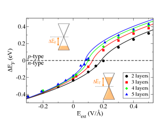
An external field can also be used to control the position of the Fermi level, i.e. the concentration of charge carriers, in graphene. [3, 4] Calculated Fermi level shifts for a range of h-BN slab thicknesses and external electric field values are plotted in figure 3. The curves for different h-BN slab thicknesses have a similar, highly nonlinear, shape. Similar shapes of the position of the Fermi level as a function of a gate voltage have been observed in scanning tunneling spectroscopy (STS) experiments,[20, 8, 13, 14] as well as in work function measurements.[21]
The points on the curves where correspond to the charge neutrality level of graphene, i.e. to undoped graphene. At these points the external field is equivalent to a potential difference across the h-BN slab that compensates for . We expect , where the thickness of the h-BN layer. The external field strength corresponding to the charge neutrality level should then decrease monotonically with increasing slab thickness, as is indeed observed in figure 3.
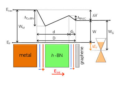
Model. To understand the intrinsic doping (fig. 1), as well as the external field effect (fig. 3) quantitatively, we develop the following analytical model whose parameters are shown in figure 4. The work function of the metaldielectricgraphene stack is given by , with the total potential difference across the stack. We model this potential difference as , where is the total electric field inside the dielectric, and is the elementary charge. This field can be related to an externally applied electric field by , with the dielectric constant of the dielectric layer and the surface charge density of the graphene sheet. These relations can be used in eq. 1 to derive a first expression for in terms of .
A second relation between and is obtained by noting that charge in graphene is introduced by (de)populating states away from the charge neutrality point, , and that the density of states near the conical points is well described by a linear function, , with /(eV2 unit cell)[30] and Å2 the area of a graphene unit cell. This then gives . Combining the two relations between and gives
| (3) |
where , is given by eq. 2, and eV/Å. The sign of is determined by the sign of . Equation 3 describes how the Fermi level in graphene depends on the gate voltage (or the external electric field ) and the thickness of the dielectric layer. We define as the separation between the top Cu layer and the graphene sheet minus a correction , because most of the displaced charge is localized between Cu and h-BN and between h-BN and graphene, see figure 2. We have used the value Å.[31] In principle the dielectric constant of the h-BN layer is a (weak) function of its thickness. We have used the constant value , which we calculate for a two-layer h-BN slab by putting the isolated slab in an external electric field[34]. We then determine the internal field by calculating the macroscopic average [38] of the electrostatic potential and differentiating it. The dielectric constant is then defined as the ratio between the internal and external field.
The results of this model are given in figures 1 and 3. The agreement with the results from the DFT calculations for the Cu(111)h-BNgraphene structures is very good. Note that the model has no adjustable parameters, as quantities such as (eq. 2) are obtained from separate calculations. The model correctly describes the intrinsic doping and its dependence on the h-BN layer thickness, fig. 1, as well as the dependence of the doping on the external field, fig. 3.
Summary. The doping of graphene in Cu(111)h-BNgraphene structures is studied by monitoring the Fermi level shift by means of first-principles DFT calculations. We predict that graphene is intrinsically -type doped for sufficiently thin h-BN layers. This is due to the potential difference between Cu and graphene arising from substantial dipole layers at the CuBN and the BNgraphene interfaces, as well as from the work function difference between Cu and graphene, eq. 2. The doping level decreases with increasing h-BN layer thickness, and approaches zero for thick layers. It can be varied by applying an external electric field and the resulting shift of the Fermi level has a modified square-root like dependence on the field. For thick dielectric spacers, and in the absence of work-function-difference and interface-dipole terms, this is similar to what is observed in experiments.[20, 8, 13, 14, 21] For very thin dielectric layers, these interface terms are predicted to play an important role and both the h-BN layer thickness dependence as well as the field dependence of the doping can be described quantitatively by an analytical model, eq. 3. The parameters of this model can be determined experimentally or obtained from DFT calculations on individual surfaces (the work functions of the metal and of graphene), on interfaces (the interface dipoles formed at the Cu(111)h-BN and the h-BNgraphene interfaces), or on slabs (the dielectric constant of a h-BN layer). Graphene field-effect devices using a thin layer h-BN gate dielectric should exhibit an intrinsic doping, and a dependence of the Fermi level on the applied gate voltage that is described by eq. 3.
Acknowledgement.We thank Thijs Veening for useful discussions. M.B. acknowledges support from the European project MINOTOR, grant no. FP7-NMP-228424. The use of supercomputer facilities was sponsored by the “Stichting Nationale Computerfaciliteiten (NCF)”, financially supported by the “Nederlandse Organisatie voor Wetenschappelijk Onderzoek (NWO)”.
References
- Novoselov et al. [2004] Novoselov, K. S.; Geim, A. K.; Morozov, S. V.; Jiang, D.; Zhang, Y.; Dubonos, S. V.; Grigorieva, I. V.; Firsov, A. A. Science 2004, 306, 666–669.
- Geim and Novoselov [2007] Geim, A. K.; Novoselov, K. S. Nature Materials 2007, 6, 183–191.
- Novoselov et al. [2005] Novoselov, K. S.; Geim, A. K.; Morozov, S. V.; Jiang, D.; Katsnelson, M. I.; Grigorieva, I. V.; Dubonos, S. V.; Firsov, A. A. Nature 2005, 438, 197–200.
- Zhang et al. [2005] Zhang, Y. B.; Tan, Y. W.; Stormer, H. L.; Kim, P. Nature 2005, 438, 201–204.
- Ishigami et al. [2007] Ishigami, M.; Chen, J. H.; Cullen, W. G.; Fuhrer, M. S.; Williams, E. D. Nano Letters 2007, 7, 1643–1648.
- Stolyarova et al. [2007] Stolyarova, E.; Rim, K. T.; Ryu, S.; Maultzsch, J.; Kim, P.; Brus, L. E.; Heinz, T. F.; Hybertsen, M. S.; Flynn, G. W. Proc. Natl. Acad. Sci. U.S.A. 2007, 104, 9209–9212.
- Chen et al. [2008] Chen, J.-H.; Jang, C.; Adam, S.; Fuhrer, M. S.; Williams, E. D.; Ishigami, M. Nature Physics 2008, 4, 377–381.
- Zhang et al. [2009] Zhang, Y. B.; Brar, V. W.; Girit, C.; Zettl, A.; Crommie, M. F. Nature Physics 2009, 5, 722–726.
- Martin et al. [2008] Martin, J.; Akerman, N.; Ulbricht, G.; Lohmann, T.; Smet, J. H.; Klitzing, K. V.; Yacoby, A. Nature Physics 2008, 4, 144–148.
- Watanabe et al. [2004] Watanabe, K.; Taniguchi, T.; Kanda, H. Nature Materials 2004, 3, 404–409.
- Giovannetti et al. [2007] Giovannetti, G.; Khomyakov, P. A.; Brocks, G.; Kelly, P. J.; van den Brink, J. Phys. Rev. B 2007, 76, 073103.
- Dean et al. [2010] Dean, C. R.; Young, A. F.; Meric, I.; Lee, C.; Wang, L.; Sorgenfrei, S.; Watanabe, K.; Taniguchi, T.; Kim, P.; Shepard, K. L.; Hone, J. Nature Nanotechnology 2010, 5, 722–726.
- Xue et al. [2011] Xue, J.; Sanchez-Yamagishi, J.; Bulmash, D.; Jacquod, P.; Deshpande, A.; Watanabe, K.; Taniguchi, T.; Jarillo-Herrero, P.; LeRoy, B. J. Nature Materials 2011, 10, 282–284.
- Decker et al. [2011] Decker, R.; Wang, Y.; Brar, V. W.; Regan, W.; Tsai, H.-Z.; Wu, Q.; Gannett, W.; Zettl, A.; Crommie, M. F. Nano Letters 2011, 11, 2291–2295.
- Novoselov et al. [2005] Novoselov, K. S.; Jiang, D.; Schedin, F.; Booth, T. J.; Khotkevich, V. V.; Morozov, S. V.; Geim, A. K. Proc. Natl. Acad. Sci. U.S.A. 2005, 102, 10451–10453.
- Meyer et al. [2009] Meyer, J. C.; Chuvilin, A.; Algara-Siller, G.; Biskupek, J.; Kaiser, U. Nano Letters 2009, 9, 2683–2689.
- Song et al. [2010] Song, L.; Ci, L.; Lu, H.; Sorokin, P. B.; Jin, C.; Ni, J.; Kvashnin, A. G.; Kvashnin, D. G.; Lou, J.; Yakobson, B. I.; Ajayan, P. M. Nano Letters 2010, 10, 3209–3215.
- Shi et al. [2010] Shi, Y.; Hamsen, C.; Jia, X.; Kim, K. K.; Reina, A.; Hofmann, M.; Hsu, A. L.; Zhang, K.; Li, H.; Juang, Z.-Y.; Dresselhaus, M. S.; Li, L.-J.; Kong, J. Nanoletters 2010, 10, 4134–4139.
- Usachov et al. [2010] Usachov, D.; Adamchuk, V. K.; Haberer, D.; Grueneis, A.; Sachdev, H.; Preobrajenski, A. B.; Laubschat, C.; Vyalikh, D. V. Phys. Rev. B 2010, 82, 075415.
- Zhang et al. [2008] Zhang, Y. B.; Brar, V. W.; Wang, F.; Girit, C.; Yayon, Y.; Panlasigui, M.; Zettl, A.; Crommie, M. F. Nature Physics 2008, 4, 627–630.
- Yu et al. [2009] Yu, Y. J.; Zhao, Y.; Ryu, S.; Brus, L. E.; Kim, K. S.; Kim, P. Nano Letters 2009, 9, 3430–3434.
- Blöchl [1994] Blöchl, P. E. Phys. Rev. B 1994, 50, 17953–17979.
- Kresse and Hafner [1993] Kresse, G.; Hafner, J. Phys. Rev. B 1993, 47, 558–561.
- Kresse and Furthmüller [1996] Kresse, G.; Furthmüller, J. Phys. Rev. B 1996, 54, 11169–11186.
- Kresse and Joubert [1999] Kresse, G.; Joubert, D. Phys. Rev. B 1999, 59, 1758–1775.
- Sławińska et al. [2010] Sławińska, J.; Zasada, I.; Klusek, Z. Phys. Rev. B 2010, 81, 155433.
- Sławińska et al. [2010] Sławińska, J.; Zasada, I.; Kosiński, P.; Klusek, Z. Phys. Rev. B 2010, 82, 085431.
- Ramasubramaniam et al. [2011] Ramasubramaniam, A.; Naveh, D.; Towe, E. Nano Letters 2011, 11, 1070–1075.
- Karpan et al. [2007] Karpan, V. M.; Giovannetti, G.; Khomyakov, P. A.; Talanana, M.; Starikov, A. A.; Zwierzycki, M.; van den Brink, J.; Brocks, G.; Kelly, P. J. Phys. Rev. Lett. 2007, 99, 176602.
- Giovannetti et al. [2008] Giovannetti, G.; Khomyakov, P. A.; Brocks, G.; Karpan, V. M.; van den Brink, J.; Kelly, P. J. Phys. Rev. Lett. 2008, 101, 026803.
- Khomyakov et al. [2009] Khomyakov, P. A.; Giovannetti, G.; Rusu, P. C.; Brocks, G.; van den Brink, J.; Kelly, P. J. Phys. Rev. B 2009, 79, 195425.
- Wintterlin and Bocquet [2009] Wintterlin, J.; Bocquet, M. L. Surface Science 2009, 603, 1841–1852.
- Feibelman [2008] Feibelman, P. J. Phys. Rev. B 2008, 77, 165419.
- Resta and Kunc [1986] Resta, R.; Kunc, K. Phys. Rev. B 1986, 34, 7146–7157.
- Rusu et al. [2009] Rusu, P. C.; Giovannetti, G.; Weijtens, C.; Coehoorn, R.; Brocks, G. J. Phys. Chem. C 2009, 113, 9974–9977.
- Rusu et al. [2010] Rusu, P. C.; Giovannetti, G.; Weijtens, C.; Coehoorn, R.; Brocks, G. Phys. Rev. B 2010, 81, 125403.
- Bagus et al. [2002] Bagus, P. S.; Staemmler, V.; Wöll, C. Phys. Rev. Lett. 2002, 89, 096104.
- Baldereschi et al. [1988] Baldereschi, A.; Baroni, S.; Resta, R. Phys. Rev. Lett. 1988, 61, 734–737.