Metallic Coulomb Blockade Thermometry down to 10 mK and below
Abstract
We present an improved nuclear refrigerator reaching 0.3 mK, aimed at microkelvin nanoelectronic experiments, and use it to investigate metallic Coulomb blockade thermometers (CBTs) with various resistances . The high- devices cool to slightly lower , consistent with better isolation from the noise environment, and exhibit electron-phonon cooling and a residual heat-leak of 40 aW. In contrast, the low- CBTs display cooling with a clearly weaker -dependence, deviating from the electron-phonon mechanism. The CBTs agree excellently with the refrigerator temperature above 20 mK and reach a minimum- of mK.
Advancing to ever lower temperatures can open the door for the discovery of new physics: for example, submillikelvin temperatures in quantum transport experiments could lead to novel nuclear-spin physicsSimon and Loss (2007); Simon et al. (2008) in nanoscale semiconductor devices Hanson et al. (2007) or could facilitate the study of non-Abelian anyons, Majorana Fermions and topological quantum computation in fractional quantum Hall samplesNayak et al. (2008); Stern (2010). However, cooling of nanoscale devices below mK is a formidable challenge due to poor thermal contact as well as microwave and other heating, often resulting in device and/or electron temperatures raised well above the refrigerator temperature. Therefore, significant progress beyond the status quo in both cooling techniques and thermometry is necessary.
One approach to overcome these difficulties uses Ag sintersLounasmaa (1974); Pobell (2007); Pickett (1988) to thermalize the sample wiresSamkharadze et al. (2011), pioneered by the Florida groupPan et al. (1999); Huang et al. (2007). Another approach – pursued by our Basel groupClark et al. (2010) – is to use nuclear coolingLounasmaa (1974); Pobell (2007); Pickett (1988) on the sample wires, with the potential to advance well into the microkelvin range. Thermometry in this regimeLounasmaa (1974); Pobell (2007); Pickett (1988) typically faces similar challenges as cooling nanostructures and is ideally integrated on-sample. Among numerous sensorsSpietz et al. (2006), Coulomb blockade thermometersPekola et al. (1994) (CBTs) are simple to use and self-calibrating yet offer high accuracy, demonstrated down to mKMeschke et al. (2010). Here, we present an improved nuclear refrigerator for cooling nanoelectronic samples and use it to investigate CBTs and their mechanisms of cooling.
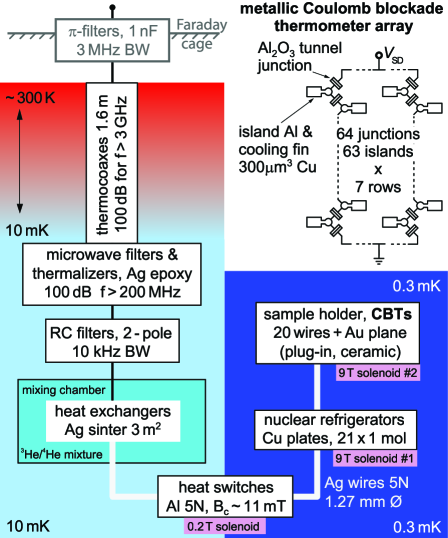
We employ a novel scheme for cooling electronic nanostructures into the microkelvin regime by thermalizing each sample wire directly to its own, separate nuclear refrigerator (NR) Clark et al. (2010). In this scheme, the sample cools efficiently through the highly conducting wires via electronic heat conduction, bypassing the phonon degree of freedom since it becomes inefficient for cooling at low . A prototype of this refrigerator presented in Ref. Clark et al., 2010 has been significantly improved in a 2nd generation system, briefly outlined below and in Fig. 1. A network of 21 parallel NRs is mounted on a rigid tripod intended to minimize vibrational heating. Two separate T magnets allow independent control of the NR and sample magnetic field.
Several stages of thermalization and filtering are provided on each sample wire (see Fig. 1). After -filters and thermocoaxZorin (1995), each lead passes through a Ag-epoxy microwave filter Scheller et al. , followed by an RC filter. Each wire then feeds into a Ag-sinter in the mixing chamber (MC), emerging as a massive high-conductivity Ag wire. After Al heat-switches with fused joints, each lead traverses a separate Cu NR via spot-welded contacts, terminating in an easily-exchangeable chip-holder plugged into Au-plated pins which are spot welded to the Ag wires. Therefore, excellent thermal contact () is provided between the bonding pads and the parallel network of 21 Cu pieces – the microkelvin bath and heart of the nuclear refrigerator – while maintaining electrical isolation of all wires from each other and from ground, as required for nanoelectronic measurements.
The performance of the NRs is evaluated in a series of demagnetization runs. The temperature of the Cu pieces is obtained using a standard techniquePobell (2007); Pickett (1988); Clark et al. (2010): after demagnetization, we apply power on heaters mounted on some of the NRs and evaluate the warm-up time-dependence measured with LCMN thermometers above mK. This allows us to determine both the temperature of the Cu-NRs after demagnetization as well as a small field-offset. For each demagnetization run, the NRs are precooled to mK in a T magnetic field and then demagnetized to temperatures as low as mK after the field has been slowly ramped down to T, giving efficiencies . Reruns showed excellent repeatability, allowing us to chart for various . To determine during the CBT experiments, we use the LCMN thermometers above mK, warm-up curves at the lowest and in-between, the pre-charted values.
The network with 21 NRs allows measurements of several CBTs (2-wire each). The CBT devices are Au-wire bonded and glued to the Au backplane of the chip carrier which is also cooled with a NR. Each CBT consists of 7 parallel rows of 64 Al/Al2O3 tunnel-junctions in series with an area of fabricated using e-beam lithography and shadow evaporation. The process used allows oxidation at elevated temperatures, giving junction resistances up to . Each island extends into a large cooling fin made from Cu, since Cu gives excellent electron-phonon coupling. A small mT is applied perpendicular to the sensor wafer to suppress the superconductivity of the Al. The differential conductance through a CBT sensor was measured with a standard lock-in technique adding a small ac excitation to a dc bias . Note that only of the applied voltage drops across each junction and the sensor resistance is times the junction resistance , assuming identical junctions.
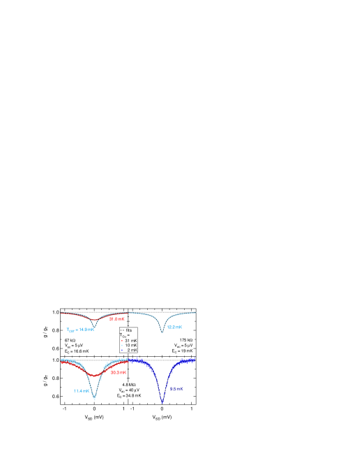
We investigated CBTs with various , see Fig. 2. Due to Coulomb blockade effects, the conductance around zero bias is suppressed below the large-bias conductance . Both width and depth of the conductance dip are related to the CBT electron temperature . To extract , we perform fits (dashed curves) using a numerical model from Ref. Meschke et al., 2004. We find excellent agreement between model and data (see Fig. 2). Independently, can be obtainedMeschke et al. (2004) from the conductance dip with and charging energy . We first extract at high- assuming and then use this to extract from everywhere. While both methods produce very similar (deviating slightly only at the lowest ), the approach makes no a-priori assumptions about the cooling mechanism, allowing us an unbiased investigation, though now requiring high- calibration against another thermometer (CMN). All values given here are from the method.
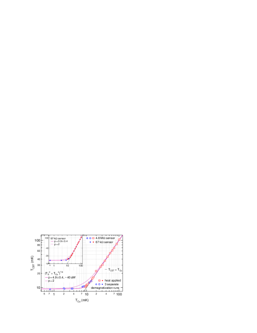
The thermalization properties of of the lowest and highest CBTs are displayed in Fig. 3 for a wide range of from mK to mK. As seen, excellent agreement is found between and at high temperatures, as expected. Further, is seen to lie well above at the lower temperatures (see Fig. 2 and 3), decoupling fully from well below mK. We note that was experimentally chosen to avoid self heating. Also, the sensor reaches lower temperatures than the other, lower impedance CBTs, consistent with better isolation from the environment, since the power dissipated is proportional to , with environmental noise voltage .
To model the CBT thermalizationMeschke et al. (2004), we write down the heat flow onto a single island with electron temperature :
| (1) |
where is a parasitic heat leak and is the voltage drop across the junction, appearing here in the Joule heating term. is the Cu electron-phonon (EP) coupling constant, the island volume and the phonon bath temperature assumed to be equal to . This is well justified by the high thermal conductance between the NRs and bonding pads. Note that at K, the sample-to-Au-backplane interface resistance (Kapitza) is small compared to the EP coupling resistance Meschke et al. (2004). Within this model, two cooling mechanisms are included: Wiedemann-Franz (WF, term) and EP cooling. Note the strong dependence of the EP term, ultimately rendering WF cooling dominant at sufficiently low . Assuming one mechanism and simplifying to only one island gives a saturation curve , with a CBT saturation temperature and an exponent , corresponding to for WF-electron cooling and for EP cooling.
We study the mechanism of thermalization by fitting the saturation curve first to the data. We find very good agreement, giving (see Fig. 3), indicating that EP coupling presents the dominant cooling mechanism, limiting to mK even though mK. Using , a small parasitic heat leak aW results for each island, with from Ref. Meschke et al., 2004. We speculate that could be caused by electrical noise heating such as microwave radiation, intrinsic residual heat release from materials used or other heat sources. Considering the high- junctions and correspondingly weak WF cooling, it is not surprising that EP coupling is dominant here.
When analogously examining the low- sensors, on the other hand, we find and mK for the sensor (see inset Fig. 3), and even and mK for a sensor (not shown) mounted on a conventional dilution refrigerator (base-mK) with improved filtering and chip-holder. Note that is the extrapolated saturation-. The lowest measured here was mK. These power-laws far below indicate that EP cooling is no longer dominant but, rather, a more efficient mechanism takes over at the lowest- in the low- sensors.
In summary, we have demonstrated operation of the NRs down to mK while the CBTs cool as low as mK. Though the high- sensor is obviously cooled by EP coupling, the low- sensors, interestingly, appear to be entering a different cooling regime. However, the low- sensors have slightly higher given the same environment, consistent with stronger coupling to the environment. The lowest CBT temperatures are limited by the parasitic heat leak, which is drained by the cooling channels available.
To further improve the sensor performance, the cooling-fin volume can be increased or the heat leak can be reduced, potentially using improvements in microwave shielding and filtering, e.g. using on-chip capacitors, metal planes or alternative array designs. Such efforts will strongly enhance thermalization if a more efficient cooling mechanism is indeed present, since otherwise, in the EP regime, reducing by 5 orders of magnitude will only reduce by a factor of ten.
An alternative avenue based on quantum dot CBTs, e.g. in GaAs, might also be rewarding, taking advantage of a much larger and level spacing . The resulting reduced sensitivity to the environment might allow a single dot to be used, rather than an array, cooling the reservoirs directly via the WF term, rather than through a long series of junctions.
Acknowledgements.
We would like to thank R. Blaauwgeers, G. Frossati, R. Haley, G. Pickett, V. Shvarts, P. Skyba and A. de Waard for very useful discussions. This work was supported by the Swiss Nanoscience Institute SNI, NCCR QSIT, Swiss NSF, ERC starting grant, and EU-FP7 SOLID and MICROKELVIN.References
- Simon and Loss (2007) P. Simon and D. Loss, Phys. Rev. Lett. 98, 156401 (2007).
- Simon et al. (2008) P. Simon, B. Braunecker, and D. Loss, Phys. Rev. B77, 045108 (2008).
- Hanson et al. (2007) R. Hanson, L. P. Kouwenhoven, J. R. Petta, S. Tarucha, and L. M. K. Vandersypen, Rev. Mod. Phys. 79, 1217 (2007).
- Nayak et al. (2008) C. Nayak, S. H. Simon, A. Stern, M. Freedman, and S. Das Sarma, Rev. Mod. Phys. 80, 1083 (2008).
- Stern (2010) A. Stern, Nature 464, 187 (2010).
- Lounasmaa (1974) O. V. Lounasmaa, Experimental Principles and Methods Below 1K (Academic, London, 1974).
- Pobell (2007) F. Pobell, Matter and Methods at Low Temperatures (Springer, Berlin, 2007).
- Pickett (1988) G. R. Pickett, Rep. Prog. Phys. 51, 1295 (1988).
- Samkharadze et al. (2011) N. Samkharadze, A. Kumar, M. J. Manfra, L. N. Pfeiffer, K. W. West, and G. A. Csáthy, Rev. Sci. Instr. 82, 053902 (2011).
- Pan et al. (1999) W. Pan, J.-S. Xia, V. Shvarts, D. E. Adams, H. L. Stormer, D. C. Tsui, L. N. Pfeiffer, K. W. Baldwin, and K. W. West, Phys. Rev. Lett. 83, 3530 (1999).
- Huang et al. (2007) J. Huang, J. S. Xia, D. C. Tsui, L. N. Pfeiffer, and K. West, Phys. Rev. Lett. 98, 226801 (2007).
- Clark et al. (2010) A. C. Clark, K. K. Schwarzwälder, T. Bandi, D. Maradan, and D. M. Zumbühl, Rev. Sci. Instr. 81, 103904 (2010).
- Spietz et al. (2006) L. Spietz, R. J. Schoelkopf, and P. Pari, Appl. Phys. Lett. 89, 183123 (2006).
- Pekola et al. (1994) J. P. Pekola, K. P. Hirvi, J. P. Kauppinen, and M. A. Paalanen, Phys. Rev. Lett. 73, 2903 (1994).
- Meschke et al. (2010) M. Meschke, J. Engert, D. Heyer, and J. P. Pekola, arXiv:1006.1609 .
- Zorin (1995) A. B. Zorin, Rev. Sci. Instr. 66, 4296 (1995).
- (17) C. P. Scheller, D. M. Zumbühl et al., to be published.
- Meschke et al. (2004) M. Meschke, J. P. Pekola, F. Gay, R. E. Rapp, and H. Godfrin, J. Low Temp. Phys. 134, 1119 (2004).