Recent results of the ATLAS Upgrade Planar Pixel Sensors R&D Project
Abstract:
The ATLAS detector has to undergo significant updates at the end of the current decade, in order to withstand the increased occupancy and radiation damage that will be produced by the high-luminosity upgrade of the Large Hadron Collider. In this presentation we give an overview of the recent accomplishments of the R&D activity on the planar pixel sensors for the ATLAS Inner Detector upgrade.
1 Introduction
The Large Hadron Collider (LHC) at CERN is a proton-proton collider designed to reach an unprecedented high center-of-mass energy ( TeV) and luminosity ( cm-2s-1). It operates smoothly since spring 2010 at a center-of-mass energy of 7 TeV and a luminosity which has constantly increased up to around half the design value, and is expected to attain the nominal performance in the years following the shutdown planned for 2013 and 2014. ATLAS (A Toroidal LHC ApparatuS) is a general purpose detector built around one LHC interaction point in order to reconstruct the products of the highly energetic collisions [1]. Its primary goals are to probe the Standard Model predictions at high energy, to discover the Higgs boson and to search for beyond-Standard Model evidences, like supersymmetric particles or other exotic processes. The Inner Detector (ID) is the ATLAS subdetector closest to the interaction point. It is made of three nested subsystems immersed in a 2 T axial magnetic field: a silicon pixel detector [2] at small radial distance from the beam axis ( mm), double layers of single-sided silicon microstrip detectors ( mm), and a straw tracker with transition radiation detection capabilities ( mm). The ID allows an accurate reconstruction of tracks from the primary collision region and from secondary vertices due to photon conversions or heavy flavor decays.
To extend the physics reach of the LHC [3], a two-step upgrade of the accelerator is planned which will increase the peak luminosity by a factor 5 to 10 towards the end of this decade. The first step (phase I, around 2017) will require relatively small upgrades (linac, collimation) and will bring the LHC luminosity to cm-2s-1. The second step (phase II, around 2021) will require a major effort (new final focusing design) and will raise the luminosity further up to cm-2s-1 (including luminosity leveling).
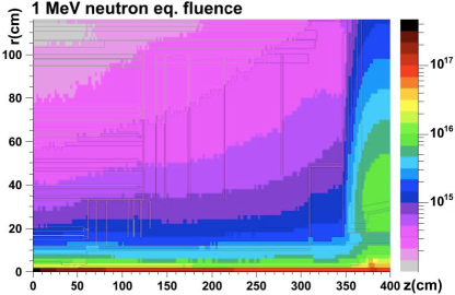
The ATLAS pixel detector is composed of 250 m thick n-in-n DOFZ-Si pixel sensors with cell sizes of m2, readout by the DC-coupled (bump-bonded) FEI3 chips [4]. It has been designed to withstand a fluence of , which will be exceeded in the inner layer before the end of phase I. For this reason, a fourth pixel layer (IBL [5]) at cm will be inserted during the 2013-2014 shutdown and is designed to withstand a total fluence of ( including safety factors). The whole pixel detector will be replaced before the start of phase II, in order to cope with the increased occupancy (between 100 and 200 pile-up collisions, an order of magnitude higher than at the nominal LHC luminosity) and radiation damage, with the innermost layer being exposed to a total fluence of (Fig. 1).
2 The ATLAS Upgrade PPS Collaboration
The LHC upgrade poses several challenges to the ATLAS pixel detector:
-
•
radiation damage: the much higher fluences imply increased leakage currents, a higher bias voltage needed to (at least partially) deplete the devices, and larger charge trapping (lower charge collection efficiency). S/N will decrease.
-
•
data rate: the higher interaction rate requires smaller pixels to keep occupancy under control. Pixels of size m2 are being produced for the IBL, even smaller pitches may be used for the inner layers for the phase II upgrade. For the same reason, the replacement of the innermost short strip layer(s) by pixel layer(s) might be desirable, however, a significant cost reduction of pixel sensors is necessary to compete with strip sensor costs.
-
•
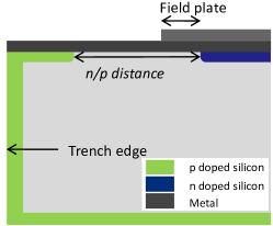
tight geometrical constraints: with the addition of a fourth pixel layer closer to the beampipe, the limited space between the first layers will not allow the ”shingling” of the detector modules along the beam direction. In addition, flat staves ease cooling and production. To minimize the geometric efficiency losses the edges of the modules have to be active or at least slimmer (m) than the current ones. The inactive edge of the present modules is 1.1 mm, hosting 16 guard rings (total width m) to manage the potential drop between the cutting edge of the sample and the pixel electrodes, and an additional safety margin of 500 m to insulate the guard ring area from damages of the lateral surface due to the dicing.
To investigate the suitability of pixel sensors using the proven planar technology, already exploited successfully in ATLAS and other high-energy-physics (HEP) experiments at colliders, for the upgraded tracker, the ATLAS Planar Pixel Sensor R&D Project was established [6]. It is formed by more than 80 scientists from 17 European, US and Japanese institutes. Main areas of research are the performance of planar pixel sensors at phase I and II fluences, the exploration of possibilities for cost reduction to enable the instrumentation of large areas, the achievement of slim or active edges to provide low geometric inefficiencies without the need for shingling of modules and the investigation of the operation of highly irradiated sensors at low thresholds to increase the efficiency. Several test prototypes have been produced at various foundries (CiS, Micron, Hamamatsu, MPI-HLL) in collaboration with RD50 [7] and characterized by probe station (IV/CV curves), with radioactive sources, and in testbeams with pions at CERN and electrons at DESY (hit efficiency, charge collection), before and after irradiations. Both neutron irradiation (with the Triga reactor in Ljubljana) and proton irradiation (using a 23 MeV/c beam in Karlsruhe and the 24 GeV/c beam of the CERN PS) have been performed. The optimization of some of the sensor parameters, for instance the geometrical guard ring (GR) configuration (number of GRs, widths, distances), has been supported by the use of TCAD electrical simulation tools [8, 9]. In the following sections we summarize the most recent results of these ongoing R&D studies.
3 Radiation hardness of -type and -type pixel sensors
Only electron-collecting sensors designs (n-in-p and n-in-n) have been considered in the PPS R&D, for two radiation damage related reasons: the hole trapping time is unacceptably short at large fluences, and p-in-n (after type inversion) and p-in-p sensors cannot be operated efficiently at partial depletion because of the undepleted volume near the electrodes.
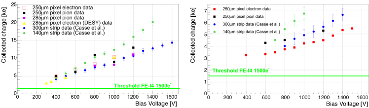
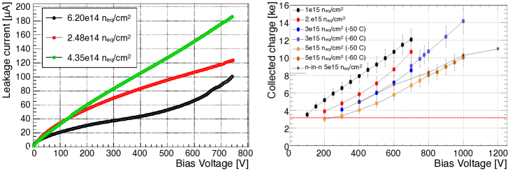
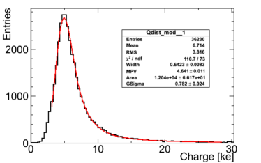
The radiation hardness of n-in-n prototypes has been tested after neutron irradiations up to fluences of n. Operating temperatures of C have been chosen to reduce the leakage current and therefore shot noise. Testbeam data on devices connected to readout chips tuned for thresholds of 1500 e show that about half (10 ke) of the charge deposited by a MIP in 250 m of Si can be collected with a bias voltage of 1 kV, which is the maximum allowed for the IBL at the end of the LHC phase I, after n (Fig. 2, left). This translates into a signal-over-treshold ratio and a signal-to-noise ratio . Similar studies show that some charge (around 5.5 ke) can be collected even at n by increasing the bias voltage to 1.5 kV (Fig. 2, right).
Preliminary measurements of the hit efficiency in 250 m thick, n-in-n irradiated sensors performed in the June 2011 testbeam at the CERN SPS [11] (Fig. 3) show that already at an efficiency greater than 97% can be achieved after neutron irradiation to n.
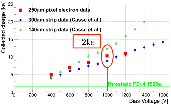
In recent years the interest for p-bulk devices as possible sensors for HEP experiments has rapidly increased as high-resistivity p-type wafers have become available and since they do not undergo type inversion after heavy irradiation. Moreover, since guard rings are located on the same side as the pixel electrodes, the layout of these sensors requires a single sided production process with less steps than for n-in-n sensors, and possible cost reduction. A potential issue is that since the GRs are on the same side as the pixels, which are connected to the front end electronic chip which is at ground, the full bias voltage is right at the edge of the sensor and only a few m away from the chip. The high bias voltages needed to deplete the sensors may thus generate sparks that would destroy the chip. With an additional passivation layer ( 3 m) of a highly insulating material like benzocyclobutene or parylene on top of the sensors this effect has not been observed for bias voltages up to 1 kV. Recently 285 m thick n-in-p sensors were produced at CiS and bump-bonded to FEI3 chips at IZM-Berlin. Prior to irradiation they exhibited breakdown voltage much higher than the full depletion voltage (60 V), leakage currents around 500 nA/cm2 (unaffected by bump-bonding), narrow threshold tuning with a mean of 3200 e and dispersion 22 e and 100% charge collection efficiency at full depletion. S/N ( 19) and hit efficiency (¿99%, measured in testbeams) were similar to that of n-in-n pixels (and of n-in-p sensors produced by HPK and Micron). These devices have been subsequently tested after irradiation with either protons or neutrons. After a fluence of about n, the breakdown voltage is greater than 750 V and the leakage current lower than 200 A at C (Fig. 4, left). A significant fraction (¿30%) of the charge generated by a MIP is collected at a high bias voltage (¿600 V) and yields a detectable signal above threshold (Fig. 4, right). The charge collection efficiency is similar to that of n-in-n devices exposed to similar hadron fluences.
4 Sensor thinning
Recent strip-sensor data show that thinner sensors yield more charge than thicker ones after fluences of n for bias voltages of 1 kV or higher, because of the higher electric field and possibly also due to charge multiplication inside the bulk [10]. Thinner sensors for HEP experiments have the additional advantage of the lower material budget, which improves momentum resolution and reduces energy loss in front of downstream detectors. Recently CiS has started to produce for the PPS R&D n-in-n sensors with thicknesses between 150 and 250 m, in steps of 25 m. Part of the 250 m sensors have been delivered, with good wafer yield (90%) and sensor-on-wafer yield close to 100%. At V kV they collect more charge than 300 m thick strips (Fig. 5). Similar studies will be performed on the thinner sensors as soon as they become available. Also n-in-p sensors with thicknesses of 150 and 200 microns are being produced by the same vendor and will be tested in the near future.
5 Reducing the inactive area with slim-edge or active-edge devices
To avoid that the depletion region spreading from the active area reaches the damaged lateral surface, an undepleted region is usually present at the sensor’s edge. This inactive area reduces charge collection near the edge. To increase the active area we are exploring two techniques.
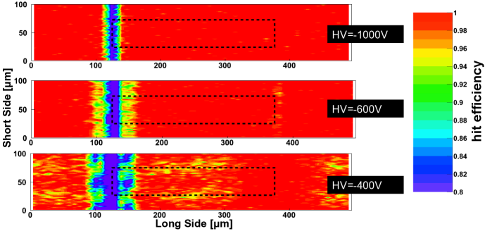
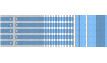
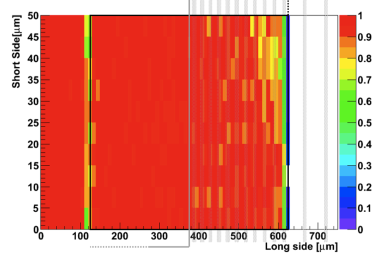
Edges can be made ”slim” by reducing both the width of the guard ring area, optimizing the number and spacing of the GRs, and the safety margin, exploiting dicing techniques that create less surface damage. Based on simulations and on several dicing trials showing a good yield, a reduced number of 13 guard rings with a safety margin of 100 m was proposed for the IBL sensors. A further gain for n-in-n pixels can be obtained by extending the pixel implants, which are located on the side opposite to the GRs, to partially overlap the guard rings (Fig. 6, left). In the overlap region the bulk is (at least partially) depleted and sufficient charge is collected, with a reduction of the inactive area to less than 1.5%. This has been investigated with n-in-n slim-edge sensors in a recent testbeam at CERN. Preliminary results show a high efficiency (close to 100%) up to about 250 m from the cutline for non-irradiated devices as well as for devices irradiated with neutrons up to n and biased at 1 kV (Fig. 6, right) [12]. Given the good performance and yields achieved, the slim-edge design has been chosen as the IBL candidate technology for the planar pixels and is currently being produced.
A second technique for the reduction of the inactive area is the active-edge concept. Within the PPS R&D two technologies are being investigated. The former, proposed in [13] and available at several foundries collaborating with the PPS group (CNM, FBK, VTT), uses Deep Reactive Ion Etching (DRIE) to obtain deep trenches around the detectors, thus eliminating the need of the cutting procedure. These trenches are heavily doped so as to behave like ohmic contacts (Fig. 7, left). The fabrication process requires a support wafer and presents technological challenges in the excavation of deep (200-230 m) trenches with aspect-ratio around 1:20 and in filling the trenches with polysilicon with good planar surface, as needed for proper deposition of the photoresist for the later production stages. Preliminary measurements on test diodes produced at FBK with this technique show reasonably low leakage currents and breakdown voltages higher than the full depletion value. [14]. A production of planar pixel sensors with this technique is currently being planned. The second edgeless technology is based on laser scribing and cleaving, which result in significantly less surface damage [15] thus eliminating the need for a safety margin, and on passivation of the lateral surface with either silicon oxide or nitride (for n-type bulk sensors) or atomic layer deposition (ALD) of aluminum oxide (for p-type bulk). This creates an interface charge (positive for silicon oxide and negative for aluminum oxide) on the lateral surface that is able, if its density is sufficiently high (around cm-2), to guarantee that the potential drop at the edge is negligible even without guard rings. Using the U.S. Naval Research Laboratory facilities for laser scribing and ALD, diodes without guard rings and a distance of only 14 m between the active area and the cutting edge were produced (Fig. 7, right). These diodes show no evidence of breakdown up to 1 kV and a charge collection efficiency close to 100% even near the edge. In the future several tests are planned, in particular to assess the radiation hardness of these technologies.

6 Other activities
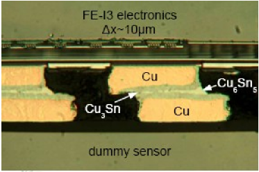
The phase II ATLAS Inner Detector may exploit an additional pixel layer at larger radius in order to improve tracking performances; some of the strip layers may also be replaced by pixels to reduce the occupancy. The planar technology could be exploited since the expected fluences at those radii will not exceed a few 1015 neq/cm2. Because the instrumented area will be much larger than in the current pixel detector, cost efficiency becomes a major concern. On the sensor side, possible cost-saving measures include using 6” instead of 4” wafers and n-in-p instead of n-in-n sensors. However, most of the cost of the ATLAS pixel detector was due to the bump bonding of the front-end electronic chips to the sensors. For this reason, an alternative technique based on Solid-Liquid InterDiffusion (SLID [16]) has started to being investigated recently, in collaboration with Fraunhofer Institute (IZM Munich). A (pixelated) thin (5 m) layer of copper (Cu) is deposited through mask electroplating on both the sensors and the chip. In addition, a 3 m layer of tin (Sn) is overlaid on top of the Cu on the sensor. The sensors and the chip surfaces are brought into contact in a controlled environment where a temperature around 300 C and a pressure around 5 bar is reached. At such temperatures the tin melts and an eutectic alloy (CuxSny) contact is formed. The alloy has a melting temperature greater than 600 C and therefore does not liquify during the process. This technique should be cheaper than standard bump-bonding as it requires less processing steps. It should also be exploitable with small pitches and stacking. First results with thin (75 m) n-in-p pixels connected to FEI3 chips showed promising results, with threshold dispersion, noise and charge collection efficiency comparable to those of bump-bonded sensors. Sporadic problems with chip misalignment and a few disconnected channels are under investigation.
7 Conclusion
Extensive R&D by the PPS group has demonstrated that the proven planar technology of the ATLAS pixel detector is well suited even at the fluence ( neq/cm2) predicted for the innermost layer in the phase I upgrade. The planar pixel sensors have been shown to operate and collect some charge even at phase II fluences ( neq/cm2). Encouraging results have been obtained also in terms of reduction of costs and of the inactive regions at the edge. Further activities are planned in the future in order to evaluate the performances of thinner detectors and to establish the radiation hardness up to neq/cm2 of the various technologies under consideration.
References
- [1] ATLAS Collaboration, The ATLAS Experiment at the CERN Large Hadron Collider, JINST 3 (2008) S08003.
- [2] ATLAS Pixel Collaboration, ATLAS pixel detector electronics and sensors, JINST 3 (2008) P07007.
- [3] F. Gianotti et al., Physics potential and experimental challenges of the LHC luminosity upgrade, Eur. Phys. J. C 39 (2005) 293.
- [4] I. Peric et al., The FEI3 readout chip for the ATLAS pixel detector, Nucl. Instrum. Meth. A 565 (2006) 178.
- [5] ATLAS Collaboration, ATLAS Insertable B-Layer Technical Design Report, CERN-LHCC-2010-013, ATLAS-TDR-019 (2010).
- [6] ATLAS Upgrade PPS Collaboration, R&D on planar pixel sensor technology for the ATLAS Inner Detector upgrade (PPS proposal), CERN. https://edms.cern.ch/document/966140.
- [7] RD50 Collaboration, http://rd50.web.cern.ch/rd50/
- [8] Silvaco International Inc., 4701 Patrick Henry drive, Bldg. 1, Santa Clara, CA 95054. www.silvaco.com
- [9] G. Calderini et al., Simulations of planar pixel sensors for the ATLAS high luminosity upgrade, Nucl. Instrum. Meth. A 636 (2011) S37.
- [10] G. Casse, Charge multiplication in highly irradiated planar silicon sensors, PoS VERTEX2010 (2010) 020.
- [11] ATLAS IBL Collaboration, Test beam characterization of pixel sensors for the ATLAS Insertable B Layer Upgrade, article in preparation.
- [12] S. Altenheiner et al., Planar slim edge ATLAS pixel sensors for the IBL and high-lumi-LHC upgrades (proceedings of the PSD9 conference), submitted to JINST.
- [13] C. J. Kenney et al., Results From 3-D Silicon Sensors With Wall Electrodes: Near-Cell-Edge Sensitivity Measurements as a Preview of Active-Edge Sensors, IEEE Trans. Nucl. Sci. NS-48 (6) (2001), 2405.
- [14] M. Povoli et al., Development of planar detectors with active edge, Nucl. Instrum. Meth. A, article in press. http://dx.doi.org/10.1016/j.nima.2011.04.050
- [15] Z. Li et al., Electrical and Transient Current Characterization of Edgeless Si Detectors Diced With Different Methods, IEEE Trans. Nucl. Sci. NS-49 (3) (2002), 1040.
- [16] A. Klumpp et al., Vertical System Integration by Using Inter-Chip Vias and Solid-Liquid Interdiffusion Bonding, Jpn. J. Appl. Phys. 43 (2004) L829.