Disorder induced metallicity in amorphous graphene
Abstract
We predict a transition to metallicity when a sufficient amount of disorder is induced in graphene. Calculations were performed by means of a first principles stochastic quench method. The resulting amorphous graphene can be seen as nanopatches of graphene that are connected by a network of disordered small and large carbon rings. The buckling is minimal and we believe that it is a result of averaging of counteracting random in-plane stress forces. The linear response conductance is obtained by a model theory as function of lattice distortions. Such metallic behaviour is a much desired property for functionalisation of graphene to realize a transparent conductor, e.g. suitable for touch-screen devices.
pacs:
laterSince the discovery of graphene, and all its unique physical properties first ; r1 ; r2 ; r3 ; r4 , attention is now turned to functionalization of this material to suit specific applications. One example is the suggestion of graphane, where H atoms are adsorbed on graphene. Graphane, which is an insulator, was predicted from first principles theory graphane1 , and was subsequently realized experimentally elias . Further theoretical works graphane2 ; graphane3 addressed e.g. the value of the band gap, which was found to be of order 5.7 eV. In a similar fashion, fluorine can also be found to adsorb, and in theoretical works a band gap of 7.4 eV is found graphxene1 ; belgian , which is larger than the measured value of 3.4 eV graphxene2 . The reason that a large band gap opens up when hydrogen or fluorine is adsorbed on graphene is that sp2 bonded C atoms become sp3 bonded. Hence it seems possible to decrease the conductivity by chemical functionalization, and turn the semi-metallic graphene to a semi-conductor or even an insulator. Smaller values of the gap can be reached by a functionalization by organic molecules BK2010 .
The ways to increase the conductivity by chemical means has also been discussed, although here significantly less success can be identified. Adsorption by single impurities wehling have been explored, as well as the replacement of C atoms for B or N atoms biplab , or even the creation of structural defects in the C matrix victoria ; jafri ; karel . The electronic structure of non-crystalline graphene, e.g. around grain boundaries have also been under consideration, both from tight-binding analysis malola and within the framework of first principles theory louie in combination with calculations of transport properties. In the works mentioned above, the conducting properties are still those of a doped semiconductor, with relatively few charge carriers. A fully metallic behavior was however suggested in an amorphous structure of graphene kapko , where Stone-Wales defects were introduced into graphene and geometry optimization was done according to a Keating-like potential. After geometry optimization, the electronic structure was calculated from a tight-binding Hamiltonian, and a non-zero value of the density of states (DOS) at the Fermi level (EF) was obtained, suggesting that metallic conductivity is possible. The possibility of a transparent, mono-atomic thin material, has a great potential in applications involving touch screens and electronics ITO . Very recently, the two-dimensional amorphous carbon has been derived experimentally by electron beam irradiation Kotakoski et al. (2011). In this paper we study its electronic structure with a first-principles based approach, which accurately described both the chemical bonding and structural properties, as well as the electron energy spectrum.
The amorphous graphene structures were obtained by means of a stochastic quenching method Holmström et al. (2009, 2010). The method is well adapted to describe amorphous structures that have been obtained by ultra-fast cooling, such as e.g. sputtered amorphous films where the structure has been realized directly from the gas phase Århammar et al. (2011). It can also be used to describe the most typical amorphous structures of a material in order to find reliable parameters for a Hamiltonian description of the liquid state Bock et al. (2010). Normally, this technique is used for calculations of amorphous structures in bulk where the atoms are first placed randomly in the calculation cell and then the positions are relaxed by means of a conjugate gradient method until the force on every atom is zero. In the present case we confined the atoms to the plane in order to find a reliable description of the two-dimensional amorphous structure. First, 200 atoms were placed at random positions in the plane with an average density equal to that of graphene. We then relaxed the positions of all atoms, while enforcing that all atoms should stay in-plane. Then the area of the plane was relaxed until the pressure upon the cell was zero. At this point we obtained the structure called ”basic planar”. The area relaxation resulted in new forces on the atoms so we had to repeat the position and area relaxations until both the pressure and forces were minimized. At this point we obtained the structure called ”final planar”. The relaxation of positions was then allowed to take place in 3 dimensions and the process of area and position relaxation cycling was repeated until the in-plane stress and all forces on the atoms were minimized again. At this point we obtained the structure called ”buckled”.
The first principles, self-consistent electronic structure calculations were performed by means of density functional theory Kohn and Sham (1965) using the projected augmented wave method Blöchl (1994) as implemented in the Vienna ab initio simulation package (VASP) code Kresse and Furthmüller (1996). The geometry optimizations have been performed without any symmetry constraint and using the conjugated gradient algorithm. A plane wave energy cutoff of 300 eV was used for the structural relaxations whereas 500 eV was used for the DOS and total energy calculations. The Perdew-Wang Perdew and Wang (1992) parametrization of the generalized gradient approximation of the exchange-correlation interaction was used. For sampling the irreducible Brillouin zone the point was used for the relaxations whereas a 5x5x1 mesh of 13 k-points was used for the DOS and total energy calculations. The amount of vacuum in the supercell was chosen to avoid artificial surface-surface interactions (24 Å). In all relaxations, convergence was achieved when the force on each ion was less than 10-2 eV/Å.
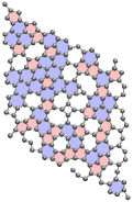
The basic planar configuration that was obtained after the first position-area relaxation cycle is shown in Figure 1(a). We can see that this structure consists of 23 hexagonal and 56 pentagonal, some tetragonal and triangular rings. There are also some areas with larger rings of up to 8 atoms. This structure is still very compressed since the area is still close to that of graphene. We can see that a large number of carbon atoms are both 4 and 5-fold coordinated, which indicates a frustrated state of high energy. The total energy per atom of this structure is 1.50 eV larger than the graphene reference. Further iterations of positions and area relaxations resulted in the final planar structure shown in Figure 1(b). The number of hexagonal rings has now increased to 38 and the number of pentagonal rings decreased to 25. Several larger rings have appeared with up to 9 atoms. All carbon atoms are now 3-fold coordinated and hence sp2 bonded, except in 2 cases where the coordination is 2-fold with a 180∘ bond angle and hence the bonding is sp. There is also one atom in the lower edge of the figure that is bonded to only one other atom. The total energy per atom of this structure is now 0.50 eV larger than the graphene reference.
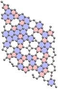
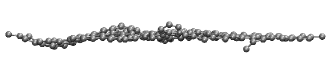
The position and area relaxation of the final planar structure was taken further by letting the atoms relax also in the direction normal to the plane. The resulting buckled structure is shown in Figure 1(c) and a side view can be seen in Figure 1(d). From the side view we can see that the plane has evolved into a weakly oscillating shape. In this structure the number of pentagonal and hexagonal rings has not changed compared to the final planar structure. The atom with only one bond is also present in this structure and it can be seen in Figure 1(d) where it protrudes out below the surface. The total energy of the buckled system was 0.43 eV larger per atom than the total energy of the graphene reference. This structure must be considered as an archetype structure amonst many possible realizations of amorphous graphene. There may even exist lower energy amorphous states than the one we have found here. The amorphous state that we have found is surprisingly flat and contains both squares and triangles. We speculate that the flatness is due to an averaging of defect-induced buckling forces. Square geometries have recently been observed in defect rich graphene that was created by electron irradiation Kotakoski et al. (2011).

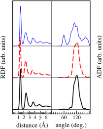
The radial and angle distribution functions are shown in Figure 2(a). We can see that the first peak in all radial distribution functions is located at 1.4 Å. However, the radial distribution function of the basic planar structure has somewhat broader peaks than the other structures. The angle distribution functions show a much larger difference. Here the basic planar structure shows three pronounced peaks around 60, 110, and 160 degrees whereas the final planar and buckled structures show one pronounced peak around 120 degrees and only small quantities of 60 and 90 degree angles.
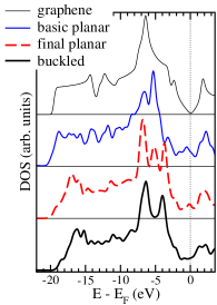
The total DOS for graphene and the three amorphous geometries are shown in Figure 2(b). We can see that the basic planar structure has somewhat broader bands but the widths of the final planar and buckled structure are somewhat narrower than graphene. The largest difference is however around the Fermi level where the amorphous structures have high enough density of states to be clearly metallic.
The realization of a metallic DOS for a monolayer-thick graphene material is a significant result, and the transport properties of this system requires further analysis. We do this by a model theory, as described below. We consider the case of an imperfect 2D carbon lattice where all C atoms are interconnected to three other C atoms and consider it to be bipartite. In the spirit of a nearest neighbor model, we have as a Hamiltonian of the system jafri
| (1) |
where , operators and annihilate electrons in sublattices A and B, respectively. At each site , we express the spatial vectors to the neighboring sites , can be expressed in terms of and additional piece , i.e. . Assuming that the random vector connecting sites and are independent of the specific location in the lattice, we can simplify the random vector to depend only on . This allows the calculation , so that we can define . The Hamiltonian is thereby reduced to
| (2) |
Next, we assume that the random vector , , is normal distributed with mean and variance . Also, by assuming that the random variables and are independent, we can replace the exponential by . As mean values of the random vectors, we take a set of basic lattice vectors for graphene, e.g. , , and , and we assume that . For structures with only small variations from the perfect graphene lattice, we can expand around the points , around which the dispersion relation for graphene is linear, i.e. , where and . Expanding the potential around , retaining contributions of quadratic order in at most, we obtain
| (3) |
where we have introduced and , whereas . The scattering potential converges to the usual graphene potential as the variance , as required. The above expression for the scattering potential holds for small distortions from the ideal graphene lattice. Quantitatively we require that , where is a high energy cut-off, giving .
Numerically, we find that the dispersion given in Eq. (3) is applicable for lattice distortions up to about , see Fig. 3 (a), where we plot the computed bands when applying the stochastic arguments to the model given in Eq. (2). Around , the dispersion is basically linear for rather large lattice distortions, and the DOS resulting from the band structure, Fig. 3 (b), shows the typical linear characteristics around the Fermi level () for small lattice distortions (). Here, the DOS () is calculated in terms of the Green function is defined in terms of the eigenbasis given by the Hamiltonian in Eq. (2).
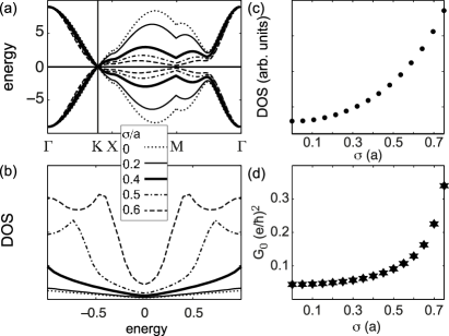
In Fig. 3 (c), we plot the DOS resulting from the approximate dispersion in Eq. (3), showing a monotonic increase with the lattice distortion, as expected.
For further investigations of the potential metallicity of the amporphous graphene, we also calculate the linear response conductance, , using the Kubo formalism. For an electric field applied in the -direction, we use
| (4) |
where , and . Neglecting vertex corrections, we calculate the d.c. conductance at zero temperature according to
| (5) |
We obtain a monotonically increasing conductance as the distortion of the lattice increases, see Fig. 3 (d), which supports the conclusion that our two-dimensional amorphous carbon lattice is metallic. The same conclusion is drawn from the approximate model based on the dispersion relation in Eq. (3).
In summary, we have performed first principles theory as well as considered a model Hamiltonian, to demonstrate that graphene can become metallic, once a significant disorder is introduced in the material. In the present work, this has been achieved by a realistic amorphization in 3 dimensions, using the stochastic quenching method. Our results show a transition from the complex electronic structure associated with perfectly crystalline graphene to a regular conducting behavior. This transition occurs rather drastically as a function of the amount of disorder in the materials. Experimentally, disorder and non-crystallinity is commonly obtained by ion-irradiation of a crystalline material, or by rapid thin-film growth, and it is likely that this is an experimental way forward also in this case. The energy associated with some of the amorphous structures considered here is only 0.43 eV/atom higher than that of crystalline graphene.
If realized experimentally, a much desired metallic and transparent thin film has been found, with the possibility to have impact in applications, e.g. in touch screens. Given that other allotropes of C can become superconducting, at least when doped, this may also be explored for amorphous graphene.
Calculations were performed on Ainil, the supercomputer at the physics institute at UACH funded by Chilean FONDECYT projects 1110602 and 11080259. Financial support by the EU-India FP-7 collaboration under MONAMI is acknowledged, as well as the Swedish Research Council (VR), the foundation for strategic research (SSF), the European Research Council (ERC), the KAW foundation and the Swedish National Infrastructure for Computing (SNIC). JF thanks Allan Gut for fruitful discussions.
References
- (1)
- (2) K. S. Novoselov et al, Science 306, 666 (2004).
- (3) A. K. Geim and K. S. Novoselov, Nature Mater. 6, 183 (2007).
- (4) M. I. Katsnelson, Mater. Today 10, 20 (2007).
- (5) A. H. Castro Neto, F. Guinea, N. M. R. Peres, K. S. Novoselov, and A. K. Geim, Rev. Mod. Phys. 81, 109 (2009).
- (6) M. A. H. Vozmediano, M. I. Katsnelson, and F. Guinea, Phys. Rep. 496, 109 (2010).
- (7) J. O. Sofo, A. S. Chaudhari, and G. D. Barber, Phys. Rev. B 75, 153401 (2007).
- (8) D. C. Elias et al. Science 323, 610 (2009).
- (9) D. W. Boukhvalov, M. I. Katsnelson, and A. I. Lichtenstein, Phys. Rev. B 77, 035427 (2008).
- (10) S. Lebègue, M. Klintenberg, O. Eriksson, M. I. Katsnelson, Phys. Rev. B 79, 245117 (2009).
- (11) M. Klintenberg, S. Lebègue, M. I. Katsnelson, and O. Eriksson, Phys. Rev. B 81, 85433 (2010).
- (12) O. Leenaerts, H. Peelaers, A. D. Herna’ndez-Nieves, B. Partoens, and F. M. Peeters, Phys. Rev. B 82, 195436 (2010).
- (13) R. R. Nair et al, Small 6, 2877 (2010).
- (14) D. W. Boukhvalov and M. I. Katsnelson, J. Phys. D 43, 175302 (2010).
- (15) T. O. Wehling, M. I. Katsnelson, and A. I. Lichtenstein, Chem. Phys. Lett. 476, 125 (2009); T. O. Wehling, M. I. Katsnelson, and A. I. Lichtenstein, Phys. Rev. B 80, 085428 (2009); T. O. Wehling, S. Yuan, A. I. Lichtenstein, A. K. Geim, and M. I. Katsnelson, Phys. Rev. Lett. 105, 056802 (2010).
- (16) B. Sanyal, O. Eriksson, U. Jansson, and H. Grennberg, Phys. Rev. B 79 113409 (2009).
- (17) V. A. Coleman, R. Knut, O. Karis, H. Grennberg, U.Jansson, R. Quinlan and B. C. Holloway, B. Sanyal, and O. Eriksson, J. Phys. D: Appl. Phys. 41 (2008) 062001.
- (18) S. H. M. Jafri et al, J. Phys. D: Appl. Phys. 43, 045404 (2010).
- (19) K. Carva, B. Sanyal, J. Fransson, and O. Eriksson, Phys. Rev. B 81, 245405 (2010).
- (20) S. Malola, H. Häkkinen, and P. Koskinen, Phys. Rev. B 81, 165447 (2010).
- (21) O. V. Yazyev and S. Louie, Nature Materials 9, 806 (2010).
- (22) V. Kapko, V. A. Drabold, and M. F. Thorpe, Physica Status Solidi 247, 1197 (2010).
- (23) David S. Ginley in ”Handbook of Transparent Conductors” Springer (New York, Heidelberg).
- Kotakoski et al. (2011) J. Kotakoski, A. V. Krasheninnikov, U. Kaiser, and J. C. Meyer, Phys. Rev. Lett. 106, 105505 (2011).
- Holmström et al. (2009) E. Holmström, N. Bock, T. B. Peery, R. Lizárraga, G. De Lorenzi-Venneri, E. D. Chisolm, and D. C. Wallace, Phys. Rev. E 80, 051111 (2009).
- Holmström et al. (2010) E. Holmström, N. Bock, T. Peery, E. Chisolm, R. Lizárraga, G. De Lorenzi-Venneri, and D. Wallace, Phys. Rev. B 82, 024203 (2010).
- Århammar et al. (2011) C. Århammar, A. Pietzsch, N. Bock, E. Holmström, C. M. Araujo, J. Grasjo, S. Zhao, S. Green, T. Peery, F. Hennies, et al., Proceedings of the National Academy of Sciences 108, 6355-6360 (2011).
- Bock et al. (2010) N. Bock, E. Holmström, T. B. Peery, R. Lizárraga, E. D. Chisolm, G. De Lorenzi-Venneri, and D. C. Wallace, Phys. Rev. B 82, 144101 (2010).
- Kohn and Sham (1965) W. Kohn and L. Sham, Phys. Rev. 140, A1133 (1965).
- Blöchl (1994) P. E. Blöchl, Phys. Rev. B 50, 17953 (1994).
- Kresse and Furthmüller (1996) G. Kresse and J. Furthmüller, Phys. Rev. B 54, 11169 (1996).
- Perdew and Wang (1992) J. P. Perdew and Y. Wang, Phys. Rev. B 45, 13244 (1992).