Robust zero-averaged wave-number gap inside gapped graphene superlattices
Abstract
In this paper, the electronic band structures and its transport properties in the gapped graphene superlattices, with one-dimensional (1D) periodic potentials of square barriers, are systematically investigated. It is found that a zero averaged wave-number (zero- ) gap is formed inside the gapped graphene-based superlattices, and the condition for obtaining such a zero- gap is analytically presented. The properties of this zero- gap including its transmission, conductance and Fano factor are studied in detail. Finally it is revealed that the properties of the electronic transmission, conductance and Fano factor near the zero- gap are very insensitive to the structural disorder for the finite graphene-based periodic-barrier systems.
pacs:
73.61.Wp, 73.20.At, 73.21.-bI Introduction
Graphene, a single layer of carbon atoms densely packed in a honeycomb lattice, has attracted a lot of research interest due to its remarkable electronic properties and its potential applications Novoselov2004 ; Zhang2005 ; Novoselov2005a ; Berger2006 ; Katsnelson2006 ; reviews . Inside the pristine graphene, the low-energy charge carriers can be formally described by a massless Dirac equation, and near Dirac point one has discovered many intriguing properties, such as the unusual energy dispersion, the chiral behavior Katsnelson2006 ; Katsnelson2006b , ballistic charge transport Miao2007 ; Du2008 , Klein tunneling Cheianov2006 , and unusual quantum Hall effect Novoselov2005a ; Purewal2006 ; Neto2006 , bipolar supercurrent Heersche2007 , frequency-dependent conductivity Kuzmenko2008 , gate-tunable optical transitions Wang2008 , and so on.
However, for applications of graphene to nanoelectronics, it is crucial to generate a band gap in Dirac spectrum in order to control the electronic conductivity, such as a channel material for field-effect transistor. For realizing this purpose, several approaches are studied both theoretically and experimentally. One of them is using the quantum confinement effect in graphene nanoribbons Son2006a ; Son2006b ; Han2007 and graphene quantum dots Trauzettel2007 . It has been shown that the size of the gap increases as the nanoribbon width decreases and it also strongly depends on the detailed structure of the ribbon edges. An alternative method is spin-orbit coupling, which also leads to generate a small gap due to both intrinsic spin-orbit interaction or the Rashba interaction Kane2005 ; Min2006 ; Yao2007 . Another approach is substrated-induced band gaps for graphene supported on boron nitride Giovannetti2007 or SiC Zhou2007 ; Kim2008 by making the two carbon sublattices (A and B sublattices) inequivalent; and with this approach, a gap of 260meV is experimentally demonstrated Zhou2007 . Therefore the quasiparticles in the graphene grown on a SiC or boron nitride substrate behave differently from those in the graphene grown on SiO2. The effect of sublattice symmetry breaking on the induced gap is also systematically investigated Qaiumzadeh2009 . There are also theoretical works to engineer the tunable bandgap by periodic modulations of the graphene lattice via the hydrogenation of graphene Duplock2004 , and a recent experiment demonstrates that patterned hydrogen adsorption on graphene induces a bandgap of at least 450meV around the Fermi level Balog2010 .
Since superlattices are very successful in controlling the electronic structures of many conventional semiconducting materials (e.g. see Ref. Tsu2005 ), the devices of graphene-based superlattices has attracted much attention. It can be the periodic potential structures generated by different methods, such as electrostatic potentials Bai2007 ; Park2008b ; Barbier2008 ; Park2008a ; Barbier2009 ; Tiwari2009 and magnetic barriers RamezaniMasir2008 . In gapless graphene-based superlattices, researchers have found that a one-dimensional (1D) periodic-potential superlattice possesses some distinct electronic properties, such as the strong anisotropy for the low-energy charge carriers’ group velocities Park2008b , the formation of the extra Dirac points and new zero energy states Brey2009 ; Park2008a , and the unusual properties of Landau levels and the quantum Hall effect for these extra Dirac fermions Park2009 . From the previous studies Barbier2008 ; Barbier2010 ; LGWang2010 ; Arovas2010 ; Ho2009 , one has known that for the gapless graphene superlattices there is no gap opening at the normal incidence due to the Klein tunneling. Most recently, the new electronic properties in gapped graphene-based devices are discovered since the Klein tunneling is suppressed due to the presence of a gap Gomes2008 ; Soodchomshom2009 ; Jiang2010 ; Esmailpour2010 ; Guinea2010 .
All the above investigations stimulate us to study how the electronic properties and bandgap structures of the grapped graphene superlattices are affected due to a gap opening at the Dirac point, and what properties are derived for the gapped graphene superlattices that are different from the gapless graphene superlattices. In our previous work LGWang2010 , we have found that a new Dirac point is formed at the energy which corresponds to the zero averaged wave-number inside the gapless graphene-based superlattices. In this paper, we will continue to investigate the electronic band structures and their transport properties for the gapped graphene superlattices with 1D periodic potentials of square barriers. We find that a zero averaged wave-number (zero-) gap is formed inside the gapped graphene-based superlattices, which is very similar to the zero-averaged refractive-index gap in 1D photonic crystals consisted of left-handed and right-handed materials Li2003 . The properties of this zero- gap are detailed studied, and the related electronic transmission, conductance and Fano factor near the zero- gap in the finite graphene superlattices are further illustrated.
The outline of this paper is the following. In Sec. II, we introduce a transfer matrix method to calculate the reflection and transmission for the gapped graphene superlattices. In Sec. III, we first discuss the electronic band structures for the infinite gapped graphene-based periodic-barrier superlattices, and then we investigate the changes of the transmission, conductance and Fano factor for the finite superlattices and the effects of the structural disorders on the electronic properties are also discussed in detail. Finally, in Sec. IV, we summarize our results.
II Transfer Matrix method for the gapped mono-layer graphene superlattices
We consider a mono-layer graphene with a peculiar gap due to the sublattice symmetry breaking or the intrinsic spin-orbit interaction. In this situation, the Hamiltonian of an electron in the presence of the electrostatic potential , which only depends on the coordinate , is given by Esmailpour2010 ; Qaiumzadeh2009b
| (1) |
where is the momentum operator with two components, , and and are Pauli matrices, is a unit matrix, and m/s is the Fermi velocity. Here is the energy gap due to the sublattice symmetry breaking Zhou2007 , or is the energy gap due to the intrinsic spin-orbit interaction Kane2005 . From the experimental data, we know that the maximum energy gap could be 260meV due to the sublattice symmetry breaking Zhou2007 .
The above Hamiltonian acts on the state of a two-component pseudo-spinor, where and are the smooth enveloping functions for two triangular sublattices in the mono-layer graphene, and the symbol ”” denotes the transpose operator. In the direction, because of the translation invariance, the wave functions can be factorized by Therefore, from Eq. (1), we obtain
| (2) | |||||
| (3) |
where are the transit (or coupled) parameters from () to (), is the incident electron energy, and corresponds to the incident electronic wavenumber. When , the above two equations reduce to the cases in Refs. Barbier2010 ; LGWang2010 ; Arovas2010 .
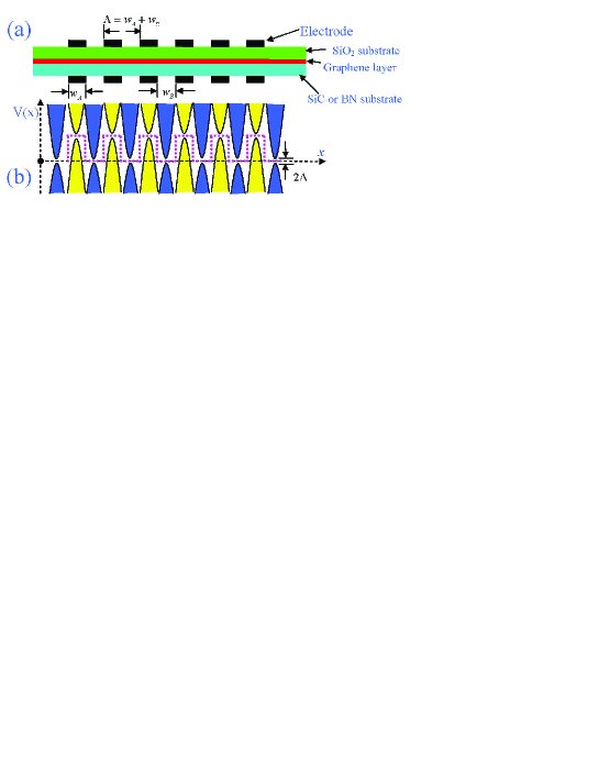
For the gapped graphene superlattices, we assume that the potential is comprised of periodic potentials of square barriers as shown in Fig. 1. Inside the th barrier, is a constant, therefore, from Eqs. (2) and (3), we have
| (4) | |||||
| (5) |
where sign is the wavevector inside the barrier for the case of , otherwise ; meanwhile we always have the relation . Here the subscript ”” denotes the quantities inside the th barrier, and , where denotes the incident region, denotes the exit region, and is the periodic number. Note that is negative in the case of , which leads to the electron’s ”Veselago Lens” Cheianov2007 .
Following the calculation method in Ref. LGWang2010 , we can readily obtain the relation between and in the following form:
| (6) |
where the transfer matrix is given by
| (7) |
which denotes the characteristic matrix for the two-component wave function propagating from the position to another position inside the th barrier. Here , sign is the component of the wavevector inside the th barrier for , otherwise , and arcsin() is the angle between two components and inside the th barrier. When , we have , so that for the gapless mono-layer graphene (), which leads the transfer matrix (7) to be the same as that in Ref. LGWang2010 . Here we would like to point out that, in the case of , the transfer matrix (7) should be replaced by
| (8) |
and in this case, . When , the transfer matrix (7) should be
| (9) |
where .
With the knowledge of the transfer matrices (7, 8, and 9), we can easily connect the input and output wave functions by the following equation:
| (10) |
with the matrix
| (11) |
which is the total transfer matrix of the electron’s transport from the incident end () to the exit end () in the direction, where is the width of the th potential barrier.
For obtaining the transmission and reflection coefficients, we should build up the boundary condition. As shown in Fig. 1, we assume that a free electron of energy is incident from the region at any incident angle . In this region, the electronic wave function is a superposition of the incident and reflective wave packets, so at the incident end () we have
| (12) |
where is the reflection coefficient, is the quantity in the incident region, and is the incident wavepacket of the electron at .
At the exit end (), we have
| (13) |
with the assumption of , where is the transmission coefficient of the electronic wave function through the whole structure, is the quantity in the exit region, and is the exit angle at the exit end. By substituting Eqs. (12, 13) into Eq. (10), we have the following equations
| (14) | |||||
| (15) |
After solving the above two equations, we find the reflection and transmission coefficients
| (16) | |||||
| (17) |
where we have used the property of .
Since the reflection and transmission coefficients are obtained, the total conductance can also be calculated. Using the Büttiker formula,Datta1995 the total conductance of the system at zero temperature is given by
| (18) |
where is the transmitivity, , and is the width of the graphene strip along the axis. Furthermore, we can also study the Fano factor (F) in the gapped graphene superlattices, which is given by Tworzydlo2006
| (19) |
Combining Eqs. (16)-(19), the reflection, transmission, conductance, and Fano factor for the gapped graphene superlattices can be obtained by the numerical calculations. In the following discussions, we will discuss the properties of the electronic band structure, transmission, conductance and Fano factor for the gapped graphene-based periodic potentials of square barriers.
III Results and Discussions
In this section, first we will discuss the electronic band structures for the infinite periodic-barrier systems, and then we will discuss properties of the electronic transmission, conductance and Fano factor for the finite periodic-barrier systems with or without the structural disorder.
III.1 Infinite periodic-barrier systems
First, let us investigate the electronic bandgap structure for an infinite gapped graphene-based periodic-barrier systems, i.e., ()N, where the symbols and from now on denote the different barriers and with the electrostatic potentials and , and the widths and , respectively, and is the periodic number. We assume . By using the Bloch’s theorem, the electronic band structure for an infinite periodic structures, i.e., ()N with , is governed by the following relation:
| (20) | |||||
Here is the length of the unit cell. Now we assume that the incident energy of the electron is , then we always have , , , , and for the propagating modes. When , the above equation (20) becomes
| (21) |
Because (due to for the gapped graphene superlattices), , and , from the above equation, we can find that there is no real solution for when . That is to say, there opens a new band gap in the gapped graphene-based periodic-barrier structures. At normal incidence (), the condition of (within the energy interval ) becomes
| (22) | |||||
| (23) |
This condition, Eq. (22) or (23), actually corresponds to the zero averaged wave number, i.e., . Therefore the gap occurring at the zero averaged wave number is called the zero-averaged wave-number (zero-) gap. The distinct difference between the gapless and gapped graphene superlattices is that for the gapless case () this zero- gap is close at the normal incidence sine , while for the gapped case () it is open even at normal incidence from Eq. (21) because of (due to ). For a special case with equal barrier and well widths, i.e., the ratio , from Eq. (22 or 23), we can know that the location of the zero- gap is exactly at .
However, when
| (24) |
is satisfied, then , therefore , which tells us that the zero- gap will begin to be close in the case of normal incidence and a pair of new zero- states emerges from (i.e., the case of inclined incidence). Actually the above condition (24) is the same as that in 1D photonic crystals consisted of left-handed and right-hand materials LGWang2010b .
Figures 2(a) to 2(d) show clearly the dependence of the electronic band structures on the lattice constant for the gapped graphene superlattices with equal barrier and well widths (i.e., the ratio ). Here we take the parameter meV. It is clear seen that the center of a band gap is exactly at energy meV, where the condition, , is satisfied, see Figs. 2(a) and 2(b). The location of this zero- gap is independent of the lattice constant [see Figs. 2(a) and 2(b)]; while other upper or lower band gaps are strongly dependent on the lattice constant, and they are shifted with the changing of the lattice constant. The width of the zero-averaged wave-number gap depends on the lattice constant, therefore it can be tunable by changing the lattice constant. For example, in Fig. 2(a), this zero- gap has the smallest width of meV, which is larger than the value of but smaller than ; and in Fig. 2(b) it has the smallest width of meV, which is smaller than the value of . With the increasing of the lattice constant, the slopes for both the band edges of the zero- gap become smaller and smaller [see Fig. 2(a-c)], and furthermore the gap is open or close with the change of the lattice constant [see Figs. 2(e-f)]. In the case when the condition (24) is valid, the gap is close for the normal incidence () [see Fig. 2(c)] or it is close for the inclined incidence () and a pair of two zero- states appear [see Fig. 2(d)]. Actually, such kind of the crossed points is termed as the extra Dirac points in the gapless graphene superlattices Barbier2010 ; LGWang2010 ; Arovas2010 . Compared with Fig. 2(e) and 2(f), it is found that for the inclined cases, the zero-averaged wave-number gap is enlarged and the extra Dirac points are occurring at the same energy with those of the touching points in the normal case.
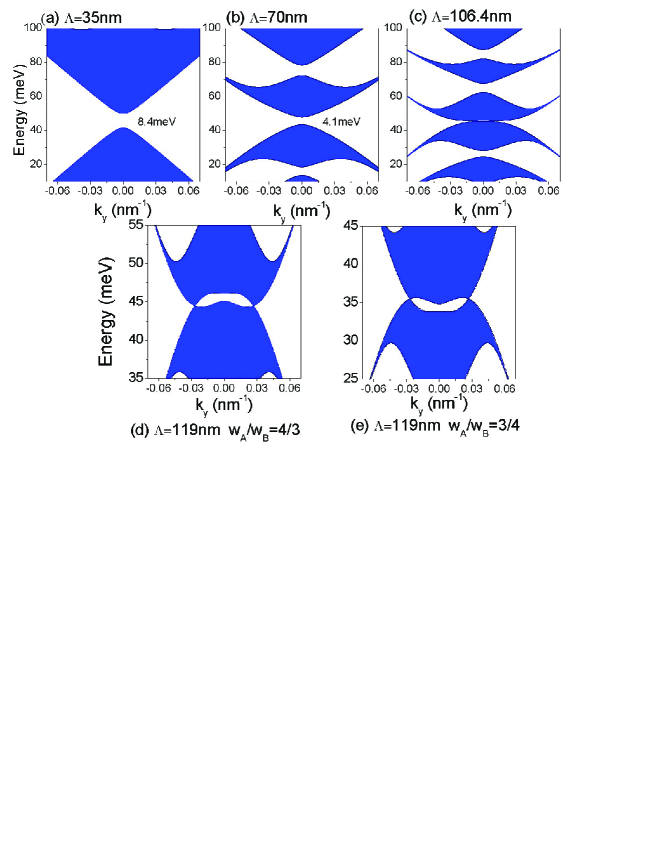
Similarly, figure 3 shows the change of the electronic band structure for the gapped graphene superlattices with unequal barrier and well widths (i.e., the ratio ). From Figs. 3(a) to 3(c), it is clear that the position of zero- gap is still independent of the lattice constant, and in this example it is located at meV, i. e., the one of roots for the condition (22) or (23). By the way, another root of the condition (22) or (23) is unphysical since it is outside of the interval . Meanwhile, the width of this zero- gap could be still adjusted by changing its lattice constant with the fixed ratio . However for the other upper and lower band gaps are strongly shifted due to the change of the lattice constant. In Fig. 3(c), it is also occurring the touching effect of the upper and lower bands due to that the condition (24) is satisfied at . Different from the above case with equal barrier and well widths (), in Fig. 3(d), when the lattice constant increases larger, the touch points move down for the inclined incidence () in the cases with . In the cases with , one can find that the touching points move up for the inclined incidence [see Fig. 3(e)]. This property of the touch points, depending on the ratio of widths , is similar to that in the gapless graphene superlattices Barbier2010 . It should be pointed out that the touch effects in Figs. 2(c) and 3(c) is very similar to the cases of zero-width band gap associated with the zero-averaged refractive index in photonic crystals containing left-handed materials LGWang2010b ; DiosLeyva2009 .
III.2 Finite periodic-barrier systems
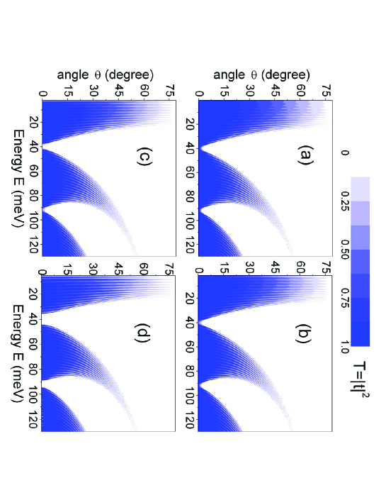
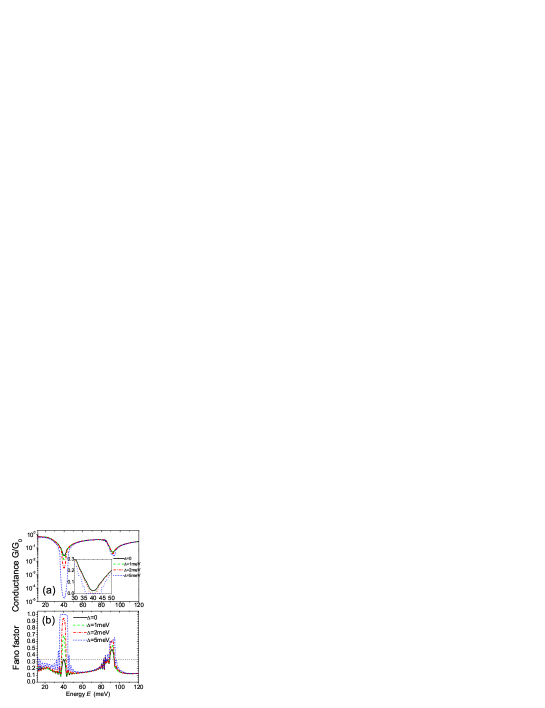
Now let us turn to discuss the properties of the transmission, conductance and Fano factor in the finite periodic-barrier systems. In order to know the information of the band structures for the finite systems, we have to calculate the transmission as functions of the incident electron energy and the incident angle. Figure 4 shows the transmission properties of an electron passing through under different values of . Figures 5(a) and 5(b) show the changes of electronic conductance and Fano factor for those cases corresponding to different situations in Fig. 4. It is clear seen that when , the electronic transmission at normal incidence is always equal to unit, see Fig. 4(a). This property is a reflection of ”Klein tunneling” in the systems of gapless graphene superlattices Barbier2008 ; Barbier2009 ; Barbier2010 ; LGWang2010 ; Arovas2010 . From Fig. 4(a), one can also find that there is a band gap opening up at all inclined angles around the energy of meV. Actually this gap is already termed as the zero- gap, which is associated with the new Dirac point, in our previous study on the gapless graphene superlattices LGWang2010 . In Fig. 5(a) and 5(b), the conductance is largest and the Fano factor is equal to 1/3 at the new Dirac point (meV) for the case of , which recovers the result for the diffusive behavior near the new Dirac point. With the increasing of , this band gap gradually opens up at the normal incidence, see Figs. 4(b)-4(d). Therefore the conductance becomes smaller and smaller when the gap is open at the normal incidence, and the Fano factor is enhanced to be larger than 1/3. From Fig. 5(a) and 5(b), one can see that when the gap is completely open for the larger value of , the Fano factor is close to unit because there is no allowed states for the electrons in this zero- gap. Another remarkable property is that near the edges of the zero- gap the Fano factor is also larger than 1/3 for the larger value of , which does not happen in the cases for smaller values of . It means that for the gapped graphene superlattices the electron’s transport has a distinct difference from the cases of gapless graphene superlattices. It should also be pointed out that the differences for the conductances of the higher band gaps in Fig. 5(a) are much small due to that the passing band is highly shifted to the higher energy for the inclined incident angles [see Figs 4(a) to 4(d)], and the Fano factor for the higher band gap in Fig. 5(b) is larger than 1/3 even for the case of .
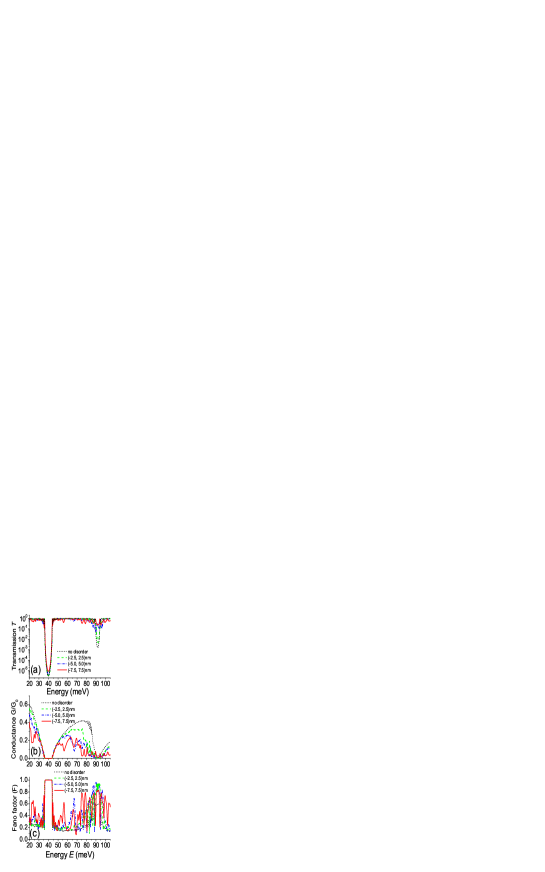
At last, we consider the effect of the structural disorder on the transmission of an electron passing through a finite gapped graphene-based periodic-barrier structure with the width deviation. Here we consider the periodic-barrier structure , as an example, with meV and nm, where is a random number. Figure 6 shows the effect of the structural disorder on electronic transmitivities, conductances and Fano factors. It is clear seen that the zero- gap is insensitive to the structural disorder, while the other band gaps are destroyed by strong disorder, see Fig. 6(a). The robustness of the zero- gap comes from the fact that the zero- solution remains invariant under disorder that is symmetric ( and equally probable), see Eq. (20). These results are very similar to that cases in the gapless graphene superlattices LGWang2010 , and the unique difference is that at the normal incidence the zero- gap is close for the gapless case while it is still open for the gapped case. From Figs. 6(b) and 6(c), one can find that the structural disorder does strongly affect on the properties of the electronic conductance and Fano factor when the incident electron’s energy is far away from the zero- gap. In Figs. 5(b,c), it is clear that the curves of the conductances and Fano factors are much different from each other for those energies far away from meV. Therefore, the zero- gap and its related properties are very insensitive to the structural disorder while the other bands and gaps are highly affected by the structural disorder.
IV Conclusions
In summary, we have studied the electronic band structures and its transport properties for the gapped graphene superlattices consisted of 1D periodic potentials of square barriers. We have found that there is a zero- gap inside the gapped graphene-based superlattices, and the location of the zero- gap is independent of the lattice constant but depends on the ratio of the barrier and well widths. Furthermore we have shown that the width of the zero- gap could be controllable by changing the lattice constant of the gapped superlattices, and under the certain condition the zero- gap could be close at the case of normal incidence and the band-crossing phenomena (the extra new Dirac points) occurs at the case of inclined incidence inside the gapped graphene superlattices, which are similar to the cases of the gapless graphene superlattices Barbier2010 ; LGWang2010 . Finally it is revealed that the properties of the electronic transmission, conductance and Fano factor near the zero- gap are insensitive to the structural disorder inside the finite periodic-barrier systems. Our analytical and numerical results on the electronic band structures and their related properties of the gapped graphene-based superlattices are hopefully of benefit to more potential applications of graphene-based devices.
Acknowledgements.
This work is supported by the National Natural Science Foundation of China (10604047 and 60806041), Hong Kong RGC Grant No. 403609 and CUHK 2060360, the Shanghai Rising-Star Program (No. 08QA14030), the Science and Technology Commission of Shanghai Municipal (No. 08JC14097), and the Shanghai Leading Academic Discipline Program (No. S30105). X. C. also acknowledges Juan de la Cierva Programme, IT 472-10, and FIS2009-12773-C02-01.References
- (1) K. S. Novoselov, A. K. Geim, S. V. Morozov, D. Jiang, Y. Zhang, S. V. Dubonos, I. V. Grigorieva, and A. A. Firsov, Science, 306, 666(2004).
- (2) Y. Zhang, Y. W. Tan, H. L. Stormer, and P. Kim, Nature (London) 438, 201 (2005).
- (3) K. S. Novoselov, A. K. Geim, S. V. Morozov, D. Jiang, M. I. Katsnelson, I. V. Grigorieva, S. V. Dubonos and A. A. Firsov, Nature 438, 197-200 (2005).
- (4) C. Berger, Z. Song, X. Li, X. Wu, N. Brown, C. Naud, D. Mayou, T. Li, J. Hass, A. N. Marchenkov, E. H. Conrad, P. N. First, W. A. de Heer, Science 312, 1191-1196 (2006).
- (5) M. I. Katsnelson, K. S. Novoselov and A. K. Geim, Nature Phys. 2, 620 (2006).
- (6) For recent reviews, see A. K. Geim, and K. S. Novoselov, Nature Mater. 6, 183-191 (2007); C. W. J. Beenakker, Rev. Mod. Phys. 80, 1337 (2008); A. H. Castro Neto, F. Guinea, N. M. R. Peres, K. S. Novoselov, and A. K. Geim, Rev. Mod. Phys. 81, 109 (2009); J. M. Pereira, F. M. Peeters, A. Chaves, G. A. Farias, Semiconductor Science and Technology 25, 033002 (2010).
- (7) M. I. Katsnelson, Zetterbewegung, chirality, and minimal conductivity in graphene, European Physical Journal B 51, 157-160 (2006).
- (8) F. Miao, S. Wijeratne, Y. Zhang, U. C. Coskun, W. Bao, C. N. Lau, Phase-Coherent transport in graphene quantum billiards, Science 317, 1530-1533 (2007).
- (9) X. Du, I. Skachko, A. Barker, and E. Y. Andrei, Nature Nanotechnology 3, 491-495 (2008).
- (10) V. V. Cheianov and V. I. Fal’ko, Phys. Rev. B 74, 041403 (2006).
- (11) A. H. Castro Neto, F. Guinea, and N. M. R. Peres, Edge and surface states in the quantum Hall effect in graphene, Phys. Rev. B 73, 205408 (2006).
- (12) M. S. Purewal, Y. Zhang, and P. Kim, Phys. Status Solidi B 243, 3418 (2006).
- (13) H. B. Heersche, P. Jarillo-Herrero, J. B. Oostinga, L. M. K. Vandersypen, A. F. Morpurgo, Nature 446, 56-59 (2007).
- (14) A. B. Kuzmenko, E. van Heumen, F. Carbone, and D. van der Marel, Phys. Rev. Lett. 100, 117401 (2008).
- (15) F. Wang, Y. Zhang, C. Tian, C. Girit, A. Zettl, M. Crommie, and Y. R. Shen, Science 320, 206 (2008).
- (16) Y. W. Son, M. L. Cohen, and S. G. Louie, Phys. Rev. Lett 97, 216803 (2006).
- (17) Y. W. Son, M. L. Cohen, and S. G. Louie, Nature 444, 347 (2006).
- (18) M. Y. Han, B. Özyilmaz, Y. Zhang, and P. Kim, Phys. Rev. Lett 98, 206805 (2007).
- (19) B. Trauzettel, D. V. Bulaev, D. Loss and Guido Burkard, Nat. Phys. 3, 192 - 196 (2007); L. A. Ponomarenko, F. Schedin, M. I. Katsnelson, R. Yang, E. W. Hill, K. S. Novoselov, A. K. Geim, Science 320, 356 (2008); F. Libisch, C. Stampfer, and J. Burgdörfer, Phys. Rev. B 79, 115423 (2009).
- (20) C. L. Kane and E. J. Mele, Phys. Rev. Lett. 95, 226801 (2005).
- (21) H. Min, J. E. Hill, N. A. Sinitsyn, B. R. Sahu, L. Kleinman, and A. H. MacDonald, Phys. Rev. B 74, 165310 (2006).
- (22) Y. Yao, F. Ye, X. L. Qi, S. C. Zhang, and Z. Fang, Phys. Rev. B 75, 041401(R) (2007).
- (23) G. Giovannetti, P. A. Khomyakov, G. Brocks, P. J. Kelly, and J. van den Brink, Phys. Rev. B 76, 073103 (2007).
- (24) S. Y. Zhou, G. -H. Gweon, A. V. Fedorov, P. N. First, W. A. De Heer, D. -H. Lee, F. Guinea, A. H. Castro Neto, and A. Lanzara, Nature Materials 6, 770 (2007).
- (25) S. Kim, J. Ihm, H. J. Choi, and Y. W. Son, Phys. Rev. Lett. 100, 176802 (2008).
- (26) A. Qaiumzadeh and R. Asgari, New Journal of Physics 11, 095023 (2009).
- (27) E. J. Duplock, M. Scheffler, and P. J. D. Lindan, Phys. Rev. Lett. 92, 225502 (2004); L. A. Chernozatonskiĭ, P. B. Sorokin, E. E. Belova, J. Brüning and A. S. Fedorov, JETP Lett. 85, 77 (2007); J. O. Sofo, A. S. Chaudhari, and G. D. Barber, Phys. Rev. B 75, 153401 (2007); T. G. Pedersen, C. Flindt, J. Pedersen, N. A. Mortensen, A.-P. Jauho, and K. Pedersen, Phys. Rev. Lett. 100, 136804 (2008).
- (28) R. Balog, B. Jørgensen, L. Nilsson, M. Andersen, E. Rienks, M. Bianchi, M. Fanetti, E. Lægsgaard, A. Baraldi, S. Lizzit, Z. Sljivancanin, F. Besenbacher, B. Hammer, T. G. Pedersen, P. Hofmann, and L. Hornekær, Nat. Materials 9, 315-319 (2010).
- (29) R. Tsu, Superlattice to Nanoelectronics (Elsevier, Oxford, 2005).
- (30) C. Bai and X. Zhang, Phys. Rev. B 76, 075430 (2007).
- (31) C. -H. Park, L. Yang, Y.-W. Son, M. L. Cohen, and S. G. Louie, Nature Phys. 4, 213 (2008).
- (32) M. Barbier, F. M. Peeters, P. Vasilopoulos, and J. M. Pereira, Jr., Phys. Rev. B 77, 115446 (2008).
- (33) C.-H. Park, L. Yang, Y.-W. Son, M. L. Cohen, and S. G. Louie, Phys. Rev. Lett. 101, 126804 (2008).
- (34) M. Barbier, P. Vasilopoulos, and F. M. Peeters, Phys. Rev. B 80, 205415 (2009).
- (35) R. P. Tiwari and D. Stroud, Phys. Rev. B. 79, 205435 (2009).
- (36) M. Ramezani Masir, P. Vasilopoulos, A. Matulis, and F. M. Peeters, Phys. Rev. B 77, 235443 (2008); M. Ramezani Masir, P. Vasilopoulos, and F. M. Peeters, Phys. Rev. B 79, 035409 (2009); L. Dell’Anna and A. De Martino, Phys. Rev. B 79, 045420 (2009); L. Dell’Anna1 and A. De Martino, Phys. Rev. B 80, 155416 (2009); S. Ghosh and M. Sharma, J. Phys. Condens. Matter 21, 292204 (2009).
- (37) L. Brey and H. A. Fertig, Phys. Rev. Lett. 103, 046809 (2009).
- (38) C. H. Park, Y. W. Son, L. Yang, M. L. Cohen, and S. G. Louie, Phys. Rev. Lett. 103, 046808 (2009).
- (39) M. Barbier, P. Vasilopoulos, and F. M. Peeters, Phys. Rev. B. 81, 075438 (2010).
- (40) L. G. Wang and S. Y. Zhu, Phys. Rev. B 81, 205444 (2010).
- (41) D. P. Arovas, L. Brey, H. A. Fertig, E.-A. Kim, and K. Ziegler, arXiv:1002.3655V2 (2010).
- (42) J. H. Ho, Y. H. Chiu, S. J. Tsai, and M. F. Lin, Phys. Rev. B 79, 115427 (2009).
- (43) J. V. Gomes and N. M. R. Peres, J. Phys.: Condens. Matter 20, 325221 (2008).
- (44) B. Soodchomshom, I.-M. Tang, R. Hoonsawat, Phys. Lett. A 373, 3477 (2009).
- (45) L. Jiang, Y. Zheng, H. Li, and H. Shen, Nanotechnology 21, 145703 (2010).
- (46) M. Esmailpour, A. Esmailpour, R. Asgari, M. Elahi, M. R. Rahiimi Tabar, Solid State Communications 150, 655 (2010).
- (47) F. Guinea, T. Low, arXiV:1006.0127 (2010).
- (48) J. Li, L. Zhou, C. T. Chan, and P. Sheng, Phys. Rev. Lett. 90, 083901 (2003).
- (49) A. Qaiumzadeh and R. Asgari, Phys. Rev. B 79, 075414 (2009).
- (50) V. V. Cheianov, V. Fal’ko, and B. L. Altshuler, Science 315, 1252 (2007).
- (51) S. Datta, Electronic Transport in Mesoscopic Systems, Cambridge University Press, 1995.
- (52) J. Tworzydlo, B. Trauzettel, M. Titov, A. Rycerz, and C. W. J. Beenakker, Phys. Rev. Lett. 96, 246802 (2006).
- (53) L. G. Wang and S. Y. Zhu, Appl. Phys. B 98, 459 (2010).
- (54) M. de Dios-Leyva and J. C. Drake-Pérez, Phys. Rev. E 79, 036608 (2009).
Figures Captions:
Fig. 1. (Color online). (a) Schematic of a gapped graphene superlattice with periodic electrodes. (b) Schematic diagram of the electronic spectrum of the gapped graphene superlattice, and the pink dotted line denotes the periodic potentials of squared barriers.
Fig. 2. (Color online). Electronic band structures for the gapped graphene superlattices with equal barrier and well widths (): (a) nm, (b) nm, (c) nm, and (d) nm; and dependence of the band-gap structure on the lattice constant with a fixed transversal wave number: (e) and (f) nm-1. The other parameters are meV, meV and .
Fig. 3. (Color online). Electronic band structures for the gapped graphene superlattices with unequal barrier and well widths (): (a) nm, (b) nm, (c) nm, and (d) nm; and (e) electronic band structures for the case of and nm. The other parameters are the same as in Fig. 2.
Fig. 4. (Color online). Effects of the parameter on the electronic transmission for the finite structure , (a) , (b) meV, (c) meV, and (d) meV. The other parameters are nm, , meV, and .
Fig. 5. (Color online). The effects of the parameter on (a) conductance and (b) Fano factor. The other parameters are the same as in Fig. 4.
Fig. 6. (Color online). The effect of the structural disorder on (a) electronic transimitivity , (b) conductance , and (c) Fano factor, for the gapped graphene superlattice with meV, meV and and nm, where is a random number. The short-dashed lines denote for the structure without disorder, the dashed lines for nm, the dashed-dot lines for nm, and the solid lines for nm.