Tunneling Conductance of The Graphene SNS Junction with a Single Localized Defect
Abstract
We study the electronic transport in a graphene-based superconductor-normal(graphene)-superconductor (SNS) junction by use of the Dirac-Bogoliubov-de Gennes equation. We consider the properties of tunneling conductance through an undoped strip of graphene with heavily doped superconducting electrodes in the dirty limit . We find that spectrum of Andreev bound states are modified in the presence of single localized defect in the bulk. The minimum tunneling conductance remains the same and this result doesn’t depend on the actual location of the imperfection.
pacs:
74.45.+c, 74.50.+r, 73.23.Ad, 74.78.NaI Introduction
Graphene, namely a monolayer of graphite, is formed by carbon atoms on a two-dimensional honeycomb lattice. In graphene, due to its unique band structure whose valence and conductance bands touch at two inequivalent Dirac points (often referred to as and ) of the Brillouin zone, the electrons around the Fermi level obey the massless relativistic Dirac equation which results in the linear energy dispersion relation. Recent exciting developments in transport experiments on graphene has stimulated theoretical studies of superconductivity phenomena in this material, which has been recently fabricated Nov-1 ; Zhan-1 . A number of unusual features of superconducting state have been predicted, which are closely related to the Dirac-like spectrum of normal state excitationBen-A ; Lee-1 . In particular, the unconventional normal electron dispertion has been shown to result in a nontrivial modification of Andreev reflection and Andreev bound states in Josephson junctions with supercomducting graphene electrodesMai-1 ; Ash-1 ; Bol-1 .
Other interesting consequences of the existence of Dirac-like quasiparticles can be understood by studying superconductivity in grapheneMou-1 ; Khv-1 ; Ale-1 ; Mor-1 ; Fog-1 . It has been suggested that superconductivity can be induced in graphene layer in the presence of a superconducting electrode near it via proximity effect Ben-1 ; Volk-1 ; Tit-1 .
In this work, we study Josephson effect and find bound state in graphene for tunneling SNS junction with the presence of a single localized defectMou-2 . In this study, we shall concentrate on SNS junction with normal region thickness , where is the superconducting coherence length, and width which has an applied gate voltage across the normal regionMou-3 ; Sal-1 . In the frame of the dirty limit cosidered by Kulik and Omelyanchuk we investigate tunneling condactance in SNS junction with presense a single localized defect and find that Andreev levels are modified, the minimum tunneling conductance remains the sameKul-1 ; And-1 ; Le-1 .
II Tunneling conductance of the graphene superconductor/normal/superconductor junction with a single localized defect
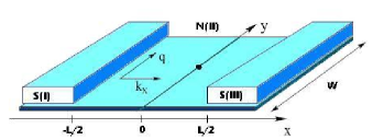
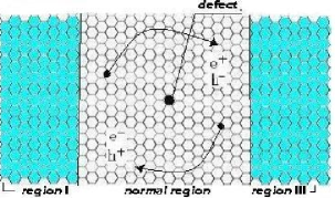
We consider a SNS junction with a single localized defect which is involved in a graphene sheet of width lying in the plane extends from to while the superconducting region occupies (see Fig. 1). The SNS junction can then be described by the Dirac-Bogoliubov-de-Gennes (DBdG) equationsBen-2 ,
Here , , are the component wave functions for the electron and hole spinors, the index denote or for electrons or holes near and points, takes values for , denotes the Fermi energi, and denote the two inequivalent sites in the hexagonal lattice of graphene, and the Hamiltonian is given by
| (1) |
In Eq. 1, denotes the Fermi velocity of the quasiparticles in graphene and takes values for . The Pauli matrices act on the sublattice index. The excitation energy is measured relative to the Fermi level(set at zero). The electrostatic potential and pair patential have step function profiles, as in the case of a semiconductor two-dimensional electron gas Volk-2 ; Fag-1 ; Gla-1 ,
The reduction of the order parameter in the superconducting region on approaching the SN interface is neglected; i.e., we approximate parameter as we’ve done it above. As discussed by Likharev Lik-1 , this approximation is justified if the weak link has length and width much smaller than . There is no lattice mismatch at the NS interface, so the honeycomb lattice of graphene is unperturbed at the boundary, the interface is smooth and impurity free.
Solving the DBdG equations, we gain the wave-functions in the superconducting and the normal regions. In region , for the DBdG quasiparticles moving along the direction with a transverse momentum and energy , the wave-functions are given by
The parameters , , , are defined by , , , and denotes region , for and for correspondently. Further we assumed that the Fermi wave length in the superconducting region much smaller than the wave length in the normal region and . Since , this regime of a heavely doped superconductor corresponds to the limits , , .
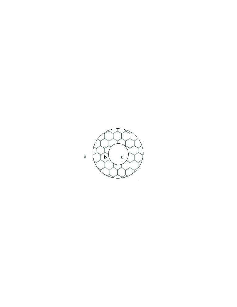
The region consists of three areas: (see Fig. 2). We solve the DBdG equations for the area , while area is the area where placed defect and area would be extended and matched with superconducting regions. The two valleys decouple, and we can solve equations separately for each valley, , . The term proportional to in Hamiltonian is a mass term confining the Dirac electrons in the area . Rewrite the Hamiltonian in the cylindrical coordinates and since commutes with , its electron-eigenspinors are eigenstates of Ben-ring ,
with eigenvalues , where is a half-odd integer, and is the Bessel function of order. In the plane denotes moving direction of correspondent quasiparticle, for the quasiparticle moving toward and for the quasiparticle moving toward direction correspondentely. Further we are interested in to find zero energy statesTit-1 . In this case the DBdG equations posses a general symmetry with respect to the change in the sign of energy
| (2) |
where we denote and . Thus, for a set of zero modes (,) enumerated by a certain index we should have,
| (3) |
In the same manner as for electron hole-spinors have form
with the definitions
| (4) |
| (5) |
The angle is the angle of incidence of the electron (having longitudinal wave vector ), and is the reflection angle of the hole (having longitudinal wave vector ) Asa-1 ; Bhat-1 . To obtain an analytical approximation of the spectrum, we use the asymptotic form of the Bessel functions for large . This indeed is the desired limit as , where is the defect radius (the radius of the area ) and determine for all eigenvalues . In this limit we impose the infinite mass boundary conditions at , for which in the area with in the and areas consequently . Half-odd integer values reflect the Berry’s phase of closed size of a single localized defect in graphene.
To obtain the subgap () Andreev bound states, we now impose the boundary conditions at the graphene. The wave-functions in the superconducting and normal regions can be constructed as
| (6) | |||
| (7) |
where are the amplitudes of right and left moving DBdG quasiparticles in region and and are the amplitudes of right(left) moving electrons and holes, respectively, in the normal regionMai-1 . These wave functions must satisfy the boundary conditions,
| (8) |
Since the wave vector parallel to the interface and different wave vectors in the -direction are not coupled, we may solve the problem for a given and we can consider each transverse mode separately. To leading order in the small parameter we may substitute , . After some algebra we obtain equation
| (9) |
Eq. 9 differs from equation obtained for SNS junction without a single defect. Eliminating second term in Eq. 9 we could immediately yield reduction of the equation and it earns a essential form for weak SNS junctionsTit-1 . The solution of Eq. 9 is a single bound state per mode,
| (10) |
where
| (11) |
| (12) |
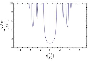
We don’t have a simple analytic expression for the -dependance but we obtained modified Andreev levels with the presense a single localized defect in the bulk. The conductance of the graphene strip is expressed through the transmission probability by the Landauer formula,
| (13) |
where is given by =Int. Substitution transmission probability into Eq. 13 gives the conductance versus Fermi energy (see in Fig. 3,Fig. 4). The result for the minimal conductivity agrees with other calculationsLud ; Zi ; Per , which start from an un- bounded disordered system and then take the limit of infinite mean free path . There is no geometry dependence if the limits are taken in that order.
III Summary
In the conclusion, we have shown that tunneling conductance of the graphene SNS junction with a single localized defect has a nonzero minimal value if the Fermi level is tuned to the point of zero carrier concentration.We have demonstrated that the tunneling conductance exhibits oscillatory behavior. Andreev levels are modified, the minimum tunneling conductance remains the same and this result doesn’t depend on the actual location of the imperfection. The consideration of tunneling conductance of SNS junctions with multiple defects is the subject of forthcoming article.
IV Acknowledgments
Authors are very indebted to Prof. H.H. Lin for stimulating discussions and thank anonymous referees for valuable and credible comments. We acknowledge support from the National Center for Theoretical Sciences in Taiwan.
References
- (1) K.S. Novoselov, A.K. Geim, S.V. Morozov, D. Jiang, M.I. Katsnelson, I.V. Grigorieva, S.V. Dubonos, and A.A. Firsov, Nature 438, 197 (2005).
- (2) Y. Zhang, Y.-W. Tan, H.L. Stormer, and P.Kim, Nature 438, 201 (2005).
- (3) W. J. Beenakker and H. van Houten, Phys. Rev. Lett. 66, 3056 (1991).
- (4) Q.-H. Wang and D.-H. Lee, Phys. Rev. B 67, 20511 (2003).
- (5) M. Maiti and K. Sengupta, Phys. Rev. B 76, 054513 (2007).
- (6) P. Ghaemi, Fa Wang, and Ashvin Vishwanath, Phys. Rev. Lett. 102, 157002 (2009).
- (7) Dima Bolmatov, Chung-Yu Mou, Physica B: Condensed Matter 405, 2896-2899 (2010).
- (8) H.H. Lin, T. Hikihara, H.T. Jeng, B.L. Huang, and C.Y. Mou, X. Hu, Phys. Rev. B 79, 035405 (2009).
- (9) D.V. Khveshchenko, J. Phys.: Condens. Matter 21, 075303 (2009).
- (10) I.L. Aleiner, D.E. Kharzeev, and A.M. Tsvelik, Phys. Rev. B 76, 195415 (2007).
- (11) A.F. Morpurgo, F. Guinea, Phys. Rev. Lett. 97, 196804 (2006).
- (12) M.M. Fogler, D.S. Novikov, and B.I. Shklovskii, Phys. Rev B 76, 233402 (2007).
- (13) C.V.J. Beenakker , Phys. Rev. Lett. 97, 067007 (2006).
- (14) A.F. Volkov, P.H.C. Magnee, B.J. van Wees, and T.M. Klapwijk, Physica C 242, 261 (1995).
- (15) M. Titov and C.W.J. Beenakker, Phys. Rev. B 74, 041401(R)(2006).
- (16) B.L. Huang, C.Y. Mou, EPL 88, 68005 (2009); D. Bolmatov, Chung-Yu Mou, JETP 110, 612-616 (2010).
- (17) S.T. Wu and C.Y. Mou, Phys. Rev. B 67, 024503 (2003).
- (18) E. Zhao and J.A. Sauls, Phys. Rev. Lett. 98, 206601 (2007).
- (19) I.O. Kulik and A. Omelyanchuk, JETP Lett. 21, 96 (1975); Sov.Phys. JETP 41, 1071 (1975).
- (20) A.F. Andreev, Zh. Eksp. Teor. Fiz. 46, 1823 (1964).
- (21) P.A. Lee, Phys. Rev. Lett. 71, 1887 (1993).
- (22) C.W.J. Beenakker, cond-mat/0604594.
- (23) A.F. Volkov, P.H.C. Magnee, B.J. van Wees, and T.M. Klapwijk, Physica C 242, 261 (2006).
- (24) G. Fagas, G. Tkachov, A.Pfund, and K. Richter, Phys. Rev. B 71, 224510 (2005).
- (25) M.G. Vavilov, I.L. Aleiner, and L.I. Glazman, Phys. Rev. B 76, 115331 (2007).
- (26) A review of superconducting weak links is K. K. Likharev, Rev. Mod. Phys. 51, 101 (1979).
- (27) P. Recher, B. Trauzettel, A. Rycerz, Ya.M. Blanter, C.W.J. Beenakker, and A.F. Morpurgo, Phys. Rev. B 76, 235404 (2007).
- (28) Y. Asano, T. Yoshida, Y. Tanaka, and Alexander A. Golubov, Phys. Rev. B 78, 014514 (2008).
- (29) S. Bhattacharjee and K. Sengupta, Phys. Rev. Lett. 97, 217001 (2006).
- (30) A. W. W. Ludwig, M. P. A. Fisher, R. Shankar, and G.Grinstein, Phys. Rev. B 50, 7526 (1994).
- (31) K. Ziegler, Phys. Rev. Lett. 80, 3113 (1998).
- (32) N. M. R. Peres, F. Guinea, and A. H. Castro Neto, Phys. Rev. B 73, 125411 (2006).