Control of electric current by graphene edge structure engineering
Abstract
In graphene nanoribbon junctions, the nearly perfect transmission occurs in some junctions while the zero conductance dips due to anti-resonance appear in others. We have classified the appearance of zero conductance dips for all combinations of ribbon and junction edge structures. These transport properties do not attribute to the whole junction structure but the partial corner edge structure, which indicates that one can control the electric current simply by cutting a part of nanoribbon edge. The ribbon width is expected to be narrower than 10 nm in order to observe the zero conductance dips at room temperature.
pacs:
72.10.-d,72.15.Rn,73.20.At,73.20.Fz,73.23.-bGraphene is one of the most promising materials for future electronics. The electron mobility of graphene is much larger than that of silicon and the thermal mobility is twice that of diamond emob1 ; emob2 ; thmob . These properties are, however, not enough for fabricating switching devices by graphene. The electric current must be easily controlled by external gate voltage in such devices while traveling electrons in graphene are hardly stopped by potentials due to the Klein tunneling Klein ; Klein2 .
One possible way for overcoming this problem is the utilization of edge structures. In graphene, the electronic band structure of electrons is strongly affected by edge structures peculiar ; nakada ; prb . Graphene nanoribbons (GNR) with zigzag edges are known to have partial flat bands near the Fermi energy due to the edge localized states. The electronic structures of nanoribbons with armchair edges crucially depend on the ribbon width peculiar ; nakada ; prb ; son . These properties also result in peculiar transport phenomena in GNR pcc ; pcc2 ; nearlyPCC . Moreover, strong energy dependence of conductance has been predicted when two edge structures are connected at the corner junction ; ajunc .
A number of theoretical works have been done on the transport in GNR. Still, a simple classification of transport properties in GNR junctions has been lacked. Such a classification will be quite useful for fabricating nanographene devices in the future. At present, the fabrication of creating clean-edge GNR has been experimentally succeeded jia ; unzip ; unzip2 .
In this Letter, we numerically investigate the electronic transport in GNR junctions and GNR with partial edge cutting. In the single-channel energy regime, the conductance mostly remains unity in armchair edge junction while the zero conductance dips appear in zigzag one. We classify details of the zero conductance dips for all combinations of ribbon and junction edge structures.
We describe the electronic states of GNR by the tight-binding model ,
| (1) |
where denotes the creation (annihilation) operator of an -electron on the site , neglecting the spin degree of freedom. The hopping is restricted in the nearest neighboring atoms. The conductance is defined by the Landauer formula,
| (2) |
with . Here the transmission matrix can be calculated by using the recursive Green function method gf .
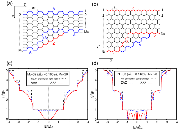
Firstly, we consider GNR junctions as shown in Fig. 1(a) and (b). Junctions are classified into the armchair ribbon with armchair edge junction (AAA-junction), that with zigzag one (AZA-junction), the zigzag ribbon with armchair edge junction (ZAZ-junction) and that with zigzag one (ZZZ-junction). The width of left (right) armchair ribbon is defined by while that of zigzag one is by . Here we note that the armchair ribbon is metallic only for while the zigzag ribbon is always metallic.
Figure 1(c) and (d) show the energy dependence of the conductance for armchair and zigzag ribbon junctions, respectively. We set and . The energy is normalized by ), denoting the end of single-channel energy regime of the left wider armchair (zigzag) ribbon. These energy scales are related to the ribbon width by and where and for armchair and zigzag ribbons, respectively. The maximum conductance is limited by the number of channel at the right narrower ribbon (black dotted line in Fig. 1(c) and (d)).
The behaviour of conductance strongly depends on junction structure in the single-channel energy regime () while it does not in the multi-channel one (). In the single-channel energy regime, the conductance mostly remains unity in the AAA-junction while the zero conductance dip appears in the AZA-junction at . This zero conductance dip is due to the anti-resonance induced by the coupling between a continuous state at ribbon and a localized state at zigzag edge junction. In addition, the junction region is mainly semiconducting and works as a barrier for low-energy transport in the AZA-junction since the ribbon width are narrowed as . Hence, by the combination of a resonance and a barrier effect, the width of zero conductance dip in the AZA-junction is rather wide and the FWHM (full width at half maximum) can be roughly estimated as . On the other hand, the junction region is always metallic or semiconducting in the AAA-junction since the ribbon width are narrowed as .
In the ZAZ-junction, the sharp zero conductance dips appear in the vicinity of the end of single-channel energy regime (). In zigzag ribbons, propagating electrons belong to one of two valleys in the single-channel energy regime while the second channel will be opened in both valleys as the energy of incident electrons increases pcc2 . Since the group velocity of a second channel is almost zero at the bottom of subband, the second channel in the other valley works as a bound state similar to the zigzag edge state at . The FWHM of dips can be roughly estimated as in our numerical simulation performed for several different values of the ribbon width and the width difference within the range .
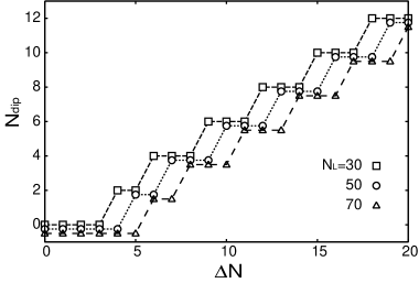
In the ZZZ-junction, several zero conductance dips appear at non-zero energies. This is due to the energy level splitting induced by the coupling between the edge-localized state on A-sublattice at ribbon and the edge-localized states on B-sublattice at junction. Moreover, the coupled states have different nodes as the width difference is getting larger junction . The number of zero conductance dips is given by where denotes the number of nodes. Figure 2 shows the number of zero conductance dips as a function of the width difference . It is shown that, except for small , is related to as , where denotes the integer part of and is the integer number depending on (for instance, as shown in Fig. 2). The position and width of each dip depends not only on but also on . We do not discuss details of them in this Letter, but the FWHM of the widest dip can be roughly estimated as in our simulation. The appearance of zero conductance dips is classified for all combinations of ribbon and junction edge structures in Table 1.
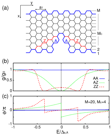
In order to obtain various zero conductance dips, it is in fact not necessary to fabricate GNR junctions. Secondly, we consider an ideal GNR with partial edge cutting as shown in Fig. 3(a). The partial edge cutting are classified into armchair-armchair (AA), armchair-zigzag (AZ) and zigzag-zigzag (ZZ). Figure 3(b) shows the conductance as a function of energy in the single-channel energy regime (). Similar to the AAA-junction, the conductance remains unity for the AA-cut although it has the sharpest hollow among three cutting patterns. On the other hand, the zero conductance dips due to anti-resonance appear for the AZ-cut and the ZZ-cut. We note that, in the ZZ-cut, the number of zero conductance dips increases as the edge-cut becomes deeper, i.e., becomes larger, as the same as the ZZZ-junction. This is not case for the AZ-cut where the zero conductance dip always appears at as the same as the AZA-junction.
In order to clarify that the zero conductance dips are originated from anti-resonance, we evaluate the phase shift of transmission coefficient as a function of energy (Fig. 3(c)). Here the phase shift is given by where denotes the transmission coefficient in the single-channel energy regime. It is known that the abrupt -phase jump occurs when the energy of incident electrons are passing through the anti-resonance levels junction . One can clearly see such -phase jumps (Fig. 3(c)) at the position of zero conductance dips (Fig. 3(b)).
Finally, we discuss the effect of temperature. At finite temperature, the conductance is given by where denotes the thermal broadening function with the Fermi distribution function . In order to observe the resonance effect clearly, the FWHM of zero conductance dips must be wider than that of , which is about . The energy width is inversely proportional to the ribbon width and one can roughly estimate that nm for K. We also note that the phase coherence is necessary in order to observe the resonance effect while it can be broken by inelastic scatterings due to the electron-phonon coupling at finite temperature. However, it is known that the effect of electron-phonon coupling is weak in carbon nanotube and the inelastic mean free path is estimated as nm at low bias 6Suzuura ; 3Javey ; 15Park . This is due to the peculiar band structure of graphene so that the same weakness is also expected in GNR.
In conclusion, we have numerically investigated the electronic transport in GNR junctions and GNR with partial edge cutting. In the single-channel energy regime, the nearly perfect transmission occurs in armchair edge junction while the perfect reflection occurs at certain energies in zigzag one. The appearance of zero conductance dips (perfect reflection) is due to the anti-resonance between a continuous state at ribbon and an localized state at zigzag-edge junction, which can be verified by evaluating the phase shift of an transmission coefficient. We have classified the number, position and width of these zero conductance dips for all combinations of ribbon and junction edge structures. Since these low-energy transport properties do not attribute to the whole junction structure but the partial corner edge structure, one can control the electric current simply by cutting a part of GNR edge. Although the ribbon width must be as narrow as 10 nm in order to observe this resonance effect at room temperature, the effect should be detectable at low temperature experiment once the technique of fabricating smooth graphene edges is well established.
This work was financially supported by a Grand-in-Aid for Scientific Research from the MEXT and the JSPS (Nos. 19710082, 19310094 and 20001006).
| Ribbon | Junction | Zero conductance dips | ||
| Number | Position | Width (FWHM) | ||
| A | A | 0 | —– | —– |
| Z | 1 | |||
| Z | A | 2 | ||
| Z | 2 Int | * | ||
| for the widest dip | ||||
| A: armchiar, Z:zigzag, *: not discussed in this letter | ||||
References
- (1) S.V. Morozov, K.S. Novoselov, M.I. Katsnelson, F. Schedin, D.C. Elias, J.A. Jaszczak and A.K. Geim, Phys. Rev. Lett. 100, 016602 (2008).
- (2) K.I. Bolotin, K.J. Sikes, Z. Jiang, M. Klima, G. Fudenberg, J. Hone, P. Kim and H.L. Stormer, Sol. Stat. Comm. 146, 351 (2008).
- (3) A.A. Balandin, S. Ghosh, W. Bao, I. Calizo, D. Teweldebrahn, F. Miao and C.N. Lau, Nano Lett. 8, 902 (2008).
- (4) M.I. Katsnelson, K.S. Novoselov and A.K. Geim, Nature Phys. 2, 620 (2006).
- (5) A.F. Young and P. Kim, Nature Phys. 5, 222 (2009).
- (6) M. Fujita, K. Wakabayashi, K. Nakada and K. Kusakabe, J. Phys. Soc. Jpn. 65, 1920 (1996).
- (7) K. Nakada, M. Fujita, G. Dresselhaus and M.S. Dresselhaus, Phys. Rev. B 54, 17954 (1996).
- (8) K. Wakabayashi, M. Fujita, H. Ajiki and M. Sigrist, Phys. Rev. B 59, 8271 (1999).
- (9) Y.-W. Son, M.L. Cohen and S.G. Louie, Phys. Rev. Lett. 97, 216803 (2006).
- (10) K. Wakabayashi, Y. Takane and M. Sigrist, Phys. Rev. Lett. 99, 036601 (2007).
- (11) K. Wakabayashi, Y. Takane, M. Yamamoto and M. Sigrist, CARBON 47, 124 (2009).
- (12) M. Yamamoto, Y. Takane and K. Wakabayashi, Phys. Rev. B 79, 125421 (2009).
- (13) K. Wakabayashi, Phys. Rev. B 64, 125428 (2001).
- (14) H. Li, L. Wang and Y. Zheng, J. Appl. Phys. 105, 013703 (2009).
- (15) X. Jia, M. Hofmann, V. Meunier, B.G. Sumpter, J.Campos-Delgado, J.M. Rome-Herrera, H. Son, Y.-P. Hsieh, A. Reina, J. Kong, M. Terrones and M.S. Dresselhaus, Science 323, 1701 (2009).
- (16) D.V. Kosynkin, A.L. Higginbotham, A. Sinitskii, J.R. Lomeda, A. Dimiev, B.K. Price and J.M. Tour, Nature 458, 872 (2009).
- (17) L. Jiao, L. Zhang, X. Wang, G. Diankov and H. Dai, Nature 458, 877 (2009).
- (18) T. Ando, Phys. Rev. B 44, 8017 (1991).
- (19) H. Suzuura and T. Ando, Phys. Rev. B 65, 235412 (2002).
- (20) A. Javey, J. Guo, M. Paulsson, Q. Wang, D. Mann, M. Lundstrom and H. Dai, Phys. Rev. Lett. 92, 106804 (2004).
- (21) J.-Y. Park, S. Rosenblatt, Y. Yaish, V. Sazonova, H. Üstünel, S. Braig, T.A. Arias, P.W. Brouwer and P.L. McEuen, Nano Lett. 4, 517 (2004).