Lifetime measurements () of electron spins in Si/SiGe quantum dots
Abstract
We have observed the Zeeman-split excited state of a spin- multi-electron Si/SiGe depletion quantum dot and measured its spin relaxation time in magnetic fields up to T. Using a new step-and-reach technique, we have experimentally verified the -value of for the observed Zeeman doublet. We have also measured of single- and multi-electron spins in InGaAs quantum dots. The lifetimes of the Si/SiGe system are appreciably longer than those for InGaAs dots for comparable magnetic field strengths, but both approach one second at sufficiently low fields ( T for Si, and T for InGaAs).
Introduction Gate-defined quantum dots (QD) in the Si/SiGe material system have been touted as one of the more promising candidates for spin-based quantum computation, primarily because of the long decoherence time expected for electron spins in Si Ericksson . Because establishes a natural upper bound on , a measurement of the spin relaxation time for isolated electrons in any Si-based system has been an important and actively-pursued objective Si-based ; Simmons . Although there has been significant progress in fabricating and testing few-electron Si/SiGe dots Simmons , there has been, up until now, no direct measurement showing the anticipated long spin-relaxation lifetimes. Indeed, there has been no direct measurement of a Zeeman splitting for either single- or few-electron states in any Si-based quantum dot.
In this Letter, we report the first direct experimental confirmation of a Zeeman spin excited state in a few-electron Si/SiGe quantum dot, and a measurement of its lifetime as a function of magnetic field. We also report comparable data for InGaAs dots, used as a testbed for our measurement techniques. These dots could be emptied, thus allowing us to measure single-electron spins.
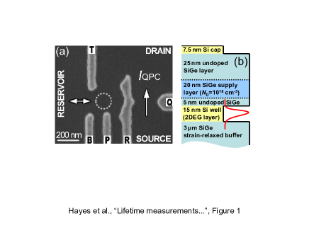
Dot Particulars Figure 1 shows the electrode layout and epitaxial structure for our Si/Si0.7Ge0.3 dot. The InGaAs/InAlAs/InP depletion dot had an almost identical electrode geometry, but a different epitaxial structure which incorporated two quantum wells, not one, so that the wafer could also be used for accumulation-mode devices (described elsewhere Croke ). In our depletion-mode devices, the upper well in the InGaAs structure played no role.
Measurement The dot was electrostatically formed using conventional techniques Elzerman . We found, empirically, that the lowest number of electrons on the dot, , can be reached when the T–R channel is pinched off and the T–B channel kept open. However, as the electrode voltages are lowered to drive additional electrons off the dot, the T–B channel eventually becomes pinched off also, preventing any further reduction in N. Although we routinely reached in InGaAs dots before this happened, the lowest value of obtained for Si/SiGe dots was likely , and this only after several painstaking redesigns of the electrodes in which the gaps for the T–B and T–R channels were progressively widened.
When was reached, was measured by repeatedly applying a three-step bias sequence to one of the electrodes (a technique first used in Elzerman2 ). The response of the charge-monitoring currrent, , to the bias changes is twofold: (i) a drop in the current by a fixed amount when an electron is (spontaneously) added to the dot, and an increase when it is removed, as shown by the dashed lines in Figure 2, and (ii) a replication of the bias sequence due to unwanted capacitive coupling of the driven electrode to the R–Q channel.
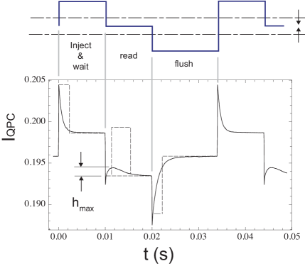
The key response is the rectangular pulse formed during the read interval, which only forms when a loaded excited-state electron does not decay to the ground state during the wait-time. A time-average of this rectangular pulse gives a “spin bump” having the analytic form
where () is the tunneling time off of (onto) the dot, and is the fraction of electrons that load into the excited state during the inject pulse and survive the wait-time without decaying to the ground state. For equal tunneling times this expression reduces to .
With increasing wait-time , the fraction of instances when an unload-reload pulse is formed during the read interval will decay exponentially as (assuming that the characteristic time ). The spin bump height , plotted versus , will show the same exponential decay, as demonstrated by the data in Fig. 3.
There are two advantages of using time-averaging rather than the pulse-counting of Elzerman2 : (i) the high signal-to-noise ratio required to reliably detect individual pulses is not needed, and (ii) the false counts due to random telegraph signals (RTS) that will unavoidably occur when the read level is near the lower Zeeman level contribute trivially, because the average of RTS-induced pulses is a straight line. What is lost by using the averaging approach is a direct measure of the branching ratio, . However, is not needed for a determination of .

Zeeman splitting The spin-bump appears when, and only when, the amplitude of the inject-and-wait pulse is sufficient to reach the first excited state. This suggests a step-and-reach technique for measuring the Zeeman splitting. One places the read level a known amount above the ground state (the step process), and then progressively reaches up with the inject pulse until a bump appears. The exact point of appearance of the bump is determined experimentally by measuring the bump height for several values of step-plus-reach amplitude just beyond the first appearance of the bump, and then extrapolating backward to determine the zero-intercept. To convert the combined step and reach amplitudes to an actual energy, we used a temperature sweep and the known relation between the width of a Coulomb Blockade peak and the dot’s temperature Meirav to determine both the lever arm, , and the effective base temperature of the system, /eV and mK, respectively.
The Zeeman splitting was measured for several values of the magnetic field using this technique. Two sets of measurements were made, one with the magnetic field increasing with each successive point, the other with it decreasing, in order to look for hysteretic effects (which we did not see). These data are plotted in Fig. 4. One sees immediately that there is a small but non-negligible deviation from a straight line at higher values of , which we suspect may be caused by a small component of the magnetic field normal to the 2DEG. We have fit the measured points to the somewhat arbitrary function , using values of ranging from to infinity, and have found that these fits give a zero-field value of that ranges from to . Although the -value that results from the fit having the lowest variance and proper symmetry () is , all fits appear equally acceptable to the eye, making it difficult to choose one over another. Our estimate of is thus , in agreement with theoretical expectations and measurements on impurity-bound electrons in Si T1 .

Multi-electron dots Our measurements of for Si/SiGe are for an -electron dot that we believe had electrons ( to electrons if based exclusively on the energy spacings between Coulomb Blockade peaks, or, more definitively, electrons when further constrained by the filling sequence of spin states as discussed below). Measurements of at lower values of were not possible because the dot “closed”.
To see what would happen at values of in dots that can reach , we looked for spin bumps on our InGaAs dot, starting with , and progressing all the way up to . We found a spin bump at and , but none for , and none for and . These sightings are consistent with Pauli filling of an asymmetric dot Reimann , in which the spin values would be for electrons. The measured value of for was ms, which is shorter than the ms measured for , but not dramatically so.
For Si/SiGe dots, however, which have an extra degeneracy due to valleys, there is reason to believe (e. g., see Hada ) that the filling sequence for an asymmetric dot should be when the Zeeman energy exceeds the valley splitting. For our lowest -value, the measured Zeeman splitting and -value of imply a spin of (or greater). If the spin is , the next higher value of should have an or ground state. Measurements of the dot showed that the ground state had , and the excited state , with a surprisingly-small singlet-triplet splitting of approximately eV to be published . Thus we contend that our measured values of are for an unpaired spin of , and are representative of (although probably somewhat shorter than) the value that would be obtained for a single-electron spin- dot.
Theory At reasonably strong spatial confinement, low temperatures, and small-to-moderate magnetic fields, the single-phonon admixture mechanism dominates the intrinsic spin flip ( relaxation process) of zero-dimensional conduction electrons in III-V materials Khaetskii . It can be understood as follows. Spin-orbit (SO) coupling admixes higher orbital states with opposite spin projections into the eigenstates of the lowest spin doublet, thus allowing, in principle, intra-doublet transitions (i. e., spin flip) to be induced by strictly spin-independent interactions with the environment, e. g., with lattice vibrations. Exact cancellation in the transition matrix element, enforced by the time-reversal symmetry of the total electron Hamiltonian (including the SO admixing terms), should be broken by a magnetic field to yield a finite spin relaxation rate.
At low magnetic fields the Zeeman splitting of the SO-mixed doublet (and, thus, the required energy transfer to the lattice phonon) is small, so that, when present, piezoelectric electron-phonon coupling dominates, resulting, at temperatures , in a well-known Khaetskii ; Woods ; Stano functional dependence
obtained in the (valild for our case) approximation of long-wavelength resonant phonons. is the spatial quantization energy. SO coupling is assumed to be dominated by linear-in- SO terms in the electron dispersion; their strength is quantified by a material- and structure-specific constant , which is, in general, anisotropic. In non-piezoelectric materials, but also in piezoelectric materials at larger magnetic fields, energy transfer to phonons is facilitated by a deformation potential coupling resulting (e. g., Stano ) in
at low temperatures. At temperatures , the spin-flip rate is given by .
Moderate electric fields mV/nm are typically present in our dots. In InGaAs structures, a bulk-inversion-asymmetry-induced (BIA or Dresselhaus) SO term with eV nm dominates the structure-induced (SIA or Rashba) term ( eV nm), making a field-independent and isotropic constant, so that no in-plane anisotropy is to be expected for in a circular dot. and are material-, but not structure-specific parameters (apart from a weak factor dependence). When expressing in inverse seconds, in eV nm, the in-plane in Tesla, and in meV, the InGaAs-specific constants and are found to have numeric values of and , respectively derived . These low-temperature asymptotics of and are shown in Fig. 5 by dashed and dash-dotted lines, respectively, for the relevant meV. The dotted line is the high temperature -asymptote of calculated for K. Our measurement temperatures are always much lower.
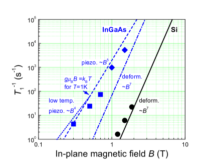
The Si crystal symmetry allows neither piezoelectricity nor a BIA SO term. SIA is dwarfed by an especially weak bulk SO coupling for valleys (estimated to be only – eV nm in comparable structures SIA in Si ). It was suggested in Nestoklon that linear-in- SO terms in (001) Si heterostructures are dominated by contributions of a low-symmetry heterointerface. For our typical electric fields, we estimate, with the help of Fig. 3 in Nestoklon , that has a maximum value of – eV nm for a perfect interface, but a much lower value in the presence of interface imperfections. In Fig. 5, in Si (with ) is shown by solid lines for (the numerically simulated) meV.
Other spin-lattice relaxation mechanisms were proposed for Si dots, in particular: (i) the modulation of the hyperfine coupling by phonon deformation, which has a field dependence Khaetskii ; Khaetskii2 , and (ii) the phonon-induced modulation of the bulk electron -factor, with a -dependence and a strong sensitivity to the orientation of the in-plane magnetic field with respect to the main crystallographic axes Glavin . As formulated, these mechanisms are not directly related to the heterointerface properties. They should exceed at extremely small magnetic fields, but the estimated times are too slow to be observed in our experiments.
Acknowledgements We gratefully acknowledge helpful discussions with M.A. Eriksson, H.W. Jiang, and C.M. Marcus. This work was sponsored by the United States Department of Defense. The views and conclusions contained in this document are those of the authors and should not be interpreted as representing the official policies, either expressly or implied, of the United States Department of Defense or the U.S. Government.
References
- (1) M. A. Eriksson et al., Quantum Information Processing 3, 133 (2004).
- (2) H.-W. Liu et al., Appl. Phys. Lett. 92, 222104 (2008); H.-W. Liu et al., Phys. Rev. B. 77, 073310 (2008); W. H. Lim et al., Appl. Phys. Lett. 94, 173502 (2009); A. Fuhrer et al., Nano Lett. 9, 707 (2009); L. H. Willems van Beveren et al., Appl. Phys. Lett. 93, 072102 (2008); G. P. Lansbergen et al., Nature Physics 4, 656 (2008). H. Sellier et al., Appl. Phys. Lett. 90, 073502 (2007).
- (3) C. B. Simmons et al., Appl. Phys. Lett. 91, 213103 (2007); M. R. Sakr et al., Appl. Phys. Lett. 87, 223104 (2005).
- (4) E. Croke, to be published .
- (5) J. M. Elzerman et al., Appl. Phys. Lett. 84, 4617 (2004).
- (6) J. M. Elzerman et al., Nature 430, 431 (2004).
- (7) U. Meirav and E. B. Foxman, Semicond. Sci. Tech. 11, 255 (1995).
- (8) D. K. Wilson and G. Feher, Phys. Rev. 124, 1068 (1961).
- (9) S. M. Reimann, Rev. Mod. Phys. 74, 1283 (2002).
- (10) Y. Hada and M. Eto, Phys. Rev. B 68, 155322 (2003).
- (11) To be published.
- (12) A. V. Khaetskii and Y. V. Nazarov, Phys. Rev. B 64, 125316 (2001).
- (13) L. M. Woods et al., Phys. Rev. B 66, 161318 (2002).
- (14) P. Stano and J. Fabian, Phys. Rev. Lett. 96, 186602 (2006); Phys. Rev. B 74, 045320 (2006).
- (15) Derived using InGaAs- and Si-specific data in Intrinsic Properties of Group IV Elements and III-V, II-VI, and I-VII Compounds, edited by O. Madelung, Landolt-Bo¨rnstein, New Series, Group III, Vol. 22, Pt. A (Springer, Berlin, 1987) and Semiconductors — Basic Data, edited by O. Madelung (Springer, Berlin, 1996); an isotropic elastic continuum is assumed; is calculated for our biased InGaAs structure and agrees well with the experiment.
- (16) Z. Wilamowski at al., Phys. Rev. B 66, 195315 (2002); C. Tahan and R. Joynt, Phys. Rev. B 71, 075315 (2005).
- (17) M. O. Nestoklon et al., Phys. Rev. B 77, 155328 (2008).
- (18) A. V. Khaetskii, Photonics Spectra 10, 27 (2001).
- (19) B. A. Glavin and K. W. Kim, Phys. Rev. B 68, 045308 (2003).