Highly efficient interfacing of guided plasmons and photons in nanowires
Abstract
Successful exploitations of strongly confined surface plasmon-polaritons critically rely on their efficient and rapid conversion to lossless channels. We demonstrate a simple, robust, and broad-band butt-coupling technique for connecting a metallic nanowire and a dielectric nanofiber. Conversion efficiencies above 95% in the visible and close to 100% in the near infrared can be achieved with realistic parameters. Moreover, by combining butt-coupling with nanofocusing, we propose a broad-band high-throughput near-field optical microscope.
Confined surface plasmon-polaritons (SPPs) have enormous potential for manipulating electromagnetic fields at optical frequencies and nanoscopic length scalesBarnes et al. (2003), with applications for interconnectsConway et al. (2007), field-enhanced spectroscopy and microscopyKeilmann (1999); Babadjanyan et al. (2000); Stockman (2004); Yeo et al. (2009), sensingSharma et al. (2007), and quantum opticsChang et al. (2006, 2007). However, absorption of energy at optical frequencies by real metals makes propagation of confined SPPs very lossy in comparison with the transmission of photons in dielectric guidesConway et al. (2007); Novotny and Hafner (1994). Therefore, practical device proposals require a rapid and efficient conversion of SPPs into photons. In case of SPPs at planar interfaces, evanescent wave and grating couplers are very effectiveRaether (1988). Thus, researchers have extended these schemes to guided modes of dielectric fibers (DF) and metallic wires (MW) in a side by side arrangementChang et al. (2006); Lee et al. (2008), via tapersKeilmann (1999); Bouhelier et al. (2003); Janunts et al. (2005); Ding et al. (2007), or by etching a grating on a MW nanoconeRopers et al. (2007). However, efficient implementation of these approaches requires an interaction length greater than a wavelengthSnyder and Love (1983), making losses an important issue. Furthermore, the critical dependence of evanescent coupling on the overlaps between the DF and MW modes, and the inherent wavelength dependence of grating coupling limit their bandwidths. In this Letter, we investigate the most straightforward and practical way of interfacing guided SPPs and photons between a MW and a nano DFTong et al. (2003) in an axially-symmetric butt-coupling scheme. We investigate the conversion process of photons to SPPs as a function of wavelength and material, identifying the moulding of SPPs at the coupling interface as the condition for reaching efficiencies above 95% in the visible and close to 100% in the near-infrared range. Furthermore, we present a practically feasible scheme to overcome the long-standing conflict between strong field enhancement and high throughput in scanning near-field optical microscopyNovotny et al. (1995), and to couple a quantum emitter to a propagating optical modeDomokos et al. (2002).

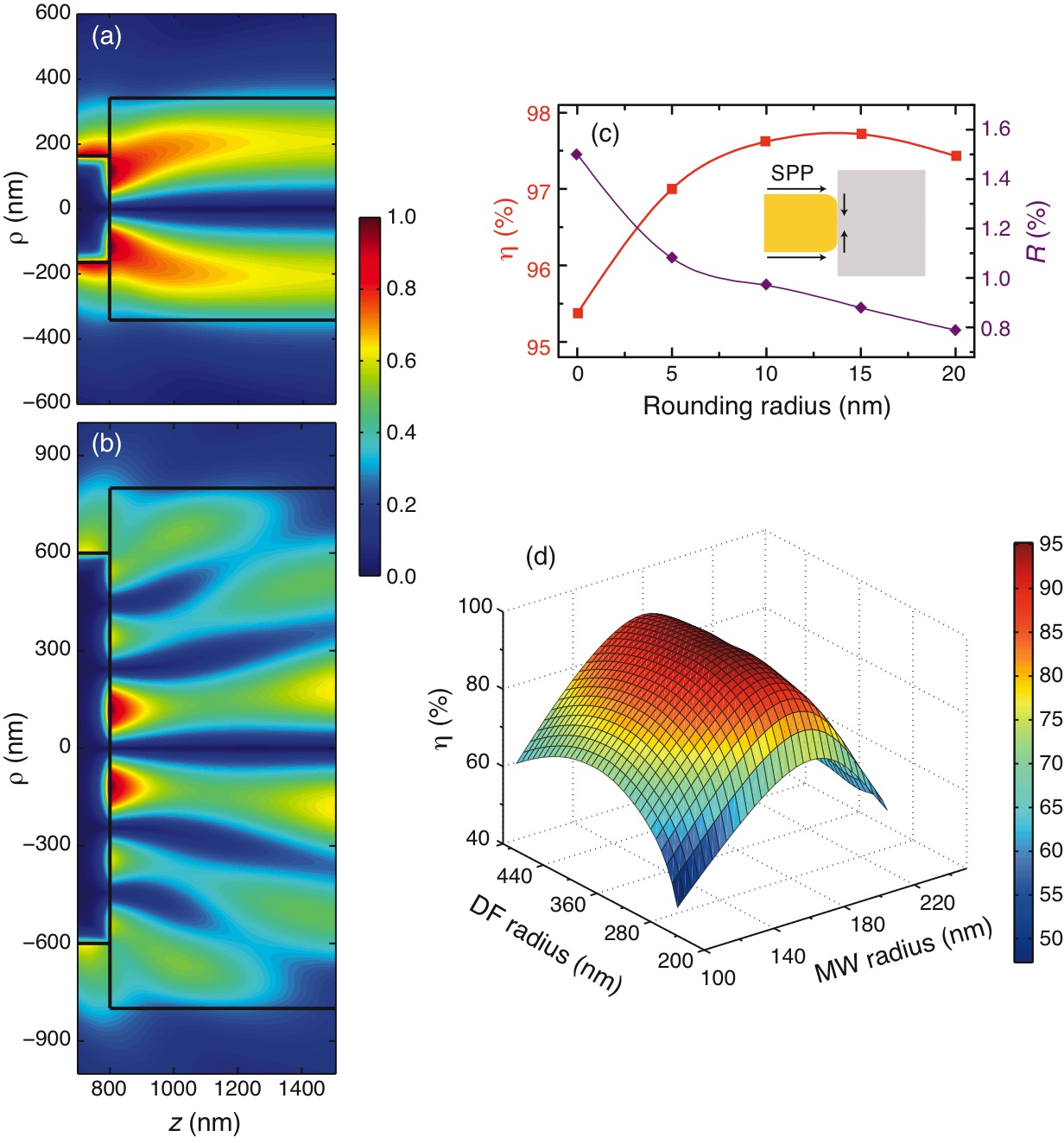
We performed body-of-revolution finite-difference time-domain (FDTD) calculationsTaflove and Hagness (2005) to trace the propagation of the optical signal along the guides in a rigorous and computationally efficient manner, and to acquire an intuitive understanding of the mode conversion. 1(a) and (f) sketch the geometrical arrangements for interfacing SPPs on a silverLide (2006) MW to guided photons in a silica DF and vice versa for a vacuum surrounding. The FDTD computational domain is restricted to the area enclosed by the dashed lines in 1(a) and (f), and its radial dimension is never less than two wavelengths. In each case, a steady-state SPP or a TM01 mode is launched from the left-hand side using the total-field/scatter-field techniqueTaflove and Hagness (2005). The dashed red lines in 1(a) and (f) mark the source, which separates the scattered-field from the total-field region. The Drude model with conductivity is used to account for the dispersive properties of metals. The parameters are deduced by fitting the tabulated experimental dataLide (2006); Palik and Ghosh (1998) across a small spectral range (100 nm). 1(k) and (l) depict the time-averaged transverse magnetic field profiles of the radially-polarized modes at the vacuum wavelength of nm in the DF and MW with radii of 342 nm and 164 nm, respectively. The snapshots of the magnetic field in 1(b)-(e) illustrate how SPPs travel on the surface of the MW and are converted to photons in the TM01 mode of the DF . To determine the conversion efficiency , we computed the ratio between the transmitted power in the guided mode right after the MW-DF interface and the incident power at the position right before it. The latter was calculated separately for an infinitely long MW or DF using the same source. In the example of 1(a), the MW and DF yielded =95%. We used a 2 nm grid here and found that the relative error between 1 nm and 2 nm grids is within 0.5%. A grid size of 0.5 nm is used for 2(c) and 5. 1(g)-(j) show the reverse situation where light originates in the silica DF and is converted to SPPs of the silver MW with the same efficiency as in the previous case. The great advantage of the butt-coupling scheme is that the conversion between SPPs and guided photons takes place across an interface. This feature minimizes the impact of propagation losses, which significantly increase as wavelength and MW radius decreaseNovotny and Hafner (1994). For instance, the MW at the wavelength considered in 1 would yeald losses as high as 0.72 dB/m.
To explore the underlying coupling mechanism, in 2(a) we plot the time-averaged magnetic field for the region between the dashed lines in 1(b). We find that the SPP moulds around the end of the MW (see arrows in the inset of 2(c)) in such a way that the magnetic field assumes a maximum value at a certain distance from the axis on the MW-DF interface. Here, we tuned the radii of the two guides to obtain an SPP field profile that optimizes its coupling to the TM01 mode of the DF. 2(b) displays another example of the field distribution for larger MW and DF radii of 600 nm and 800 nm, respectively. In this case the SPP magnetic field has three maxima, which clearly shows that the SPPs interfere and form a standing wave at the interface. Thus, a simple analysis based on mode-matching of the two guidesSnyder and Love (1983) of 1(a) only predicts =87% because it fails to account for the behaviour of SPPs. In fact, 2(c) shows that rounding off the MW edges facilitates this SPP folding process, improving and reducing reflections. Having demonstrated the possibility of very high conversion efficiency between SPPs and photons, it is important to examine the feasibility and reliability of this scheme for laboratory and technological applications. An important issue of concern is the fabrication tolerance. 2(d) displays as a function of the MW and DF radii at nm, revealing that conversion efficiencies greater than 90% can be achieved even if variations of up to 15% take place for the radii. Moreover, we have verified that even a structure with an air gap of up to 50 nm between the MW and DF would yield a conversion efficiency greater than 94%.
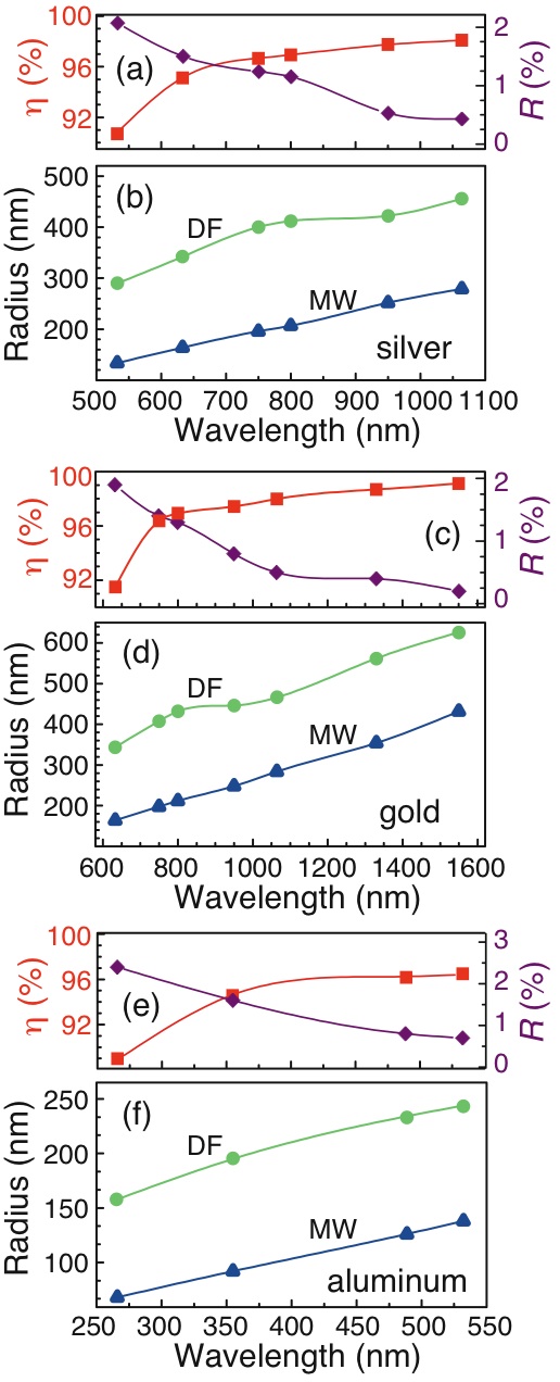
Next, we investigated the application of silver, goldLide (2006) or aluminiumPalik and Ghosh (1998) MW for operation at various wavelengths of interest in the visible, near infrared, and ultraviolet spectral regimes. We first found the radii by maximizing for a given wavelength using a mode-matching approachSnyder and Love (1983) and then applied the FDTD technique to optimize them in a rigorous manner, by scanning the radii around the previously estimated values. 3(a) shows that for the case of silver MW, increases from 91% to 98%, while reflection decreases from 2.1% to 0.4% as the wavelength grows over a spectral range greater than 500 nm. 3(b) plots the values of the silver-MW and silica-DF radii corresponding to each optimized case. The results for the opposite propagation direction are very similar (not shown). 3(c) and (d) show that if silver is replaced by gold, , and the corresponding radii yield similar values and trends. We note that around the telecommunication wavelength of 1550 nm, a gold MW transmits nearly 100% of the power to the DF. 3(e) and (f) display the same analysis for an aluminium MW with emphasis on the ultraviolet region, where a rapid conversion of SPPs and photons becomes more critical due to the very short SPP propagation length. We find that even at a wavelength as short as nm, can reach 89% if the DF and MW radii are respectively chosen to be 158 nm and 68 nm, for which the SPP propagation loss in the MW amounts to 3.62 dB/.
Variation of the DF material can be used to engineer the coupling device to match the confined SPP modes on thin MWs. As inferred from 2(a) and (b) the optimal radius of the MW can be reduced by a high-refractive-index DF also because the SPP standing wave on the coupling interface gets compressed by the larger wavenumber. 4(a) and (b) show the mode conversion properties for a gold MW at =1550 nm as a function of the refractive index of the DF. The optimal radii of the MW and DF decrease and converge to nearly the same value for larger DF refractive indices, while in each case can be optimized beyond 99%. As a last important property of concern, we examined the bandwidth of for a set of fixed MW and DF radii. 4(c) displays for a silver MW coupled to a silica DF in the visible range, and 4(d) shows the same for a gold MW coupled to a silicon DF in the near-infrared regime. These results demonstrate that bandwidths greater than 150 nm are fully within reach for over 90% conversion of SPPs to photons and vice versa.

We now discuss an immediate consequence of efficient and broad-band SPP-photon conversion between a MW and a DF from both directions. Over the last decade, several reports have pointed out that SPPs can be focused tightly to nanoscopic regions at metallic tipsKeilmann (1999); Babadjanyan et al. (2000); Stockman (2004). This phenomenon can indeed revolutionize high-resolution scanning near-field optical microscopy (SNOM), which has suffered from a very low transmission through small aperturesNovotny et al. (1995). However, so far there has been no viable approach for feeding optical energy into the SPP mode of the MW with a high efficiency. The device concept sketched in 5(a) provides an ideal solution for simultaneous intense and localized illumination as well as efficient collection. Furthermore, it is fully compatible with both state-of-the-art nanofabricationDe Angelis et al. (2008) and scanning implementation of fluorescence, Raman, or other nonlinear nanoscopiesSánchez et al. (1999); Ichimura et al. (2004).
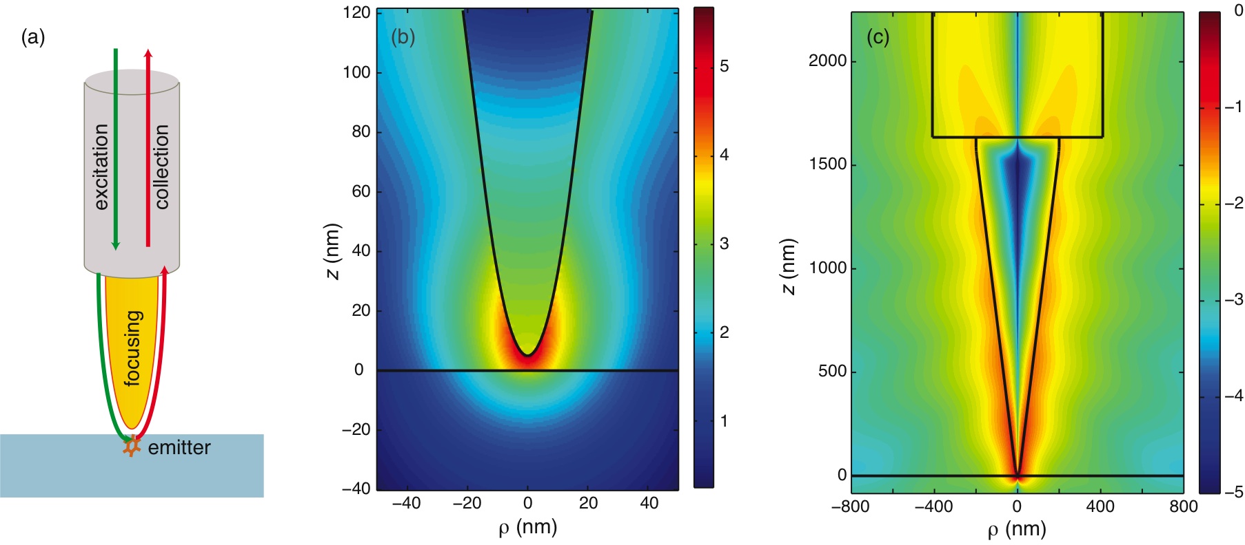
As a concrete example, we considered illumination at =730 nm and fluorescence collection at 780 nm from an emitter with a transition dipole moment oriented along the tip axis and embedded 5 nm below surface of a sample with a refractive index of 1.7. The excitation light was launched from a DF of 410 nm radius, coupled to a gold nanocone with an initial radius of 200 nm, and an opening angle of 14 degrees, which was terminated by a paraboloid. The tip was kept at a separation of 5 nm from the substrate. In 5(b) we plot the electric field intensity normalized to that of the source in the DF on a logarithmic scale for a zoom of a small region around the tip. The intensity is enhanced by more than 5 orders of magnitude and exhibits strong localization. 5(c) illustrates the emission process. We find that the radiated power is funnelled in the SPP and is then converted into the TM01 mode of the DF with an overall collection efficiency of about 70%, which is only limited by propagation loss and radiation along the nanocone.
We have shown that confined SPPs of a MW can be converted into guided photons of a dielectric nanofiber with a very high efficiency and large bandwidth using a simple butt-coupling scheme. For a given wavelength between the visible and the near infrared spectral range, one can always obtain larger than 95% by an appropriate choice of radius and material of the MW and DF. We have found that moulding of SPPs at the MW-DF interface plays a fundamental role in achieving these performances. Furthermore, we have discussed an important application of butt-coupling in the context of SNOM and nanofocusing, proposing a scanning probe that combines broad-band and high-throughput with high-spatial resolution. Efficient, broad-band and low-loss conversion of confined SPPs to guided photons is also key for a range of other applications such as high-resolution colour imagingKawata et al. (2008), on-chip manipulation and processing of quantum optical signalsDomokos et al. (2002); Chang et al. (2006, 2007) for implementation of quantum networksCirac et al. (1997), and actuation or sensing of physical, chemical, or biological processes at the molecular level,Zheng et al. (2009) paving the way for molecular-scale plasmonics.
We thank F. De Angelis and E. Di Fabrizio for fruitful discussions. This work was supported by ETH Zurich grant TH-49/06-1.
References
- Barnes et al. (2003) Barnes, W. L.; Dereux, A.; Ebbesen, T. W. Nature 2003, 424, 824–830
- Conway et al. (2007) Conway, J.; Sahni, S.; Szkopek, T. Opt. Express 2007, 15, 4474–4484
- Keilmann (1999) Keilmann, F. J. Microscopy 1999, 194, 567–570
- Babadjanyan et al. (2000) Babadjanyan, A. J.; Margaryan, N. L.; Nerkararyan, K. V. J. Appl. Phys. 2000, 87, 3785–3788
- Stockman (2004) Stockman, M. I. Phys. Rev. Lett. 2004, 93, 137404
- Yeo et al. (2009) Yeo, B.-S.; Stadler, J.; Schmid, T.; Zenobi, R.; Zhang, W. Chem. Phys. Lett. 2009, 472, 1–13
- Sharma et al. (2007) Sharma, A.; Jha, R.; Gupta, B. IEEE Sens. J. 2007, 7, 1118–1129
- Chang et al. (2006) Chang, D. E.; Sørensen, A. S.; Hemmer, P. R.; Lukin, M. D. Phys. Rev. Lett. 2006, 97, 053002
- Chang et al. (2007) Chang, D. E.; Sørensen, A. S.; Demler, E. A.; Lukin, M. D. Nat. Phys. 2007, 3, 807–812
- Novotny and Hafner (1994) Novotny, L.; Hafner, C. Phys. Rev. E 1994, 50, 4094–4106
- Raether (1988) Raether, H. Surface Plasmons on Smooth and Rough Surfaces and on Gratings; Springer-Verlag, 1988
- Lee et al. (2008) Lee, H. W.; Schmidt, M. A.; Tyagi, H. K.; Sempere, L. P.; Russell, P. S. J. Appl. Phys. Lett. 2008, 93, 111102
- Bouhelier et al. (2003) Bouhelier, A.; Renger, J.; Beversluis, M. R.; Novotny, L. J. Microscopy 2003, 210, 220–224
- Janunts et al. (2005) Janunts, N.; Baghdasaryan, K.; Nerkararyan, K.; Hecht, B. Opt. Commun. 2005, 253, 118–124
- Ding et al. (2007) Ding, W.; Andrews, S. R.; Maier, S. A. Phys. Rev. A 2007, 75, 063822
- Ropers et al. (2007) Ropers, C.; Neacsu, C. C.; Elsaesser, T.; Albrecht, M.; Raschke, M. B.; Lienau, C. Nano Lett. 2007, 7, 2784–2788
- Snyder and Love (1983) Snyder, A.; Love, J. Optical Waveguide Theory; Springer, 1983
- Tong et al. (2003) Tong, L.; Gattass, R. R.; B., A. J.; Sailing, H.; Jingyi, L.; Mengyan, S.; Iva, M.; Eric, M. Nature 2003, 426, 816–819
- Novotny et al. (1995) Novotny, L.; Pohl, D. W.; Hecht, B. Opt. Lett. 1995, 20, 970–972
- Domokos et al. (2002) Domokos, P.; Horak, P.; Ritsch, H. Phys. Rev. A 2002, 65, 033832
- Taflove and Hagness (2005) Taflove, A.; Hagness, S. Computational Electrodynamics: The Finite-Difference Time-Domain Method, 3rd ed.; Artech House: Norwood, MA, 2005
- Lide (2006) CRC Handbook of Chemistry and Physics, 87th ed.; Lide, D., Ed.; CRC Press, 2006
- Palik and Ghosh (1998) Handbook of Optical Constants of Solids; Palik, E. D., Ghosh, G., Eds.; Academic Press, 1998
- De Angelis et al. (2008) De Angelis, F.; Patrini, M.; Das, G.; Maksymov, I.; Galli, M.; Businaro, L.; Andreani, L. C.; Di Fabrizio, E. Nano Lett. 2008, 8, 2321–2327
- Sánchez et al. (1999) Sánchez, E. J.; Novotny, L.; Xie, X. S. Phys. Rev. Lett. 1999, 82, 4014–4017
- Ichimura et al. (2004) Ichimura, T.; Hayazawa, N.; Hashimoto, M.; Inouye, Y.; Kawata, S. Phys. Rev. Lett. 2004, 92, 220801
- Kawata et al. (2008) Kawata, S.; Ono, A.; Verma, P. Nat. Photon. 2008, 2, 438–442
- Cirac et al. (1997) Cirac, J. I.; Zoller, P.; Kimble, H. J.; Mabuchi, H. Phys. Rev. Lett. 1997, 78, 3221–3224
- Zheng et al. (2009) Zheng, Y. B.; Yang, Y.-W.; Jensen, L.; Fang, L.; Juluri, B. K.; Flood, A. H.; Weiss, P. S.; Stoddart, J. F.; Huang, T. J. Nano Lett. 2009, 9, 819–825