Tuning the electrical resistivity of semiconductor thin films by nanoscale corrugation
Abstract
The low-temperature electrical resistivity of corrugated semiconductor films is theoretically considered. Nanoscale corrugation enhances the electron-electron scattering contribution to the resistivity, resulting in a stepwise resistivity development with increasing corrugation amplitude. The enhanced electron scattering is attributed to the curvature-induced potential energy that affects the motion of electrons confined to a thin curved film. Geometric conditions and microscopic mechanism of the stepwise resistivity are discussed in detail.
1 Introduction
Nanostructures with curved geometry have attracted broad interest in the last decade. Successful fabrication of corrugated semiconductor films[1, 2], Möbius NbSe3 stripes[3], peanut-shaped C60 polymers[4, 5, 6], and other exotic nanomaterials with complex geometry[7, 8, 9, 10, 11, 12, 13, 14, 15] has triggered the development of next-generation nanodevices. Moreover, nanostructures provide an experimental platform for exploring the effects of surface curvature on the nature of conducting electrons confined to low-dimensional systems. An important consequence of non-zero surface curvature is the occurrence of a curvature-induced effective potential. It was theoretically suggested[16, 17, 18, 19] that an electron moving in a thin curved layer experiences potential energy whose sign and magnitude depend on the local geometric curvature. Such a curvature-induced potential has been observed to cause many intriguing phenomena[20, 21, 22, 23, 24, 25, 26, 27, 28, 29, 30, 31, 32, 33, 34, 35, 36, 37, 38, 39]: such as bound states of non-interacting electrons in deformed cylinders[40, 41, 42] and energy band gaps in periodic curved surfaces[43, 44, 45, 46]. Quite recently, surface curvature was found to markedly affect interacting electrons in the quasi-one dimension, resulting in a significant shift in the Tomonaga-Luttinger exponent of thin hollow cylinders subject to periodic surface deformation[47].
In the present study, we demonstrate an alternative consequence of surface curvature, which manifests in interacting electron systems. We consider the low-temperature resistivity of two-dimensional corrugated semiconductor films and show that nanoscale corrugation considerably enhances the resistivity of the films. This resistivity enhancement is attributed to contributions of electron-electron Umklapp scattering processes. When the amplitude of corrugation takes specific values determined by the Fermi energy, Umklapp processes due to the curvature-induced periodic potential cause a change in the total electron momentum, resulting in a significant increase in the resistivity. The period and amplitude of corrugations associated with the enhanced resistivity are within the realm of existing experiments[48], confirming the relevance of our theoretical predictions to curved-structure-based application technology.
This paper is organized as follows. In section 2, we provide an outline of the derivation of the Schödinger equation for a curved surface on the basis of the da Costa approach[17]. In section 3 and section 4, we summarize the formula for calculating the resistivity that is affected by electron-electron scattering on the periodically corrugated surface at low temperature. In section 5 and section 6, we present the numerical results and discussions, respectively. Finally, in section 7, we conclude the paper.
2 Electron eigenstates in nanocorrugated films
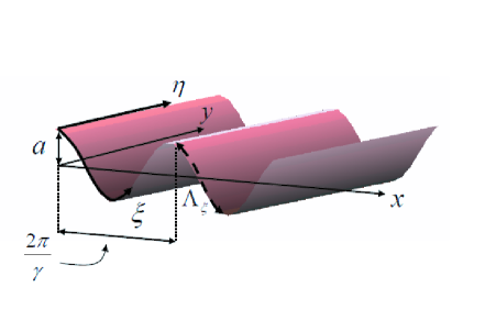
In this section, we outline the mathematical description of electrons confined to a periodically curved surface. We assume a thin conducting layer to which the motion of an electron is confined. The layer is corrugated in the -direction with period but remains flat in the -direction. The height of the layer is expressed as
| (1) |
where is the amplitude of corrugation (see Fig.1). We assume that the thickness of the layer is spatially uniform and sufficiently small to increase excitation energies in the normal direction far beyond those in the tangential direction. Under these conditions, we obtain the Schödinger equation for electrons propagating in the corrugated layer as[17]
where is the effective electron mass and . The salient feature of Eq.(2) is the presence of an attractive potential defined by
| (3) |
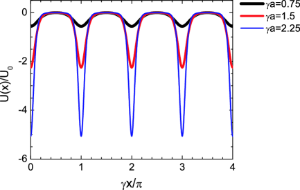
which results from the non-zero surface curvature of the system. (In fact, if , i.e. a flat surface.) Spatial profiles of in units of are shown in Fig.2, where several values of are selected. Downward peaks are formed at , where the layer height is either maximum () or minimum (). It is noteworthy that the -dependence of deviates considerably from a sinusoidal curve, whereas the surface corrugation is exactly sinusoidal.
Equation (2) is simplified by using new variables (see Fig.1):
| (4) |
Substituting them into Eq.(2) yields an alternative form of the Schrödinger equation
| (5) |
which has the solution of the form , with and satisfying the equations
| (6) | |||
| (7) |
where . From Eq.(7), we obtain . Equation (6) is solved by using the Fourier series expansions
| (8) |
and
| (9) |
where are integers; and represent the length of the layer along the - and -coordinate axes, respectively, and equals one period of (see Fig.1). Substituting Eqs.(8) and (9) into Eq.(6), we obtain the secular equation
| (10) |
where . Numerical diagonalization of Eq.(10) yields and that satisfy Eq.(6), which completes calculations of eigenstates of electrons confined to a thin corrugated layer.
3 Two-electron scattering processes: Umklapp and normal processes
The objective here is to determine the effect of electron-electron scattering processes on the low-temperature resistivity of thin corrugated layers. We assume a two-electron scattering process that transforms a pair of electron states () into (), where is the wave vector of the th degenerate eigenstate that belongs to a given Fermi energy . For the law of momentum conservation to hold, conditions
| (11) |
with arbitrary integer , and
| (12) |
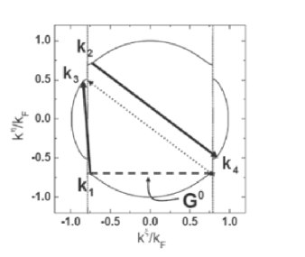
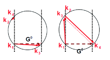
must be satisfied. The last term on the right side of Eq.(11) is attributed to the periodic structure of that yields a reciprocal lattice vector . A schematic illustration of a two-electron scattering process is shown in Fig.3. Thin curves on the - plane represent the Fermi surface for = 3.13 and = 1.32; these thin curves show gaps at , which are caused by the periodic potential . Here, we assume that in the absence of corrugation (i.e. ), the Fermi surface shows an exact circle on the - plane. As shown in Fig.3, two eigenstates located at and , in the vicinity of a corrugation-induced gap, are transformed into and , respectively. It should be noted that both relations (11) and (12) hold for the process shown in Fig.3, where the integer in Eq.(11) takes the value of . Hereafter, a two-electron scattering process involving an integer is termed the th Umklapp process; if , we refer to it as a normal scattering process.
4 Boltzmann transport equation
Contributions of two-electron scattering to the resistivity at low temperature are given by the Boltzmann transport equation[49]. We assume that and the Fermi surface has a circular shape on the - plane if . Then, we can prove that[50]
| (13) | |||||
| (14) |
where is the Boltzmann constant, is the group velocity of the electron belonging to the eigenstate , , and is the applied electric field. Integration over in Eq.(14) is carried out for all possible and that satisfy relations (11) and (12) for a fixed . The transition probability is given by
| (15) | |||||
where is the Fourier transform of the screened Coulomb potential[50] and in terms of the () coordinates. As is clear from Eq.(15), summations with respect to are carried out for all values under the constraints
| (16) |
where is fixed by the summation index in Eq.(14). In the actual calculation, we employed material constants of GaAs/AlxGa1-xAs heterostructures: meV, , and with a bare electron mass and the dielectrical constant of vaccum . In such heterostructures, the Fermi energy exists near the point, which justifies our assumption of an isotropic Fermi surface.
5 RESULTS
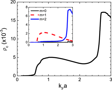
Figure 4 shows the -dependence of at nm-1. The surprising observation in Fig.4 is a stepwise increase in with , in which exhibits sudden jumps at specific values of given by = 0.6 and 2.6. The non-monotonic behaviour of plotted in Fig.4 suggests the possibility of tuning the resistivity of actual low-dimensional nanostructures by imposing surface corrugation. In fact, our results suggest that the corrugation-induced increase in the resistivity observed in -based nanocorrugated films with 5 nm and 40 nm is of the order of , which is within the range obtained by the measurement technique used in Refs.[48].
To determine the physical origin of jumps, we decompose the summation shown in Eq.(14) with respect to and separately plot three dominant components consisting of , as shown in the inset of Fig.4: the thin solid line shows the contribution of the normal scattering process (), the thin dotted line shows the contribution of the first-order Umklapp process (), and the thick solid line shows the contribution of the second-order Umklapp process (). The plot in the inset shows that the significant increase in the Umklapp contributions results in the jump in . The mechanism of the increase in Umklapp contributions is explained in detail in the next section.
We also find that specific values of which cause the jump in correspond to those of which satisfy the relation , or equivalently, , where is the Fermi wavelength. Figure 5 shows the -dependence of ; it decreases monotonically with , because and increases with (see Fig.5). We see from Fig.5 that takes the values of and at 0.6 and , respectively, which cause the jumps in as shown in Fig.4. It should be noted that at these values of , the radius of the Fermi circle on the - plane becomes equal to or . As a result, the gaps open at (as well as ), i.e. at both ends of the Fermi circle. These gaps lead to the increase in the Umklapp contribution to , as elucidated in the next section.
6 DISCUSSIONS
The jumps in shown in Fig.4 result from the following three conditions: i) enhanced transition probabilities in the integrand of , ii) divergence of the density of states (see Eq.(14)), and iii) occurrence of gaps at both the ends of the Fermi circle (i.e. at ). To present a concise argument, we consider first-order Umklapp contributions, i.e. components related to in expression (14). (An analogous discussion for the case of is available.)
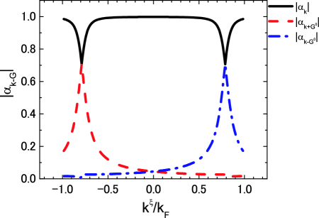
We know that includes the term , for instance. Here, has a large value within a limited region centred at (see Fig.6). It is noteworthy that larger results in larger ; furthermore, this scenario holds for other terms involving . Therefore, is enhanced when at least one of the four states, , is located with the corresponding region within which is large.
Next, we consider the condition for the density of states to diverge. From Ref.[50], it follows that
| (17) |
where and are the polar angles of and , respectively, on the - plane and is the relative angle between and . Expression (17) implies that diverges when and which correspond to forward and backward scattering, respectively, between the states of and . As a consequence, sudden jumps in are attributed to the Umklapp process that involves forward and backward scattering. Figure 7 shows some examples of relevant scattering processes that satisfy conditions i) and ii) mentioned earlier.
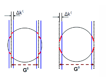
Finally, we comment on condition iii), that is, gaps in the Fermi surface should be positioned at both the ends of the Fermi circle, . Figure 8 shows two Fermi circles, in each of which gaps open at (a) and (b) . Circular thick arcs (coloured in red) indicate positions of eigenstates interior to the region of , i.e. states in the vicinity of gaps. From earlier discussions, it follows that Umklapp scattering processes involving the states indicated by thick curves significantly contribute to . It should be noted that such relevant processes are achieved more frequently in the Fermi circle shown in Fig.8(b) than in that shown in Fig.8(a), since the length of the thick curve in the former is larger than that in the latter. This proves that condition iii) is essential for the occurrence of the sudden jump in .
7 CONCLUSION
In conclusion, we have shown that the electrical resistivity of nanocorrugated semiconductor films exhibits a stepwise increase with the corrugation amplitude. Corrugation amplitudes that lead to resistivity jumps are determined by the relation , where is the Fermi wave vector and is the corrugation-induced reciprocal lattice vector associated with the curvature-driven periodic potential . We have proved that the resistivity jumps originate from the increased contribution of an Umklapp scattering process. The requisite corrugation amplitude and period for the resistivity jumps to be observable are within the realm of laboratory conditions, which confirms that our theoretical prediction can be verified experimentally.
Acknowledgments
We would like to thank K. Yakubo, S. Nishino, H. Suzuura, and S. Uryu for useful discussions and suggestions. This study was supported by a Grant-in-Aid for Scientific Research from the MEXT, Japan. One of the authers (H.S.) is thankful for the financial support from Executive Office of Research Strategy in Hokkaido University. A part of numerical simulations were carried out using the facilities of the Supercomputer Center, ISSP, University of Tokyo.
Appendix A The Schrödinger equation of corrugated nanofilms
This appendix describes the derivation of Eq.(2), i.e. the Schrödinger equation that describes the motion of electrons confined to a thin curved film. We assume that an electron located on a general curved surface is parameterised by , where is the position vector of an arbitrary point on the surface. According to the da Costa approach[17], the Schrödinger equation on the curved surface is given by
where is the effective mass of the electron, is the metric tensor defined by , is the inverse of , and [51]. The second term on the left side of Eq.(A) is the effective potential generated by the curvature of the system and is given by
| (19) |
where and are the so-called mean curvature and Gauss curvature of the surface, respectively. is the Weingarten curvature matrix expressed as
| (24) |
in which are the coefficients of the second fundamental form, , where is the unit vector normal to the surface,
| (25) |
Next, we consider a periodically corrugated surface parameterised by
| (26) |
where is a periodic function. From the definition of , we obtain
| (31) |
The unit normal is expressed as
| (32) |
which yields
| (37) |
Consequently, by substituting the above results into Eq.(19) and then assuming , we obtain the Schrödinger equation, i.e. Eq.(2). It should be emphasized that though our study focuses on unidirectionally corrugated films, our theoretical approach is applicable to a wide variety of nanostructures with periodically curved geometry, such as those suggested in Refs[52, 53].
References
References
- [1] Prinz V Ya, Grützmacher D, Beyer A, David C, Ketterer B and Deckardt E 2001 Nanotechnology 12 399
- [2] Prinz V Ya 2006 phys. stat. sol. (b) 243 3333
- [3] Tanda S, Tsuneta T, Okajima Y, Inagaki K, Yamaya K and Hatakenaka N 2002 Nature (London) 417 397
- [4] Onoe J, Nakayama T, Aono M and Hara T 2003 Appl. Phys. Lett. 82 595
- [5] Onoe J, Ito T, Kimura S, Ohno K, Noguchi Y and Ueda S 2007 Phys. Rev. B 75 233410
- [6] Onoe J, Ito T and Kimura S 2008 J. Appl. Phys. 104 103706
- [7] Lorke A, Bohm S and Wegscheider W 2003 Superlattices Microstruct. 33 347
- [8] McIlroy D N, Alkhateeb A, Zhang D, Aston D E, Marcy A C and Norton M G 2004 J. Phys.: Condens. Matter 16 R415
- [9] Sano M, Kamino A, Okamura J and Shinkai S 2004 Science 293 1299
- [10] Gao P X, Ding Y, Mai W J, Hughes W L, Lao C S and Wang Z L 2005 Science 309 1700
- [11] Yang S, Chen X, Motojima S and Ichihara M 2005 Carbon 43 827
- [12] Wang L, Major D, Paga P, Zhang D, Norton M G and McIlroy D N 2006 Nanotechnology 17 S298
- [13] Gong Z, Niu Z and Fang Z 2006 Nanotechnology 17 1140
- [14] Fujita T, Qian L H, Inoke K, Erlebacher J and Chen M W 2008 Appl. Phys. Lett. 92 251902
- [15] Sainiemi L, Grigoras K and Franssila S 2009 Nanotechnology 20 075306
- [16] Jensen H and Koppe H 1971 Ann. Phys. 63 586
- [17] da Costa R C T 1981 Phys. Rev. A 23 1982
- [18] Kaplan L, Maitra N T and Heller E J 1997 Phys. Rev. A 56 2592
- [19] Schuster P C and Jaffe R L 2003 Ann. Phys. 307 132
- [20] Mostafazadeh A 1996 Phys. Rev. A 54 1165
- [21] Entin M V and Magarill L I 2001 Phys. Rev. B 64 085330
- [22] Entin M V and Magarill L I 2002 Phys. Rev. B 66 205308
- [23] Encinosa M and Mott L 2003 Phys. Rev. A 68 014102
- [24] Bulaev D V, Geyler V A and Margulis V A 2004 Phys. Rev. B 69 195313
- [25] Chaplik A V and Blick R H 2004 New J. Phys. 6 33
- [26] Entin M V and Magarill L I 2004 Europhys. Lett. 68 853
- [27] Olendski O and Mikhailovska L 2005 Phys. Rev. B 72 235314
- [28] Gravesen J and Willatzen M 2005 Phys. Rev. A 72 032108
- [29] Encinosa M 2006 Phys. Rev. A 73 012102
- [30] Zhang E, Zhang S and Wang Q 2007 Phys. Rev. B 75 085308
- [31] Atanasova V and Dandoloff R 2007 Phys. Lett. A 371 118
- [32] Balakrishnan R and Dandoloff R 2008 Nonlinearity 21 1
- [33] Olendski O and Mikhailovska L 2008 Phys. Rev. B 77 174405
- [34] Atanasova V and Dandoloff R 2008 Phys. Lett. A 372 6141
- [35] Ferrari G and Cuoghi G 2008 Phys. Rev. Lett. 100 230403
- [36] Ferrari G, Bertoni A, Goldoni G and Molinari E 2008 Phys. Rev. B 78 115326
- [37] Atanasova V and Dandoloff R and Saxena A 2009 Phys. Rev. B 79 033404
- [38] Cuoghi G, Ferrari G and Bertoni A 2009 Phys. Rev. B 79 073410
- [39] Atanasova V and Dandoloff R 2009 Phys. Lett. A 373 716
- [40] Cantele G, Ninno D and Iadonisi G 2000 Phys. Rev. B 61 13730
- [41] Marchi A, Reggiani S, Rudan M and Bertoni A 2005 Phys. Rev. B 72 035403
- [42] Taira H and Shima H 2007 Surf. Sci. 601 5270
- [43] Aoki H, Koshino M, Takeda D and Morise H 2001 Phys. Rev. B 65 035102
- [44] Fujita N 2004 J. Phys. Soc. Jpn. 73 3115
- [45] Koshino M and Aoki H 2005 Phys. Rev. B 71 073405
- [46] Fujita N and Terasaki O 2005 Phys. Rev. B 72 085459
- [47] Shima H, Yoshioka H and Onoe J arXiv:0903.0798
- [48] Messica A, Soibel A, Meirav U, Stern A, Shtrikman H, Umansky V and Mahalu D 1997 Phys. Rev. Lett 78 705
- [49] Ziman J M 2001 Electrons and Phonons Oxford University Press, New York
- [50] Uryu S and Ando T 2001 Phys. Rev. B 64 195334
- [51] Shima H and Nakayama T 2009 Higher Mathematics for Physics and Engineering (Springer-Verlag)
- [52] Arias I and Arroyo M 2008 Phys. Rev. Lett. 100 230403
- [53] Shima H and Sato M 2008 Nanotechnology 19 495705