M.i.p. detection performances of a 100 read-out CMOS pixel sensor with digitised outputs
Abstract
Swift, high resolution CMOS pixel sensors are being developed for the ILC vertex detector, aiming to allow approaching the interaction point very closely. A major issue is the time resolution of the sensors needed to deal with the high occupancy generated by the beam related background. A 128x576 pixel sensor providing digitised outputs at a read-out time of 92.5 , was fabricated in 2008 within the EU project EUDET, and tested with charged particles at the CERN-SPS. Its prominent performances in terms of noise, detection efficiency versus fake hit rate, spatial resolution and radiation tolerance are overviewed. They validate the sensor architecture.
1 Introduction
The ambitionned impact parameter resolution at the ILC calls for a highly granular and transparent pixellised vertex detector with an inner radius well below 2 centimetres. Approaching the interaction point so closely exposes the pixel sensors equipping the detector to high rates of beam-related background, dominated by beamstrahlung electrons. The latter govern the time resolution and the radiation tolerance required for the sensors.
CMOS pixel sensors are attractive for this application because of their high granularity and thin sensitive volume. Adapting them to the ILC vertex detector drives an R&D effort mainly oriented towards a high read-out speed, while ensuring that the sensors tolerate the radiation level foreseen.
IPHC-Strasbourg and IRFU-Saclay are developing such sensors within the European FP6 project EUDET [2], to equip a pixellised beam telescope providing a few micrometer resolution over each of its six, 1x2 cm2 large, planes read out at a frequency of 104 frames per second. Details on the sensor design are provided in [3].
To accommodate the data rate, the signals delivered by the sensors are discriminated before being filtered by an integrated zero-suppression logic. A fast read-out is achieved by grouping the pixels composing the sensitive area in columns read out in parallel. The development of this architecture relies on two parallel tasks. One of them addresses the upstream part of the signal collection and conditionning chain, including the pixel array and the discriminators ending the columns. The other concerns the downstream part, combining a zero-suppression logic with output memories.
2 Pixel array with binary outputs
Small prototypes were fabricated and tested in previous years to develop the upstream part of the sensor architecture [4]. MIMOSA-22 is the last prototype of this R&D line before realising the final sensor for the EUDET telescope. Two complementary versions were designed and fabricated [3]. They feature 136 columns read out in parallel, each made of 576, 18.4 pitch, pixels. 128 columns are ended with a discriminator, while 8 columns have analogue outputs for test purposes. The chip incorporates a JTAG controller. The frame read-out time is 92.5 . Various pixel designs were integrated in the chip, allowing to explore different sensing diode sizes, amplification schemes, ionising radiation tolerant designs, etc.
The sensors were characterised in 2008, first in the laboratory with an 55Fe source and next at the CERN-SPS, mounted on a silicon-strip beam telescope. A modest noise value was found for most pixel designs, ranging from about 10 to 14 e-ENC at room temperature, with a mild operating temperature dependence. The 128 discriminators exhibited a modest threshold dispersion ( 4 % standard deviation) and contributed marginally to the total noise. No significant non-uniformity was found over the sensitive area of any of the 6 sensors tested.
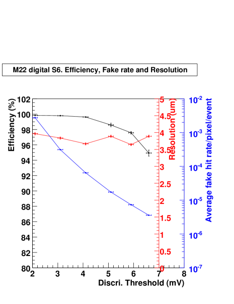
When exposed to a 120 GeV beam at the CERN-SPS, a signal-to-noise ratio in the range 17–21 (most probable value) was measured, depending on the pixel design. Figure 1 displays the measured detection performances of one sub-array (detection efficiency, single point resolution, average fake hit rate ) as a function of the discriminator thresholds.
The observed detection efficiency remains 99.5 % for threshold values high enough to keep the fake hit rate 10-4, avoiding the signal processing micro-circuits to be saturated by pixel noise fluctuations. The single point resolution is 4 , well suited to the detector outer layers and close to the value required for the inner layers ( 3 ). Reducing the pitch by 20% will suffice to reach this goal.
These appealing results were complemented with a first study of the sensor tolerance to ionising radiation. The expected annual dose at the ILC is O(1) kGy in the innermost layer, due to beamstrahlung electrons. The detection performances of a sensor exposed to 1.5 kGy (10 keV X-Ray source ) were assessed at the CERN-SPS with the 120 GeV beam mentionned earlier. Despite a 30 % noise increase, the detection efficiency was still above 99.5 % for a fake rate 10-4. The noise increase is due to the amplification circuitry integrated in the pixels. Its design is being improved, aiming for 10 kGy tolerance.
Summarising, the MIMOSA-22 architecture is validated for its integration in the final EUDET sensor.
3 Zero-suppression micro-circuit
SUZE-01 incorporates the zero-suppression micro-circuit and output memories composing the downstream part of the sensor architecture. Its logic is intended to be integrated right after the discriminators of MIMOSA-22 in the final sensor.
The circuitry is organised in a 3 stage pipeline, adapted to the output of 128 columns [3]. In the first stage, the input signals (discriminator outputs) are distributed over banks, each encompassing 64 columns, where a sparse data scan algorithm on hit pixels is performed. Up to 4 contiguous pixel signals (called ”string” hereafter) above threshold are encoded in a 2 bit state word. Up to 6 strings per bank can be memorised with column addresses. The address of a string shared by two neighbouring banks is transferred only once. The second stage combines the outcomes of the two banks of the first stage. Its multiplexing logic accepts up to 9 strings per pixel row and adds the bank address information. The results of the second stage are stored in the third stage, i.e. a 96 kbit memory split in 2 buffers, allowing a continuous read-out via a LVDS link at 160 MHz.
Fabricated in 2007, SUZE-01 was tested extensively at IPHC with millions of patterns at its nominal clock frequency (100 MHz) and above. No failures were spotted for frequencies 115 MHz. The architecture is thus validated for its integration in the final EUDET sensor.
The EUDET telescope specifications, are quite similar to those of the ILC vertex detector outer layers. For the inner layers, the maximal number of strings per stage, the memory capacity and the transfer frequency still need to be extended.
4 Full size pixel array with integrated zero suppression
The final EUDET sensor (called MIMOSA-26) was designed in 2008 and sent for fabrication. It combines the architecture of MIMOSA-22 and SUZE-01 in a comprehensive charge sensing and signal read-out chain, providing discriminated signals in a binary mode including the pixel address. It features 1152 columns of 576 pixels, read out in 100 . It will be commissionned in 2009, mounted on the EUDET telescope. If satisfactory, this architecture will next be adapted to the outer layers of the vertex detector, which require about 100 read-out time. It will also be evolved towards shorter read-out times, aiming for a target value of 25 for the innermost layer.
References
-
[1]
Presentation:
http://ilcagenda.linearcollider.org/contributionDisplay.py?contribId=213&sessionId=21&confId=2628 - [2] EUDET collaboration, Detector R&D towards the International Linear Collider, supported by the E.U. within FP6, http://www.eudet.org/.
- [3] C.Hu-Guo et al., CMOS sensor development: a fast read-out architecture with integrated zero suppression, contribution to the Pixel-08 Workshop, Chicago/USA (September 2008), to be pulished in Nucl. Inst. Meth. A.
- [4] A. Besson et al., MIMOSA-16 Final Tests, EUDET meeting, DESY/Hamburg (January 2008).