Pseudospin valve in bilayer graphene: towards graphene-based pseudospintronics
Abstract
We propose a non-magnetic, pseudospin-based version of a spin valve, in which the pseudospin polarization in neighboring regions of a graphene bilayer is controlled by external gates. Numerical calculations demonstrate a large on-off ratio of such a device. This finding holds promise for the realization of pseudospintronics: a form of electronics based upon the manipulation of pseudospin analogous to the control of physical spin in spintronics applications.
pacs:
75.70.Ak, 75.47.Pq, 85.75.-d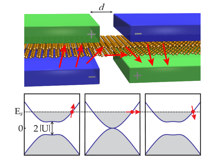
Soon after its discovery novo04 , it was realized that graphene supports an additional quantum number called pseudospin novo05 ; zhang05 ; geimrev that arises because the honeycomb lattice is composed of two triangular sublattices. Wave-function amplitudes can be written like the two components of a spin- elementary particle, and electrons in graphene display characteristics analogous to relativistic fermions novo05 ; zhang05 . In particular, this includes the celebrated effect of chirality, whose profound consequences include an unusual sequencing of plateaus in measurements of the quantum Hall effect novo05 ; zhang05 ; novo06 , suppression of backscattering ando98 ; mceuen99 and Klein tunneling at interfaces kats06 ; chei06 .
So far, it has not been possible to exploit the pseudospin degree of freedom in graphene in a similar way as physical spin in spintronics spintronics and quantum computing loss98 applications. In a monolayer of graphene, chirality means that the orientation of an electron’s pseudospin is inextricably linked to the direction of its momentum, thus constraining the pseudospin to lie in the plane of the graphene sheet and preventing its use as an independently-tunable degree of freedom. In bilayers of graphene novo06 ; mcc06 ; ohta06 , the pseudospin degree of freedom is associated with the electronic density on the two layers. The constraint of chirality entails that electronic density is equally divided between the two layers so that the pseudospin again lies in the plane of the layers but now turning twice as quickly as the direction of momentum novo06 ; mcc06 . Min et al min08 were the first to realize that bilayers still offer a promising platform for pseudospintronics. In particular, they predicted that a pseudomagnetic state can form spontaneously due to strong Coulomb interactions at vanishing charge-carrier density; this effect is intimately tied to the fact that the density of states remains finite because the dispersion relation is parabolic, in contrast to the situation in a monolayer.
In this Letter we propose a variant of graphene-based pseudospintronics which exploits another direct advantage of a bilayer over a monolayer, namely the facility to induce a difference between the on-site energies on the two layers via a perpendicularly applied electric field, which can be realized by pairs of gate electrodes (see Fig. 1). The resulting asymmetry of the layers induces an energy gap between the conduction and valence bands mcc06 ; guinea06 ; mcc06b ; min07 , as observed in photoemission ohta06 and transport oostinga ; castro measurements. For states above or below the gap, interlayer asymmetry has the effect of creating an “up” or “down” component of pseudospin perpendicular to the electronic momentum and the plane of the sheet mcc06 ; min08 . The electric field hence acts on the pseudospin in the same way as a magnetic field acts on the physical spin of electrons in spintronic applications. In particular, the preferred pseudospin direction can be switched by inverting the sign of the applied potential difference. In analogy to the giant magnetoresistance (GMR) induced by a domain wall boundary in magnetic materials gmr ; viret , one would therefore expect that interfaces between regions of different gate polarity inhibit the flow of electrons. We will demonstrate that this effect can indeed be utilized to realize an all-electronic, pseudospin-based analogue of a spin valve with a large on-off ratio.
Concepts.—The proposed pseudospin valve can be realized in a sheet of bilayer graphene with sets of gates which produce a spatial variation of interlayer asymmetry in the direction of current flow (see Fig. 1). Top and bottom gates are used to independently control the Fermi level and the interlayer asymmetry, the latter creating an out-of-plane component of pseudospin. When the polarity of the two pairs of gates is identical, the device is in its “parallel” configuration, and offers only a small resistance to the flow of electrons with energies above the gap. The illustration in Fig. 1 shows the device in its “anti-parallel” configuration, which is realized when the polarity of the gates changes sign across the device. This produces a corresponding rotation of the pseudospin polarization with a switching of the out-of-plane component. Similarly to spin scattering at domain walls viret , the pseudospin of an incoming electron will precess about the changing local polarization as it attempts to follow it. If the change in the polarization rotation is sharp enough, the re-alignment of the electron’s pseudospin should only be partially successful, leading to reflection and a drop in the flow of current through the device.
We characterize the fidelity of the pseudospin valve in terms of the pseudo-magnetoresistance () ratio
| (1) |
which is defined by the resistances (parallel configuration) and (antiparallel configuration) determining the current flowing through the device in response to an applied bias voltage difference . The resistance ratio is the analogue of the conservative definition of magnetoresistance in spintronic applications spintronics ; viret , and takes the value for a perfect spin valve.
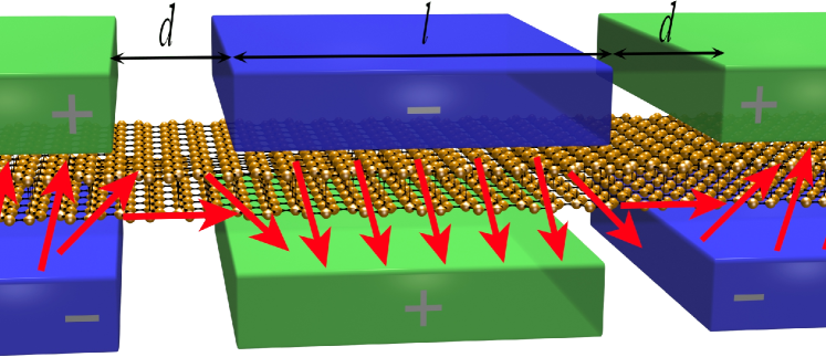
As in conventional spintronic applications, we also consider how the pseudospin-valve effect can be extended to a broader range of energies via serial connection of regions of different polarity. This leads to the design of a pseudospin-valve transistor operated by switching the polarity of a central gate of length (shown in Fig. 2).
Numerical results.—We start with numerical results, which are based on the microscopic tight-binding model of bilayer graphene. This model offers an accurate description of electronic transport in terms of a small number of characteristic energies and length scales. Transport between carbon atoms in a single layer (arranged on a honeycomb lattice with bond length Å) is described by kinetic hopping energy eV, which also determines the Fermi velocity of an isolated monolayer. In a bilayer, the two sheets of carbon are arranged according to Bernal stacking, whereby half of the atoms are strongly coupled to an atom in the other layer, with a strength determined by the interlayer coupling parameter eV. Additional next-nearest neighbor couplings are non-essential for the problem at hand, and are therefore neglected for simplicity.
In the parallel configuration, the spatially constant on-site potential takes the value in the top layer and in the bottom layer. In the anti-parallel configuration of the device we model the on-site potential by
| (2) |
where is the error function and is the coordinate in the direction of transport. The main design parameters of the pseudospin valve are the typical length scale of variation of the gate potential and the magnitude of the potential value at large distance, as well as the Fermi energy which determines the energy at which the electrons are injected from the electrodes ( for a charge-neutral gapless bilayer). In the parallel configuration, the presence of a homogeneous symmetry-breaking onsite potential opens an energy gap around the Fermi energy of the charge-neutral bilayer (see again Fig. 1). For the antiparallel configuration with the inhomogeneous potential of Eq. (2), the solution of the tight-binding model requires, in general, a numerical approach.
Since is independent, the problem of an infinitely wide ribbon is separable, and electronic modes with fixed transverse wavenumber decouple. For each transverse mode, the problem can be reduced to a one-dimensional chain of coupled bilayer unit cells, where each unit cell is composed of four carbon atoms. The Green function of each chain can be computed efficiently using the recursive Green function technique datta , which delivers the transmission amplitude via the Fisher-Lee formula fisherlee . In the linear response regime, the total phase-coherent conductance of the nanoribbon is then obtained from the Landauer formula. For a ribbon of finite width , the following considerations remain valid as long as and , so that the contribution of edges can be neglected (see the discussion at the end of the paper).
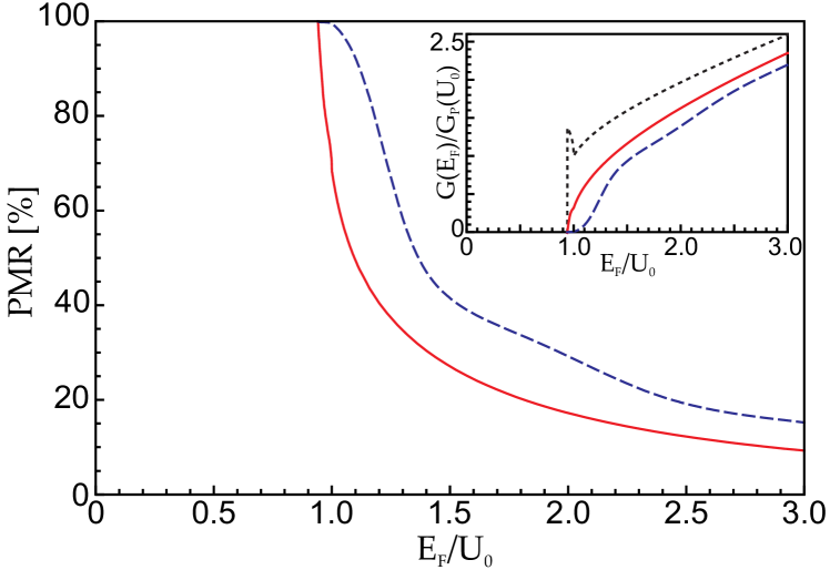
The calculated conductance versus Fermi energy is shown in the inset of Fig. 3 for the parallel configuration, as well as the antiparallel configuration with one or two interfaces. In these calculations, the interface parameters are and , respectively, and the asymptotic gap is eV, corresponding to parameters which can be realized in present bilayer experiments ohta06 ; castro . We find that close to the band edge the conductance in the antiparallel configuration is strongly reduced below its value in the parallel configuration. The resulting ratio is plotted in the main panel of Fig. 3. For energies just above the gap, the peaks at . For increasing Fermi energy the resistance ratio drops, which can be attributed to the decreasing out-of-plane component of the pseudospin of incoming electrons as they become less sensitive to the asymmetry of the layers when their kinetic energy increases. As expected from the GMR analogy, the presence of a second interface in the pseudospin-valve transistor (dashed line) significantly extends the energy range over which the is .
Analytical considerations.—A qualitative analysis of the pseudospin-valve effect can be achieved by considering the low-energy physics of gapped graphene bilayers. The microscopic tight-binding Hamiltonian delivers a band structure with four bands. For realistic values of the charge carrier density, the Fermi surface of bilayer graphene lies in the vicinity of two valleys, indexed by , situated at the K and K’ point at the corners of the hexagonal Brillouin zone. Owing to the interlayer coupling, two of the bands are split away by an energy . For the interlayer asymmetries and Fermi energies assumed in this work, these split bands do not contribute to the electronic transport. In the absence of layer asymmetry, the two remaining bands touch at zero energy and have an approximately parabolic dispersion relation , with effective mass and corresponding Fermi velocity .
To explain the influence of interlayer asymmetry, we employ a two-component Hamiltonian mcc06 that approximately describes the electronic behavior in these two low-energy bands,
The effective Hamiltonian operates in a space of two-component wave functions describing electronic amplitudes on the top and bottom layers. The first term in the Hamiltonian corresponds to a pseudospin-orbit coupling and ensures chirality of the electronic states in the absence of a symmetry-breaking on-site potential. The second term in takes into account the influence of external gates that produce different on-site energies on the two layers. This term is analogous to the Zeeman energy of a physical spin in a magnetic field parallel to the direction and leads to a gap in the electronic spectrum . The pseudospin part of the corresponding wave functions takes the form
where is the angle of the momentum in the plane . The pseudospin of such a state is
For energy near the vicinity of the gap , the out-of-plane component takes its maximum value , whereas it is reduced away from the gapped region.
The pseudospin-valve effect proposed in the present paper originates in the large resistance at interfaces between regions of opposite preferred pseudospin direction. This resistance arises because the pseudospin degree of freedom can adjust itself to such a spatial variation only over a distance , as follows from the scaling of the different terms in the two-component model. This pseudospin precession length scale is comparable to the Fermi wavelength, which is the scale on which chirality is established in the symmetric bilayer.
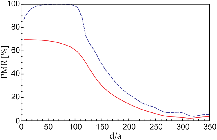
In both devices studied, the amount of reflection of incoming electrons in the anti-parallel configuration will therefore depend on the sharpness of the interface as compared to the pseudospin precession length . Figure 4 shows the computed dependence of the resistance ratio on for fixed values of eV. For these parameters, the pseudospin precession length . In the regime of an abrupt interface, the electron’s pseudospin is not able to rotate quickly enough to accommodate the change, which causes reflection and a large spin-valve effect. The series connection of two interfaces in the transistor further increases the resistance ratio to almost , except for very small values of where the resistance in the antiparallel arrangement drops due to tunneling through the central region. In the opposite limit , the pseudospin of incoming electrons is able to adiabatically adapt itself to the change of local polarization. In this limit the pseudospin-valve effect becomes negligible both for the single interface as well as for the series connection of two interfaces. The numerical results confirm that the transition between both regimes occurs at . The pseudospin-valve effect can therefore be realized in devices with gate separation of the order of a few tens of nanometers.
Discussion and Conclusions.—The large mobility of charge carriers in graphene has stimulated intense research efforts that aim at the realization of graphene-based electronic devices. In particular, manipulation of the differential population of valley states in momentum space has been proposed ryc07 , leading to a “valleytronic” analogy of spintronics. Our proposal of bilayer-based pseudospintronics relies on differential population of atomic orbitals in real space. This offers a robust mechanism to exploit spintronic analogies without the necessity of carefully fabricated nanoribbon edges, which limit the scalability of valleytronics falko and induce harmful intervalley scattering akh08 .
In particular, pseudospintronics relies on bulk effects which do not depend on the crystallographic orientation of the interface. For the wide samples considered here (), effects from the sample edges can be neglected since (i) edge states are localized at realistic rough edges, (ii) hypothetical clean edges at most contribute an additional transport channel per spin, and (iii) intervalley scattering off the edges can contribute to pseudospin relaxation across the interface, but this effect is negligible for . Pseudospintronics is also remarkably robust against bulk disorder. Chirality guarantees that the bulk pseudospin-flip rate for majority carriers in a clean ballistic bilayer is zero (the out-of plane polarization of the pseudospin in the leads is valley-independent). The predominant scattering mechanism in graphene, Coulomb scattering off charged impurities, does not break chirality moro08 ; adam08 . Inter-valley scattering contributes to pseudospin-flip scattering in the interface region, but the scattering lengths reported in recent experiments Gorbachev indicates that this does not add an additional constraint on .
Additional advantages of the proposed bilayer pseudospintronics concept arise from the fact that the charge carrier densities are finite. In devices that involve positioning the Fermi level within the bandgap, including field-effect transistors oostinga or valley filters based on topologically-confined channels between insulating regions martin , the effective gap size is reduced by screening mcc06b ; min07 . Under these conditions, the largest gaps observed so far in experiment are of the order of meV K oostinga . A finite charge density admits far larger gaps with experimental values reaching meV K ohta06 ; castro at high density.
We thank V. I. Fal’ko and C. Poole for helpful discussions. This research was supported by the European Commission, Marie Curie Excellence Grant MEXT-CT-2005-023778, and by EPSRC First Grant EP/E063519/1.
References
- (1) K. S. Novoselov et al., Science 306, 666 (2004).
- (2) K. S. Novoselov et al., Nature 438, 197 (2005).
- (3) Y. B. Zhang, Y. W. Tan, H. L. Stormer and P. Kim, Nature 438, 201 (2005).
- (4) A. K. Geim and K. S. Novoselov, Nature Mater. 6, 183 (2007).
- (5) K. S. Novoselov et al., Nature Phys. 2, 177 (2006).
- (6) T. Ando, T. Nakanishi, and R. Saito, J. Phys. Soc. Jpn. 67, 2857 (1998).
- (7) P. L. McEuen et al., Phys. Rev. Lett. 83, 5098 (1999).
- (8) M. I. Katsnelson, K. S. Novoselov, and A. K. Geim, Nature Phys. 2, 620 (2006).
- (9) V. V. Cheianov and V. I. Fal’ko, Phys. Rev. B 74, 041403(R) (2006).
- (10) M. A. M. Gijs and G. E. W. Bauer, Advances in Physics 46, 285 (1997).
- (11) D. Loss and D. P. DiVincenzo, Phys. Rev. A 57, 120 (1998).
- (12) E. McCann and V. I. Fal’ko, Phys. Rev. Lett. 96, 086805 (2006).
- (13) T. Ohta et al., Science 313, 951 (2006).
- (14) H. Min, G. Borghi, M. Polini and A. H. MacDonald, Phys. Rev. B 77, 041407(R) (2008).
- (15) F. Guinea, A. H. Castro Neto, and N. M. R. Peres, Phys. Rev. B 73, 245426 (2006).
- (16) E. McCann, Phys. Rev. B 74, 161403(R) (2006).
- (17) H. Min, B. Sahu, S. K. Banerjee and A. H. MacDonald, Phys. Rev. B 75, 155115 (2007).
- (18) J. B Oostinga, H. Heersche, X. Liu and A. Morpurgo, Nature Mater. 7, 151 (2007).
- (19) E. V. Castro et al., Phys. Rev. Lett. 99, 216802 (2007).
- (20) M. N. Baibich et al., Phys. Rev. B39, 4828 (1989).
- (21) M. Viret et al., Phys Rev. B 53, 8464 (1996).
- (22) S. Datta, Electronic Transport in Mesoscopic Systems (Cambridge University Press, Cambridge, 1997).
- (23) D. S. Fisher, P. A. Lee, Phys. Rev. B 23, 6851 (1981).
- (24) A. Rycerz, J. Tworzydlo, and C. W. J. Beenakker, Nature Phys. 3, 172 (2007).
- (25) V. I. Fal’ko, Nature Phys. 3, 151 (2007).
- (26) A. R. Akhmerov, J. H. Bardarson, A. Rycerz, and C. W. J. Beenakker, Phys. Rev. B 77, 205416 (2008).
- (27) S. V. Morozov et al., Phys. Rev. Lett. 100, 016602 (2008).
- (28) S. Adam and S. Das Sarma, Phys. Rev. B 77, 115436 (2008).
- (29) R. V. Gorbachev et al., Phys. Rev. Lett. 98, 176805 (2007).
- (30) I. Martin, Ya. M. Blanter, and A. F. Morpurgo, Phys. Rev. Lett. 100, 036804 (2008).