Interface and electronic characterization of thin epitaxial Co3O4 films
Abstract
The interface and electronic structure of thin (20-74 nm) Co3O4(110) epitaxial films grown by oxygen-assisted molecular beam epitaxy on MgAl2O4(110) single crystal substrates have been investigated by means of real and reciprocal space techniques. As-grown film surfaces are found to be relatively disordered and exhibit an oblique low energy electron diffraction (LEED) pattern associated with the O-rich CoO2 bulk termination of the (110) surface. Interface and bulk film structure are found to improve significantly with post-growth annealing at 820 K in air and display sharp rectangular LEED patterns, suggesting a surface stoichiometry of the alternative Co2O2 bulk termination of the (110) surface. Non-contact atomic force microscopy demonstrates the presence of wide terraces separated by atomic steps in the annealed films that are not present in the as-grown structures; the step height of Å corresponds to two atomic layers and confirms a single termination for the annealed films, consistent with the LEED results. A model of the () surfaces that allows for compensation of the polar surfaces is presented.
keywords:
Co3O4, spinel , interface structure , polar surfaces , surface terminationPACS:
68.37.-d , 68.35.Ct , 68.37.Og , 68.37.Ps , 68.55.-a , 75.50.Ee1 Introduction
The oxides of the 3d transition metals form an important class of materials with properties that depend sensitively on the cationic oxidation state and the electronic environment. As a consequence, these compounds display a multiplicity of magnetic, electronic and catalytic behavior that makes them interesting from both fundamental and practical perspectives. In particular, the ongoing trend towards controlling the electronic properties of materials at the nanoscale implies that, in addition to the development of methods for the fabrication and growth of high quality thin films, an understanding of the physical mechanisms underlying the properties of such systems at the atomic scale are key. In this paper we show that the surface and bulk properties of [110]-oriented Co3O4 thin films depend sensitively on growth conditions and post-growth annealing. In particular, we show that the surface termination can be switched between the two possible bulk-terminations of [110]-oriented spinels.
Cobalt, like most 3d transition metal elements, can exist in more than one oxidation state. Of the two stable cobalt oxides, the mixed valence compound, Co2+CoO4, is stable at ambient pressure and temperature and crystallizes in the spinel structure. Meanwhile, the high temperature CoO phase crystallizes in the rock salt structure. Both oxides are antiferromagnetic at low temperatures, with Néel temperatures of approximately 40 and 290 K, respectively [1, 2, 3, 4, 5, 6, 7, 8].
Surfaces and interfaces of Co3O4 are complicated by the fact that all the low index planes of the spinel structure are polar. Therefore, the clean, bulk-terminated crystal surfaces have divergent electrostatic surface energies due to a thickness-dependent electric dipole of the crystal [9, 10, 11]. Charge compensation mechanisms that lead to a finite dipole may result in important modifications of the surface geometric and electronic structure, including changes in the valence state of surface ions, surface reconstructions, surface roughening and faceting, among others [12, 9, 10, 13, 14, 11]. One topical example of an electronic modification is the recent observation of metallic interface states in SrTiO3/LaAlO3 heterostructures, believed to originate from the polar discontinuity across the interface [15]. There is therefore general interest in studying the surface and interface structure of polar oxides.
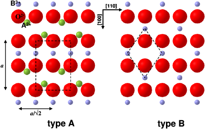
Here, we consider the surface and interface properties of [110]-oriented epitaxial films of the prototypical Co3O4 spinel grown on MgAl2O4(110) substrates. While the growth of polycrystalline Co3O4 films has been reported extensively [16, 17, 18, 19], the growth of epitaxial Co3O4 films has been studied much less often. In one instance, epitaxial Co3O4 films up to 5 Å thick have been grown on CoO(001) single crystals by oxidation at high temperatures in an oxygen atmosphere [20, 21]. Atomic layer deposition has also been used to grow epitaxial Co3O4 films on MgO(001) [19]. However, the use of MgAl2O4 substrates has several unique advantages; both materials are normal spinels and have lattice constants that match each other almost exactly, Å for Co3O4 [22] and Å for MgAl2O4 [23, 24]. The same crystal structure should also preclude the formation of antiphase boundaries that originate when lower symmetry structures are grown on higher symmetry surfaces, and the good chemical and thermal stability of MgAl2O4 guarantees no interdiffusion at high growth temperatures. The (110) surface is also characterized by having a four-repeat period as opposed to the eight-period repeat of the (100) surface, and therefore should be less susceptible to stacking faults and antiphase boundary formation, leading in principle to fewer defects in the film. As pictured in Fig. 1, in the [110]-direction the spinel structure is composed of type A planes with a CoCoO4 stoichiometry and a formal charge of +2 per surface unit cell alternating with CoO4 type B planes with a formal charge of –2. The orientation is therefore polar, and faceting or reconstruction of the film surfaces might be expected.
In this paper we show that Co3O4(110) thin films can be grown epitaxially on MgAl2O4(110) substrates by oxygen assisted molecular beam epitaxy. Despite the expectation that the polar surfaces would reconstruct, we observe only () surface diffraction patterns with no evidence of periodic reconstructions. Although the as-grown films display rough surfaces and bulk defects, these features can be largely eliminated by post-growth annealing in air, which leads to well ordered, atomically flat surfaces and interfaces. Such well defined surfaces have allowed the growth of stoichiometric epitaxial PdO thin films for surface reaction studies [25]. Interestingly, we find that annealing appears to change the surface termination from a () B-type termination to a () A-type termination. A model of the () surfaces that allows for compensation of the polar surfaces will be presented.
2 Sample growth and characterization
MgAl2O4(110) single crystals were used as substrates for the growth of Co3O4 due to the small lattice mismatch of –0.05% and good thermal and chemical stability. The substrates were first outgassed and cleaned in situ with an O-plasma at 770 K for 30 min. Such treatment renders the MgAl2O4 surface free of C contaminants, as determined by Auger electron spectroscopy (AES); the only impurities detected consist of 2-3 at. % Ca to within the probing depth of AES, about 3 nm. The high quality of the MgAl2O4(110) surface crystallinity was confirmed by low energy electron diffraction (LEED) and reflection high energy electron diffraction (RHEED), which display patterns characteristic of highly ordered surfaces (see Figs. 2 and 3). The Co3O4 films were grown by oxygen assisted molecular beam epitaxy by simultaneous exposure of the substrate to a thermally evaporated Co atomic beam and an atomic O flux. Initial growth studies indicated that better films were obtained when growth was started at 770 K and then lowered to 570 K after about 1 nm deposition, as judged by RHEED. The initial higher temperature promotes surface diffusion, while continued growth at this temperature caused CoO to form. The oxygen partial pressure during growth was mbar, and the electron cyclotron resonance oxygen plasma source magnetron was run at 125 W, yielding an atomic O flux of the order of cm-2s-1 at the sample [26, 27]. The Co evaporation rate was typically 2 Å/min, and film thicknesses were estimated by means of a calibrated quartz crystal balance. Sample growth was monitored with RHEED, and after layer completion, the Co3O4 film crystallinity and electronic structure were determined by RHEED, LEED, x-ray photoemission (XPS), and Auger electron spectroscopy (AES). AES indicates that no significant amounts of impurities were present (none were detected within the accuracy of our spectrometer, equipped with a double-pass cylinder mirror analyzer).

After film growth, the samples were characterized using a variety of structural techniques, before and after annealing, including x-ray diffraction and reflectometry, atomic force microscopy and transmission electron microscopy. Sample annealing was performed at 820 K for 14 h in flowing air; this temperature and oxygen partial pressure favor the formation of Co3O4 over CoO [28, 29, 30]. For this study, eight sets of samples were grown and characterized, and the results were found to be consistent and reproducible for all samples, in particular the LEED, RHEED, XPS, atomic force microscopy (AFM) and AES data. Non-contact AFM data were taken on two different samples, and transmission electron microscopy (TEM) measurements were made on one sample only (for TEM, one half was annealed after cleaving, for a comparative study). In the following, the LEED and RHEED data correspond to the same sample, for better comparison of the electron diffraction data.
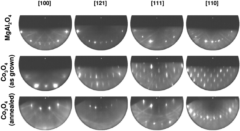
Typical LEED and RHEED patterns of the Co3O4 films after growth are shown in Figs. 2 and 3, respectively. Compared with the MgAl2O4 LEED patterns, the diffraction spots of the as-grown Co3O4 film are much broader, and the background is also more intense, indicating that the as-grown Co3O4 films have a significant amount of surface disorder (severe charging of the surface also contributes to the poor patterns, especially at lower electron beam energies). The RHEED patterns exhibit streaky and relatively broad diffraction spots, characteristic of a three dimensional growth mode and a relatively disordered surface. However, Kikuchi lines are observed along some directions (the observation of Kikuchi patterns in RHEED has been associated with the presence of relatively smooth surfaces [31]). Both RHEED and LEED data indicate that, despite the local surface disorder, long range order is preserved.
The annealing process induces significant transformations in the film structure, as indicated by different and much sharper LEED and RHEED patterns. In fact, the quality of these patterns becomes comparable to that of the MgAl2O4 single crystal substrate surface. For the annealed Co3O4 surface, the LEED background intensity is very low, with very sharp diffraction spots, and our data show that in the range from 40 eV to 150 eV there are no changes in the LEED pattern and no discernible increase in background intensity. One striking feature of the LEED patterns is the different symmetry exhibited by the as-grown and annealed films: while the former exhibit an oblique unit cell, the latter is found to exhibit predominantly a rectangular unit cell. Such LEED patterns are compatible with the two possible terminations of the (110) plane of the spinel structure: type A termination for the annealed films, exhibiting a rectangular unit cell, and type B for the as-grown films, with an oblique unit cell (see Fig. 1).
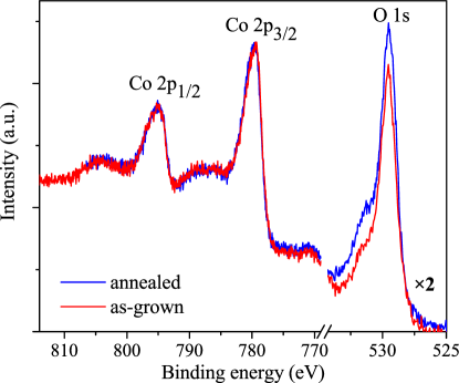
X-ray photoemission spectroscopy measurements of the Co3O4 films after growth and after annealing were carried out to assess the film stoichiometry. The XPS spectra were obtained using the Mg Kα line ( eV) of a double anode x-ray source and a double pass cylinder mirror analyzer ( 15-255G) set at a pass energy of 25 eV (energy resolution of about 0.8 eV). High resolution XPS spectra of the O 1s and Co 2p lines of the as-grown and annealed films are shown in Fig. 4. Corrections to the data include a five-point adjacent smoothing, satellite correction and correction of energy shifts due to charging (aligned with respect to the Co 2p peaks, using the energy assignments given in [32, 33]). One observation is that the Co 2p spectra for both samples are identical, showing that no significant changes in stoichiometry or in the ionic state of the Co cations occur as a consequence of annealing. A second observation is that the Co 2p spectra are characteristic of a Co3O4 ionic environment [32, 33], with strongly suppressed shake-up peaks compared to those of CoO [34, 32, 33, 30, 21, 35, 36, 37]. The O 1s photoemission line is also similar before and after annealing, although some variation in the shape of the O 1s line is observed. This could be related, in some instances, to the effect of the O-plasma cleaning procedure (at room temperature) before XPS spectra collection: given the surface sensitivity of XPS, small variations in the amount of surface adsorbed O may lead to slight variations in the O 1s line; in fact, the additional peak observed at higher binding energies has been attributed to adsorbed oxygen [32, 38, 39, 40, 41, 42, 20, 37], although surface hydroxylation, which also yields a similar peak [33, 37], cannot be ruled out.
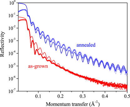
Structural characterization of the Co3O4 films was carried out ex situ by x-ray scattering measurements on a Shidmazu diffractometer using the Cu Kα line ( Å) with a Ni filter to remove the sharp Cu Kβ lines. x-ray diffraction (XRD) spectra of the as-grown and annealed films show only diffraction peaks associated with the (110) planes of MgAl2O4; this also indicates that the cobalt oxide grown is Co3O4, since only this phase has diffraction peaks that coincide with those of MgAl2O4. The spectra for the as-grown and annealed films are identical, although the diffraction lines of the Co3O4 and MgAl2O4 cannot be discriminated due to the closeness of the lattice constants of the two structures. Rocking curves of the (220) and (440) peaks show a double peak in the as-grown sample, which is attributed to the presence of twin domains in the MgAl2O4 substrate; this double peak feature is absent in the annealed sample, indicating that the MgAl2O4 domains have merged upon annealing. The full width at half maximum (FWHM) of these peaks is below the instrumental resolution of the diffractometer, 0.02o. More significant are the x-ray reflectivity (XRR) spectra for the as-grown and annealed films. In this scattering geometry, interference between the film interfaces gives rise to oscillations in the reflected intensity (Kiessig fringes), whose amplitude depends on the difference in potential between interfaces; interface roughness dampens these oscillations and affects the rate of decay in intensity with momentum transfer. Below the critical angle for total reflection, all light is reflected off the surface. The XRR spectra of as-grown and annealed Co3O4 films are shown in Fig. 5. One finds that the reflected intensity of the as-grown film falls off rapidly, with a strong dampening in the fringe oscillations, suggesting relatively rough interfaces; the annealed film, however, shows undamped oscillations over the entire momentum transfer range probed, up to 0.5 Å-1. Fits to the data were performed using bulk scattering factors and, starting with nominal thicknesses and initial guesses for the interface roughness parameters, by modifying the initial parameters until a good visual fit to the data was obtained; the accuracy of the fits are within Å for the interface roughness and Å for the thickness (which does not take into account systematic errors, such as sample displacement, which occurs if the sample is not in the center of the goniometer circle). The fits to the experimental data suggest that the interface roughness has decreased from 10-20 Å for the as-grown film to 0-2 Å after annealing; in addition, it is found that both surface and interface interface roughness parameters have changed, indicating that structural changes occur throughout the whole film following the annealing procedure.
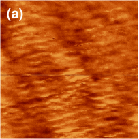
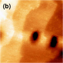
The surface morphology was also probed using real space techniques, including atomic force microscopy (AFM) at room temperature and high resolution non-contact atomic force microscopy (NC-AFM) at low temperatures. AFM in contact mode was used to obtain a large area scan of the surface morphology; these scans show that annealing induces a significant surface smoothing, with the average roughness (measured over a 4 m2 area) decreasing from 2.5 Å to 1.5 Å upon annealing. Nanometer scale topographical measurements were performed on the as-grown and annealed Co3O4 thin films using a home built, low-temperature, ultrahigh vacuum atomic force microscope, described in detail elsewhere [43]. The microscope operates in non-contact mode [44] using the frequency modulation technique [45] with a quartz tuning fork and an electrochemically etched Pt/Ir tip force sensor [46, 47]. Prior to the measurements, the sample was cleaned in the instrument preparation chamber under an oxygen plasma (at mbar pressure) at 370 K for 45 min for the as-grown sample and 3 h for the annealed sample. The results of both measurements are shown in Fig. 6 and provide striking evidence for the improvement in surface morphology upon annealing. The surface topography of the as-grown film is irregular, with elongated features set preferentially along one direction, which the RHEED data suggests to be along the in-plane [100] direction. In contrast, the annealed surface exhibits well defined atomic steps, confirming the atomic smoothness suggested by the reciprocal space techniques. Figure 6(c) shows a line profile over four terraces, spanning about 0.8 nm in height, giving a step height of 0.27 nm, which corresponds approximately to two Co3O4(110) atomic planes, 0.286 nm in height. This result confirms a single termination for the annealed films, consistent with the LEED results.

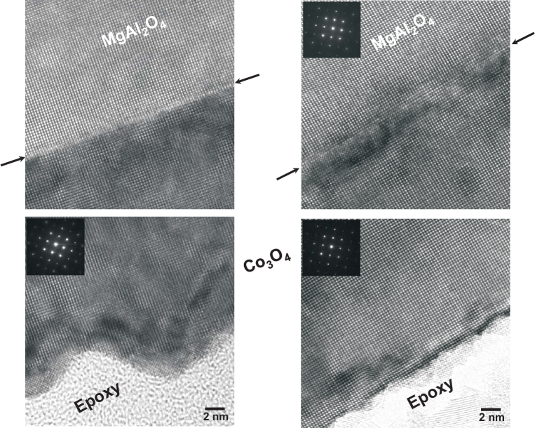
In addition to the surface characterization, we have carried out cross-sectional high resolution transmission electron microscopy (TEM) measurements in order to obtain a more detailed knowledge of the crystalline structure at the film interface and in the bulk of the film. Sample preparation involved slicing, polishing, dimpling and Ar-ion milling in a liquid nitrogen cooled sample stage. The TEM images were obtained in a JEOL 3000F microscope at 300 kV with a point resolution of 0.165 nm. Representative TEM images obtained for the as-grown and annealed samples are shown in Fig. 7, where several modifications in the film structure upon annealing are evident, both at the interface and in the bulk of the films: (i) one observes that while the Co3O4/MgAl2O4 interfaces are well defined for both the as-grown and annealed films, in the regions of 2-3 unit cells from the interfaces the details of the interfacial structure differ significantly in that the atomic positions, as represented by the white dots, seem off registry compared with the regions away from the interface for the as-grown film, suggesting the presence of interfacial strain, while little registry deviation is observed for the annealed film. (ii) In the bulk of the as-grown film, the TEM images show speckle contrast, indicating the presence of lattice distortion as well as variation in sectional thickness, which could also indicate the presence of structural disorder along the in-plane [100] direction, as suggested by the observation of the broadening of the Bragg reflections seen in the inset to Fig. 7 (top left). For the annealed film, the integrity of the crystal structure in the bulk of the film is nearly perfect. (iii) At the surface of the film, one finds that the as-grown film has a relatively large surface roughness; the clearly defined side profile indicates that the roughness is oriented along the [110] direction, as also suggested by the RHEED and NC-AFM data. The surface atomic structure of the as-grown film seems to be strongly modified at the top of the islands as compared to the bulk of the film. For the annealed film, the top surface is terminated abruptly by relatively flat plateaus, in agreement with the results of the NC-AFM measurements. From TEM images taken at lower resolutions, we observe that the Co3O4 layer thickness remains constant before and after annealing, at 25 nm, with a roughness modulation of about 3.3 nm in amplitude for the as-grown film (this is not in disagreement with the AFM roughness values: more localized probes tend to give higher roughness values due to higher spatial resolution). One effect of annealing is that of reducing drastically the surface roughness, which indicates a significant thermally activated mass transport during annealing; given the small lattice mismatch between Co3O4 and MgAl2O4, the state of lowest surface energy (area) seems to be that of thermodynamic equilibrium, while the roughening process must be kinetically set during the film growth. Overall, the TEM measurements indicate that post-growth annealing results in films that have improved crystal structure and atomically sharp and flat interfaces.
3 Discussion and conclusions
As we have shown above, the as-grown epitaxial Co3O4 films are characterized by a certain amount of disorder and by a surface atomic configuration that yields an oblique LEED pattern, consistent with a preferential termination of the Co3O4(110) surface in a B plane. On the other hand, annealing improves the bulk and interface crystalline order, smoothens the surface, and changes the termination to a Co3O4(110) A plane. The transmission-like spots in the RHEED patterns obtained during growth indicate that the film roughens as it grows. Such roughening can be a result of kinetic limitations, for example a barrier for adatoms to descend steps, or thermodynamics. Since the lattice match is essentially perfect, strain can be eliminated as a potential thermodynamic driving force for roughening, leaving surface energetics as the only viable driving force for roughening. Because the Co3O4 (110) surface is polar, the electrostatic contribution to its surface energy increases linearly with film thickness. Therefore, one can envision a growth sequence in which the film is initially flat because the electrostatic contribution to the surface energy for a film only a few layers thick is modest; as the film thickens, however, the surface energy increases until the energy is reduced by film faceting. The problem with this explanation is that the surface diffraction data indicates that the film still exposes predominantly polar (110) facets. The results, therefore, suggest that the roughening is more the result of kinetic limitations during growth than thermodynamics. The observation of the A termination of the substrate and the film after annealing, but the B termination during growth, suggests a potential kinetic limitation to forming the apparently lower energy A termination during growth.
For the B termination, where the background in the LEED patterns is high, it is possible that subsurface layers may contribute to the LEED pattern, and the broad diffraction spots, also observed in the RHEED data, suggest disorder or small domains for this surface. For the annealed surface (A termination), however, the LEED background intensity is very low, with very sharp diffraction spots. The electron mean free path is at a minimum at around 50 eV in LEED, and our data shows that in the range from 40 eV to 150 eV there are no changes in the LEED pattern and no discernible increase in the background intensity, indicating that we are probing the topmost surface layer and that the presence of a disordered surface layer can be ruled out.
Although the MgAl2O4(110) substrate, the as-grown B terminated Co3O4, and the annealed A terminated Co3O4 are all polar surfaces, only () surface diffraction patterns were observed. The divergent electrostatic surface energy of polar surfaces can be compensated in a variety of ways, including surface reconstructions, surface defects, and adsorption of polar molecules at the surface [10, 11]. Several theoretical calculations of the surface energies of the (110) surface of MgAl2O4 consider significant modifications of the bulk termination surface to remove the charge dipole, for instance by removing half the atoms in the type-A termination (Fig. 1) or considering a surface composed of O only (which yields the lowest surface energy) [48, 49, 50, 11]. These calculations also predict large surface relaxations of the surface atoms; in addition, surface inversion in the spinel structure, whereby B3+ ions swap position with A2+ ions of the layer below, also results in significantly lower surface energies [48]. The observed () LEED patterns rule out any compensation mechanism that involves a periodic surface reconstruction. While these patterns are still compatible with a modified surface composition which keeps the surface unit cell periodicity, this must be achieved while achieving charge compensation. This issue has been addressed in the literature for MgAl2O4(110) surfaces [48, 49, 50, 11], which show that charge compensation leads to large modifications to the surface composition; this would lead to larger surface unit cells, and to smaller unit cells in LEED, which is not observed. The adsorption of molecules at the surface should also be considered as a possible mechanism leading to stabilization of the A and B terminations. For example, it is now recognized that the long-range ordering of the polar (000) surface of ZnO is likely due to hydroxylation of the surface [51, 52, 53, 54]. In the present case, adsorption of H in the form of protons could screen the charge on the B-terminated surface, which would be negatively charged for the bulk termination, while water dissociation could result in OH- radicals and screen the A-terminated surface, which is positively charged for the bulk truncation. While this could explain the shoulder in the 1s O peak of the Co3O4 XPS spectra [33, 37], it is unlikely that they would give the same signature in the two cases. In fact, the shoulder is identical for both terminations, with little variation in energy and intensity for both the as-grown samples, measured immediately after growth, and for the annealed samples, which are cleaned in an O-plasma after been exposed to air (this shoulder is often assigned to adsorbed O [32, 38, 39]). Therefore, assignment of the shoulder to H on the surface cannot provide the needed screening for both surfaces. Instead, we propose that the surfaces are compensated by an ionic exchange mechanism, which in the case of Co3O4 reduces to filling and depleting surface electronic states on opposite sides of the film. An estimate of the degree of charge transfer can be obtained by assuming the formal charges on the ions. As described in the Introduction, along the [110] direction the spinel structure is composed of alternating, equally spaced A2+ and B2- planes. In this case, the thickness dependent component of the surface dipole can be eliminated by placing charges of 1 per surface unit cell on opposite sides of the crystal [10]. For the spinel, changing the stoichiometry of the two outermost layers to MgAl5O8 and Mg3Al3O8 can provide the necessary 1 charges. For Co3O4 this same charge compensation is achieved by transferring an electron from one side of the crystal to the other, thereby oxidizing one Co2+ to Co3+ on one side, and reducing one Co3+ to Co2+ on the opposite side; or in a more general picture, filling a surface state on one side and depleting it on the other. As noted by Noguera [10], more precise modeling of the charges on the ions does not appreciably change this picture. Because the electron scattering cross-sections are nearly the same for Al and Mg, and are unchanged for Co3O4, this model is consistent with the observed () diffraction patterns.
The model proposed above suggests that the A-terminated annealed surface should have a unique filled surface state that does not exist in the bulk, and may confer the surface with unique electronic and magnetic properties in a manner analogous to the metallic behavior observed for LaAlO3/SrTiO3 interfaces. We are currently further investigating this possibility using ultraviolet photoemission spectroscopy. Real space images of the atomic surface order, for instance as imaged by AFM or STM, will also be particularly useful in developing a more complete picture of the charge compensation mechanisms at work.
In summary, we have demonstrated the growth of high quality epitaxial Co3O4(110) thin films on MgAl2O4(110) by oxygen assisted molecular beam epitaxy. Post-annealing is found to improve considerably the film characteristics, as shown by several reciprocal and real space probing techniques. Two different surface terminations of the Co3O4(110) surface are observed for the as-grown and annealed films, which are associated with the two possible terminations of the bulk Co3O4(110).
Acknowledgements
The authors acknowledge financial support by the NSF through MRSEC DMR 0520495 (CRISP), MRSEC DMR 0705799, the ONR (C.H.A.), the Petroleum Research Foundation Grant Numbers 42178-AC5 (J.W. and E.I.A.) and 42259-AC5 (B.J.A. and U.D.S.), the DOE Catalysis and Chemical Transformations Program, Grant Number DOE DE-FG02-06ER15834 (M.Z.B., T.S., E.I.A. and U.D.S.).
References
- [1] H. Bizette, Ann. de Phys. 12e Ser. 1 (1946) 233.
- [2] H. Bizette, J. de Phys. et le Radium 12 (1951) 161.
- [3] C. H. L. Blanchetais, J. de Phys. et le Radium 12 (1951) 765.
- [4] W. L. Roth, Phys. Rev. 110 (1958) 1333.
- [5] C. G. Shull, W. A. Strauser, E. O. Wollan, Phys. Rev. 83 (1951) 333.
- [6] W. L. Roth, J. Phys. Chem. Solids 25 (1964) 1.
- [7] D. Scheerlink, S. Hautecler, Phys. Stat. Sol. (b) 73 (1976) 223.
- [8] W. Jauch, M. Reehuis, H. J. Bleif, F. Kubanek, P. Pattison, Phys. Rev. B 64 (2001) 052102.
- [9] P. W. Tasker, J. Phys. C: Solid State Phys. 12 (1979) 4977.
- [10] C. Noguera, J. Phys.: Condens. Matter 12 (2000) R367.
- [11] J. Goniakowski, F. Finocchi, C. Noguera, Rep. Prog. Phys. 71 (2008) 016501.
- [12] W. A. Harrison, E. A. Kraut, J. R. Waldrop, R. W. Grant, Phys. Rev. B 18 (1978) 4402.
- [13] M. Gajdardziska-Josifovska, R. Plass, M. A. Schofield, D. R. Giese, R. Sharma, J. Electron Microsc. 51 (2002) S13.
- [14] V. K. Lazarov, R. Plass, H.-C. Poon, D. K. Saldin, M. Weinert, S. A. Chambers, M. Gajdardziska-Josifovska, Phys. Rev. B 71 (2005) 115434.
- [15] U. Schwingenschlögl, C. Schuster, Europhys. Lett. 81 (2008) 17007.
- [16] K. Przybylski, W. W. Smeltzer, J. Electrochem. Soc. 128 (1981) 897.
- [17] H. Yamamoto, S. Tanaka, K. Hirao, J. Appl. Phys. 93 (2003) 4158.
- [18] M. Burriel, G. Garcia, J. Santiso, A. Abrutis, Z. Saltyte, A. Figueras, Chem. Vap. Deposition 11 (2005) 106.
- [19] M. Rooth, E. Lindahl, A. Hårsta, Chem. Vap. Deposition 12 (2006) 209.
- [20] G. A. Carson, M. H. Nassir, M. A. Langell, J. Vac. Sci. Technol. A 14 (1996) 1637.
- [21] M. A. Langell, M. D. Anderson, G. A. Carson, L. Peng, S. Smith, Phys. Rev. B 59 (1999) 4791.
- [22] J. P. Picard, G. Baud, J. P. Besse, R. Chevalier, Journal of the Less-Common Metals 75 (1980) 99.
- [23] T. Ito, A. Yoshiasa, T. Yamanaka, A. Nakatsuka, H. Maekawa, Z. Anorg. Allg. Chem. 626 (2000) 42.
- [24] J. Daams, R. Gladyshevskii, O. Shcherban, V. Dubenskyy, N. Melnichenko-Koblyuk, O. Pavlyuk, S. Stoiko, L. Sysa, Mgal2o4, in: K. C. P. Villars (Ed.), Crystal Structures of Inorganic Compounds, Vol. 43A1 of Landolt-Börnstein, New Series, Group III, Springer-Berlag, Berlin, 2004.
- [25] C. A. F. Vaz, Y.-R. Yen, M. Herdiech, J. Wang, E. I. Altman, C. H. Ahn, V. E. Henrich, Growth and characterisation of thin epitaxial PdO films Unpublished.
- [26] W. Gao, R. Klie, E. Altman, Thin Solid Films 485 (2005) 115.
- [27] R. Anton, T. Wiegner, W. Naumann, M. Liebmann, C. Klein, C. Bradley, Rev. Sci. Instrum. 71 (2000) 1177.
- [28] H. P. Tripp, B. W. King, J. American Ceramic Soc. 38 (1955) 432.
- [29] K. Koumoto, H. Yanagida, Jpn. J. Appl. Phys. 20 (1981) 445.
- [30] M. Oku, Y. Sato, Appl. Surf. Sci. 55 (1992) 37.
- [31] W. Braun, Applied RHEED, no. 154 in Springer Tracts in Modern Physics, Springer-Verlag, 1999.
- [32] T. J. Chuang, C. R. Brundle, D. W. Rice, Surf. Sci. 59 (1976) 413.
- [33] J. Haber, L. Ungier, J. Electron Spectrosc. Relat. Phenom. 12 (1977) 305.
- [34] J. P. Bonnelle, J. Grimblot, A. D’Huysser, J. Electron Spectrosc. Relat. Phenom. 7 (1975) 151.
- [35] H. A. Hagelin-Weaver, G. B. Hoflund, D. M. Minahan, G. N. Salaita, Appl. Surf. Sci. 235 (2004) 420.
- [36] H.-Q. Wang, E. I. Altman, V. E. Henrich, Phys. Rev. B 77 (2008) 085313.
- [37] S. C. Petitto, E. M. Marsh, G. A. Carson, M. A. Langell, J. Molecular Catalysis A: Chemical 281 (2008) 49.
- [38] Y. Jugnet, T. M. Duc, J. Phys. Chem. Solids 40 (1979) 29.
- [39] Y. M. Kolotyrkin, I. D. Belova, Y. E. Roginskaya, V. B. Kozhevnikov, D. S. Zakhar’in, Y. N. Venevtsev, Materials Chemistry and Physics 11 (1984) 29.
- [40] B. Klingenberg, F. Grellner, D. Borgmann, G. Wedler, Surf. Sci. 296 (1993) 374.
- [41] B. Klingenberg, F. Grellner, D. Borgmann, G. Wedler, J. Electron Spectrosc. Relat. Phenom. 71 (1995) 107.
- [42] V. M. Jiménez, A. Fernández, J. P. Espinós, A. R. González-Elipe, J. Electron Spectrosc. Relat. Phenom. 71 (1995) 61.
- [43] B. J. Albers, M. Liebmann, T. C. Schwendemann, M. Z. Baykara, M. Heyde, M. Salmeron, E. I. Altman, U. D. Schwarz, Rev. Sci. Instrum. 79 (2008) 033704.
- [44] S. Morita, R. Wiesendanger, E. Meyer (Eds.), Noncontact Atomic Force Microscopy, Springer-Verlag, Berlin, 2002.
- [45] T. R. Albrecht, P. Grütter, D. Horne, D. Rugar, J. Appl. Phys. 69 (1991) 668.
- [46] F. J. Giessibl, Appl. Phys. Lett. 76 (2000) 1470.
- [47] F. J. Giessibl, S. Hembacher, M. Herz, C. Schiller, J. Mannhart, Nanotechnology 15 (2004) S79.
- [48] M. J. Davies, S. P. Parker, G. W. Watson, J. Mater. Chem. 4 (1994) 813.
- [49] J. H. Harding, Surf. Sci. 422 (1999) 87.
- [50] C. M. Fang, S. C. Parker, G. de With, J. Am. Ceram. Soc. 83 (2000) 2082.
- [51] M. Kunat, U. Burghaus, C. Wöll, Phys. Chem. Chem. Phys. 5 (2003) 4962.
- [52] M. Kunat, S. G. Girol, U. Burghaus, C. Wöll, J. Phys. Chem. B 107 (2003) 14350.
- [53] C. Wöll, J. Phys.: Condens. Matter 16 (2004) S2981.
- [54] C. Wöll, Progr. Surf. Sci. 82 (2007) 55.