Formation of Pt induced Ge atomic nanowires on Pt/Ge(001): a DFT study.
Abstract
Pt deposited onto a Ge(001) surface gives rise to the spontaneous formation of atomic nanowires on a mixed Pt-Ge surface after high temperature annealing. We study possible structures of the mixed surface and the nanowires by total energy (density functional theory) calculations. Experimental scanning tunneling microscopy images are compared to the calculated local densities of states. On the basis of this comparison and the stability of the structures, we conclude that the formation of nanowires is driven by an increased concentration of Pt atoms in the Ge surface layers. Surprisingly, the atomic nanowires consist of Ge instead of Pt atoms.
pacs:
73.30.+y, 73.61.-Ph, 68.43.-hSelf-assembly at surfaces forms an attractive method to engineer nanostructures.Barth et al. (2005) In recent years we have seen a rapid development in techniques to grow metal atomic nanowires (NWs) on semiconductor substrates by self-assembly. NWs have been made by adsorption of metals on planar or vicinal Si and Ge surfaces, Yeom et al. (1999); Lee et al. (2005); Ahn et al. (2005); Snijders et al. (2006); Eames et al. (2006) and by metal-silicide or -germanide formation at Si or Ge surfaces.Lin et al. (1993); Yeom et al. (2005); Gurlu et al. (2003); Schafer et al. (2006); Oncel et al. (2005) From a fundamental point of view these metallic NWs show the exotic physical properties typical of (quasi) one-dimensional systems, such as Peierls-like instabilities, charge density waves and Lüttinger liquid behavior. From the perspective of applications metal NWs offer the prospect of interconnects for quantum- and nanodevices.
Recently, Gürlü et al. produced arrays of NWs by depositing Pt on a Ge(001) surface. Perfectly straight, defect free and regularly spaced NWs with a cross-section of one atom and a length of up to one micron, are formed after annealing at K.Gurlu et al. (2003) The structures are studied by scanning tunneling microscopy and spectroscopy (STM and STS), Oncel et al. (2005); van Houselt et al. (2006); Fischer et al. (2007) characterizing the electronic states around the Fermi level. However, hampered by the lack of chemical information in STM, so far only a tentative model for the atomic structure of the NWs exists.Gurlu et al. (2003) Deposition of 0.25 monolayer (ML) Pt on Ge(001) at room temperature creates a surface with a high amount of defects and no clear identification of Pt atoms.Gurlu et al. (2004) Subsequent annealing of this surface results in the formation of patches of two different structures, the so-called - and -surfaces. It has been proposed that 0.25 ML Pt is incorporated in the top surface layer of the -surface.Gurlu et al. (2003); Fischer et al. (2007) After the same annealing step, part of the -surfaces are covered with NWs. On the basis of available STM data, the wires have been tentatively identified as Pt wires.Gurlu et al. (2003); Fischer et al. (2007)
In this paper we present a computational study of the structure of the -surface and the NWs at the first-principles density functional theory (DFT) level.com By calculating total energies and comparing simulated to experimental STM images we identify the most probable structures.sim The -terrace has a structure that is similar to the clean Ge(001) surface, but with one in four Ge atoms replaced by a Pt atom. The process of the formation of NWs is driven by an increase in the concentration of Pt in the surface layers. Most remarkably, we predict that the NWs that are observed in STM in fact consist of Ge atoms that are displaced from the substrate.
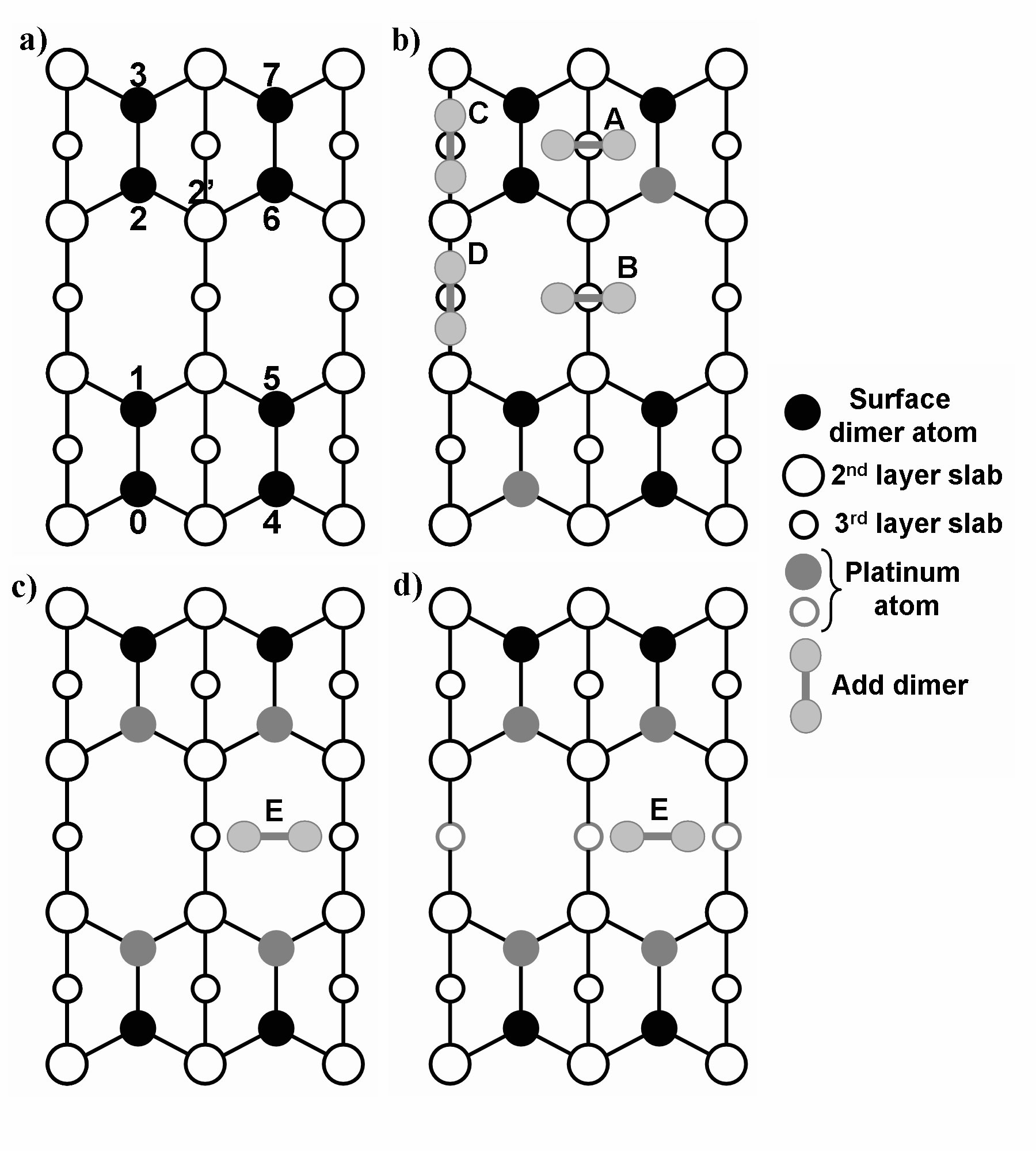
Before discussing the structure of NWs, we study possible geometries of the -surface. From STM images one can conclude that the latter has a basic structure similar to that of the clean Ge(001) surface. The top surface layer consists of rows of dimers, as shown schematically in Fig. 1(a). Compared to a clean Ge(001) surface with reconstruction, the surface unit cell of the -terrace is doubled, leading to a periodicity.Gurlu et al. (2003) Based upon the pattern observed in STM, it has been proposed that the top surface layer of the -surface contains 0.25 ML of Pt.Gurlu et al. (2003)
We calculate the total energies of possible -surface structures by replacing one in four Ge atoms in the top surface layer of Ge(001) by Pt atoms. All possible arrangements of Pt atoms in a cell are considered, see Fig. 1(a). The cell contains two Pt atoms; the first is placed at position 0, and the second platinum atom at one of the positions 1-7. We use to indicate the structure with the second atom at position . After relaxing the geometries, surface formation energies , normalized per unit cell, are calculated from
| (1) |
and are the total energies of the slabs representing the surface containing Pt atoms and the clean Ge(001) surface.fac is the number of Pt atoms and is the difference between the slabs in the number of Ge atoms; , are the energies per atom of bulk Pt and Ge. Positive/negative values of indicate that the surface is unstable/stable with respect to phase separation into Ge(001) and bulk Pt. As we will see below, Pt has a tendency to be incorporated in the Ge-surface forming Pt-Ge bonds. Moreover, surfaces with low Pt density tend to be unstable with respect to phase separation into Ge(001) and surfaces with high Pt content.
The structure, with Pt in adjacent positions (0,1), has a large positive formation energy of eV. It indicates that formation of Pt-Pt dimers is very unfavorable. In contrast, several structures with mixed Pt-Ge dimers have a negative formation energy. The most stable structure is the geometry (Pt at positions and ) having a formation energy meV. This structure consists of alternating rows of Ge-Ge and Pt-Ge dimers with all Pt atoms at the same side of a row, leading to a periodicity. The second most stable structure is the geometry (Pt at positions and ) with meV. The structure gives a checkerboard pattern of Pt-Ge and Ge-Ge dimers with periodicity.
Several geometries with mixed Pt-Ge dimers are close in energy, which means that they are thermodynamically accessible at the formation temperature of the -surface (1050K). The energy difference between the and the structures is only meV per Pt atom, for example. Studying the formation kinetics is beyond the present calculations. To identify which of the structures may explain the experimental STM results, we calculate STM images within the Tersoff-Hamann approach.sim Comparison to experimental data shows good agreement for the structure only. Other structures can be ruled out as they lead to a different periodicity or qualitatively different STM patterns.
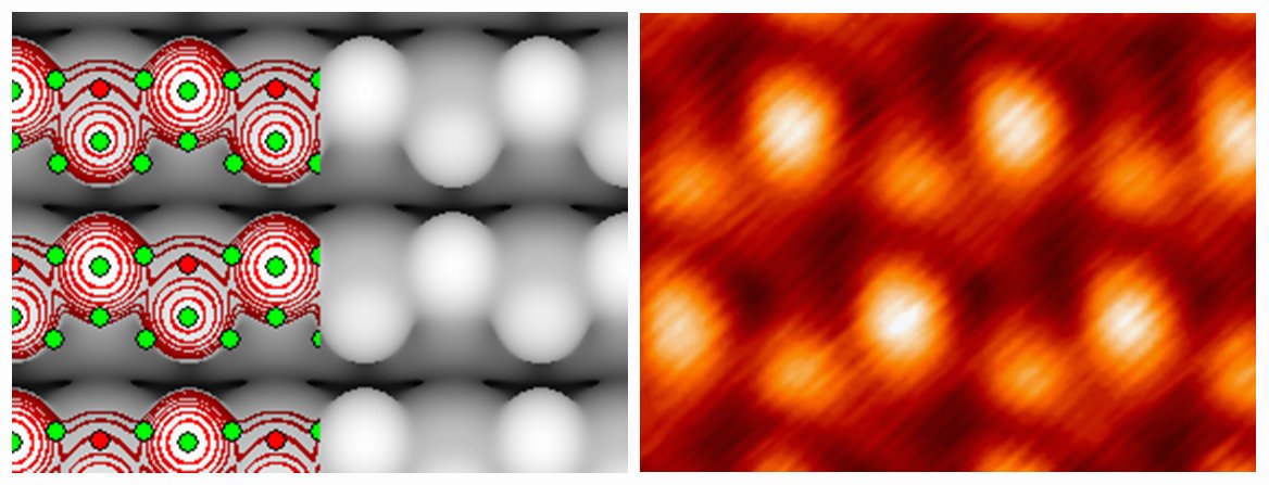
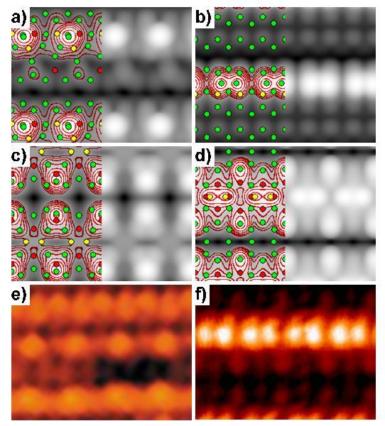
Experimentally NWs are always found on patches of -surface.Gurlu et al. (2003); Fischer et al. (2007) In addition, the NWs are clearly composed of ad-dimers. Therefore, as a first scenario we study the structure as a template for the adsorption of Pt ad-dimers. Some possible geometries are sketched in Fig. 1(b). Remarkably, none of the structures seem to be stable and optimizing the geometries can lead to large displacements of adsorbed atoms and of atoms in the substrate. For instance, the formation energies of the optimized structures resulting from initial adsorption of Pt dimers at A,B,C,D sites are eV, respectively. Although the B structure seems to be favorable, inspection of the optimized geometry shows that it is completely different from the initial adsorption of a Pt dimer at a B site. The adsorbed Pt dimer breaks up into two atoms. One Pt atom remains in the trough between the dimer rows, but sinks into the surface to form bonds with nearby Ge atoms. The second Pt atom is exchanged with the Ge atom at position 2 in the surface. The displaced Ge atom is pushed out of the surface above position (cf. Fig. 1 (a)). The reordering of Pt and Ge atoms at the surface again indicates that the formation of Pt-Ge bonds is energetically strongly favored. The displaced Ge atom forms the highest point on the surface and is the most prominent feature in the simulated filled state STM image. The pattern however does not resemble that of a NW, compare Figs. 3(a) and (f).
In a second possible scenario the Pt atoms comprising a NW are kicked out from a -surface, whereby the latter is transformed back into a Ge(001) surface. To investigate this scenario we calculate the geometries and energies of Pt dimers adsorbed on a clean Ge(001) surface. None of the structures turn out to be stable, and often lead large atomic displacements in the substrate. For example, the formation energies of the optimized structures starting from the A,B,C,D configurations, are eV, respectively. None of the simulated STM images correspond to what is observed experimentally. Fig. 3(b) shows the optimized B configuration. Remarkably, the bright features belong to Ge atoms that are displaced from the substrate; the Pt atoms remain invisible.
In conclusion, the scenario’s discussed in the previous two paragraphs are unlikely. Pt adatoms do not form a NW, but instead show a tendency to be embedded in the surface and form additional Pt-Ge bonds. The next logical step therefore is to consider a substrate where all dimers in the surface top layer are Pt-Ge dimers. Structures with the Pt atoms on the same side of a Pt-Ge dimer row are the most stable. The formation energy of the structure shown in Fig. 1(c) is eV, demonstrating that energetically this structure is reasonable. We call this structure the -surface; it consists of Pt-Ge dimers with Pt atoms at positions 1,2,5,6. The Pt-Ge dimers form rows along the horizontal direction in Fig. 1(c), not unlike the dimer rows on the clean Ge(001) surface. There are two kinds of troughs above the atoms in the third layer. The first kind is lined with Pt atoms in the surface top layer and the second kind with Ge atoms.gam The two kinds alternate on the surface, which gives a periodicity. The spacing between two troughs of the same kind is then 16 Å, which corresponds to the spacing between the NWs observed in experiment.
We use the -surface as a template to adsorb Pt or Ge dimers. Of the many possible adsorption sites we have studied, only the structure labeled E in 1(c) gives rise to NWs that can match the experiment.gam The formation energy is substantial, i.e. eV for Pt and Ge NWs, respectively. The large formation energy for Ge NWs can immediately be attributed to the formation of Pt-Ge bonds with the Pt atoms in the surface, which is energetically advantageous. The large formation energy for Pt NWs might be surprising at first sight, since the formation of Pt-Pt bonds was avoided before (see the discussion above). However, examination of the optimized structure shows that the Pt NW has in fact sunken into the through, so that the Pt atoms of the NW are Å below the average level of the atoms in the surface top layer. In fact, these Pt atoms make bonds with Ge atoms in the second and third layer, which explains the stability of the structure.
The same does not happen to a Ge NW. The Ge atoms remain at a height of Å above the average height of atoms in the surface top layer. The simulated STM image of a Ge NW is reasonably close to the experimental image with bright features at the position of the NW. However these features are not double peaked as experimentally observed for the NWs (Fig. 3(f)). Moreover, the structure of a Ge NW adsorbed on a -surface contains the same number of Pt atoms as the structure shown in Fig. 3(a). Yet its formation energy is not as favorable, which makes it a metastable structure.
The Pt NW has a low energy, but its simulated STM image, as shown in Fig. 3(c), strongly deviates from the experimental STM image. In fact, in the simulated image the Pt NW is not visible at all. This is partly due to the fact that the Pt NW has sunk into the surface, but also because Pt atoms do not give rise to a LDOS close to the Fermi level that emerges from the surface. The bright features in Fig. 3(c) correspond to Ge atoms of the surface top layer. These Ge atoms belong to Pt-Ge dimers that become strongly tilted after adsorption of the Pt NW. The tilting angle of these dimers is , whereas the tilting angle of Pt-Ge dimers on the clean -surface is . The tilting is accompanied by an increase of the Pt-Ge bond length to 2.64 Å, as compared to 2.35 Å in the -surface. The Pt atoms of the tilted Pt-Ge dimers go subsurface to form extra Pt-Ge bonds, whereas the Ge atoms stick out of the surface and give rise to bright features. The simulated image of the Pt NW shows in fact a remarkable resemblance to the wide troughs observed in Ref. Fischer et al., 2007, suggesting that these features indeed involve subsurface Pt. Note that in our structure only every other Pt-Ge dimer along a dimer row is tilted, doubling the periodicity along the row compared to the -surface to , as is observed experimentally, see Fig.3(e).Fischer et al. (2007)
We have seen that it is energetically advantageous to incorporate Pt adatoms in a trough in the -surface. One can therefore imagine the following scenario. Let the Pt atoms sink into the trough and exchange with Ge atoms in the third layer of the substrate, as indicated schematically in Fig. 1(d). We call this the -surface. The displaced Ge atoms are then pushed up from the trough and can form a NW on top with atoms in the E positions. The calculated height of these Ge NWs is Å above the surface, which is in fair agreement with the corrugation deduced from STM line scans.Zandvliet All Pt atoms in this scenario form bonds with neighboring Ge atoms, and the formation of Pt-Pt bonds is avoided altogether. The resulting structure is energetically very favorable with a formation energy eV. The exchange that is required between Pt and Ge atoms in the third surface layer might explain the high annealing temperature ( K) that is needed to form the NWs experimentally. As a check we have also replaced the Ge NW by a Pt nanowire, which leads to a substantially less favorable formation energy eV.
The simulated STM image of a Ge NW on a -surface is shown in Fig. 3(d). It is in very good agreement with the experimental STM image of Fig. 3(f). All the features of the experimental image are present in the simulated one, including the double peak structure associated with each dimer of the Ge NW and the bright features that are arranged symmetrically alongside the NW. The latter result from Ge atoms belonging to Pt-Ge dimers in the surface top layer, whereas the Pt atoms remain “invisible”. Replacing the Ge NW by a Pt NW completely removes the NW in the simulated image, which clearly indicates that the NW consists of Ge dimers. The Ge-Ge bond length of the NW dimers is 2.72 Å, which is somewhat larger than the typical bond length of 2.45 Å of a Ge-Ge dimer on the clean Ge(001) surface.
In conclusion, we have studied possible structures of the Pt-Ge surface that emerge after deposition of Pt on the Ge(001) surface. The experimentally observed -surface has ML of Pt in its top layer, which consists of Pt-Ge and Ge-Ge dimers arranged in a checkerboard pattern. Starting from either the -surface, or the clean Ge(001) surface, we find that Pt NWs are unstable structures. Pt atoms have a tendency to be incorporated in the substrate and form additional Pt-Ge bonds. We propose the -structure, which contains ML of Pt in the surface top layer, as a template for NWs. It consists of rows of Pt-Ge dimers in the top layer resulting in periodicity. The trough between the rows lined up with Pt atoms is the most favorable adsorption site for NWs. Adsorbing a Pt NW we observe that it sinks into the surface and increases the width of the trough in the STM image. Exchanging the “sunken” Pt atoms with Ge atoms in the third layer of the substrate leads to a Ge NW. This structure has a favorable formation energy and gives simulated images in agreement with the experimental STM images.
We thank Harold Zandvliet and Arie van Houselt for stimulating discussions and for making available their experimental STM results. This work is part of the research program of the “Stichting voor Fundamenteel Onderzoek der Materie” (FOM); the use of superconmputer facilities is sponsored by the “Stichting Nationale Computer Faciliteiten” (NCF), both financially supported by the “Nederlandse Organisatie voor Wetenschappelijk Onderzoek” (NWO).
References
- Barth et al. (2005) J. V. Barth, G. Constantini, and K. Kern, Nature 437, 671 (2005), and references therein.
- Yeom et al. (1999) H. W. Yeom, S. Takeda, E. Rotenberg, I. Matsuda, K. Horikoshi, J. Schaefer, C. M. Lee, S. D. Kevan, T. Ohta, T. Nagao, et al., Phys. Rev. Lett. 82, 4898 (1999).
- Lee et al. (2005) G. Lee, J. Guo, and E. W. Plummer, Phys. Rev. Lett. 95, 116103 (2005).
- Ahn et al. (2005) J. R. Ahn, P. G. Kang, K. D. Ryang, and H. W. Yeom, Phys. Rev. Lett. 95, 196402 (2005).
- Snijders et al. (2006) P. C. Snijders, S. Rogge, and H. H. Weitering, Phys. Rev. Lett. 96, 076801 (2006).
- Eames et al. (2006) C. Eames, C. Bonet, M. I. J. Probert, S. P. Tear, and E. W. Perkins, Phys. Rev. B 74, 193318 (2006).
- Lin et al. (1993) X. F. Lin, K. J. Wan, J. C. Glueckstein, and J. Nogami, Phys. Rev. B 47, 3671 (1993).
- Yeom et al. (2005) H. W. Yeom, Y. K. Kim, E. Y. Lee, K.-D. Ryang, and P. G. Kang, Phys. Rev. Lett. 95, 205504 (2005).
- Gurlu et al. (2003) O. Gurlu, O. A. O. Adam, H. J. W. Zandvliet, and B. Poelsema, Appl. Phys. Lett. 83, 4610 (2003).
- Schafer et al. (2006) J. Schafer, D. Schrupp, M. Preisinger, and R. Claessen, Phys. Rev. B 74, 041404(R) (2006).
- Oncel et al. (2005) N. Oncel, A. van Houselt, J. Huijben, A. S. Hallback, O. Gurlu, H. J. W. Zandvliet, and B. Poelsema, Phys. Rev. Lett. 95, 116801 (2005).
- van Houselt et al. (2006) A. van Houselt, N. Oncel, B. Poelsema, and H. Zandvliet, Nano Letters 6, 1439 (2006).
- Fischer et al. (2007) M. Fischer, A. van Houselt, D. Kockmann, B. Poelsema, and H. J. W. Zandvliet, Phys. Rev. B 76, 245429 (2007).
- Gurlu et al. (2004) O. Gurlu, H. J. W. Zandvliet, B. Poelsema, S. Dag, and S. Ciraci, Phys. Rev. B 70, 085312 (2004).
- (15) We use a plane wave basis set and the PAW formalism Blöchl (1994); Kresse and Joubert (1999) at the level of the local density approximation, as implemented in the VASP code.Kresse and Hafner (1993); Kresse and Furthmüller (1996) The plane wave kinetic energy cutoff is set at 345 eV. The supercell contains a symmetric slab of 12 layers of Ge atoms. Pt atoms are added or replace Ge atoms on both (top and bottom) surfaces. A vacuum region of Å separates the periodic images of the slab. We use a k-point grid to sample the Brillouin zone of the surface unit cell. To optimize the geometry we apply the conjugate gradient algorithm while keeping the positions of the germanium atoms in the center two layers fixed at their bulk positions.
- (16) The Tersoff-Hamann model is used, in which tunneling currents are represented by integrating the local density of states (LDOS) of the surface over a range that corresponds to the applied bias .Tersoff and Hamann (1985) We mimic the STM constant current mode by tracing a constant integrated LDOS as a function of and mapping on a grayscale. At the position of the highest atom Å.
- (17) Dividing the number by two, since our slabs contain two identical surfaces at the top and bottom.
- (18) H. J. W. Zandvliet, unpublished.
- (19) We have also studied other structures corresponding to 0.5ML of Pt in the surface and Pt or Ge nanowires adsorbed at different positions. None of these lead to strucures that resemble the experimental STM images.
- Blöchl (1994) P. E. Blöchl, Phys. Rev. B 50, 17953 (1994).
- Kresse and Joubert (1999) G. Kresse and D. Joubert, Phys. Rev. B 59, 1758 (1999).
- Kresse and Hafner (1993) G. Kresse and J. Hafner, Phys. Rev. B 47, (R)558 (1993).
- Kresse and Furthmüller (1996) G. Kresse and J. Furthmüller, Phys. Rev. B 54, 11169 (1996).
- Tersoff and Hamann (1985) J. Tersoff and D. R. Hamann, Phys. Rev. B 31, 805 (1985).