Radiation Tolerance of Fully-Depleted P-Channel CCDs Designed for the SNAP Satellite
Abstract
Thick, fully depleted p-channel charge-coupled devices (CCDs) have been developed at the Lawrence Berkeley National Laboratory (LBNL). These CCDs have several advantages over conventional thin, n-channel CCDs, including enhanced quantum efficiency and reduced fringing at near-infrared wavelengths and improved radiation tolerance. Here we report results from the irradiation of CCDs with 12.5 and 55 MeV protons at the LBNL 88-Inch Cyclotron and with 0.1 - 1 MeV electrons at the LBNL 60Co source. These studies indicate that the LBNL CCDs perform well after irradiation, even in the parameters in which significant degradation is observed in other CCDs: charge transfer efficiency, dark current, and isolated hot pixels. Modeling the radiation exposure over a six-year mission lifetime with no annealing, we expect an increase in dark current of 20 e-/pixel/hr, and a degradation of charge transfer efficiency in the parallel direction of and in the serial direction. The dark current is observed to improve with an annealing cycle, while the parallel CTE is relatively unaffected and the serial CTE is somewhat degraded. As expected, the radiation tolerance of the p-channel LBNL CCDs is significantly improved over the conventional n-channel CCDs that are currently employed in space-based telescopes such as the Hubble Space Telescope.
Index Terms:
Astrophysics and Space Instrumentation, Radiation Damage EffectsI Introduction
The SuperNova/Acceleration Probe (SNAP) is a proposed space-based telescope dedicated to the study of dark energy through the observations of Type Ia supernovae (Ia SNe) and a deep, wide area weak lensing survey[1]. From its orbit at the second Earth-Sun Lagrange point (L2), SNAP will carry out two surveys: a deep survey of square degree field with 4-day cadence repeat visits over a period of 22 months to discover and obtain light curves and spectra of over 2000 Ia SNe in the redshift range ; and a wide area weak lensing map to study the growth of large scale structure that will cover 1000 square degrees per year to a depth of AB magnitude in the optical filters. In an extended 6 year SNAP mission, the weak lensing survey covers 4000 square degrees and the mission lifetime.
The telescope is designed with a square degree instrumented field of view divided evenly between 36 CCDs and 36 HgCdTe detectors. The SNAP observing strategy implements a four-point dither pattern with an exposure time of 300 seconds to recover spatial information from the undersampled optics and to reject cosmic rays. The focal plane will be passively cooled to 140 K. Nine fixed filters cover the wavelength range 400 nm to 1700 nm. With a diffraction limited point spread function (PSF) of arcseconds at 800 nm and zodiacal-dominated background, SNAP will have significantly improved resolution and decreased contamination from sky background compared to ground based telescopes.
The SNAP focal plane design uses thick, fully depleted CCDs developed at LBNL [2, 3] for visible to near IR observations in six bandpass filters. In space, these detectors will be exposed to significant radiation, primarily solar protons. In this paper we investigate the effects of six years of radiation at L2 on SNAP CCDs in order to qualify them for use in a space mission. In §II we describe the SNAP CCDs and the specifications for performance. The space environment and expected radiation exposure are discussed in §III. Irradiation using the 88-Inch Cyclotron and the 60Co source at LBNL is described in §IV and §VI respectively. CCD performance after proton irradiation is reported in §V and after 60Co irradiation in §VII. Finally, we present an interpretation of the results in the context of the SNAP mission in §VIII and the conclusions in §IX.
II CCD Requirements
| Quantity | Requirement | Achieved (pre-irradiation) |
| Wavelength Coverage | nm | nm |
| Quantum | at nm | at nm |
| Efficiency | at 1000 nm | at 1000 nm |
| Readout Time | 30 seconds | 30 seconds |
| Read Noise | 6 e- | 4 e- |
| Diffusion (RMS) | m | m |
| Defect Pixelsa | To Be Determined | |
| Dark Currenta | 100 e-/hr | e-/hr |
| Serial CTEa | To Be Determined | 0.999 999 |
| Parallel CTEa | To Be Determined | 0.999 999 |
| aexpected to deteriorate with irradiation | ||
SNAP CCDs have been designed for back-illumination on 200 m thick, fully-depleted, high-resistivity silicon. A factor of ten increase in thickness over conventional CCDs provides vastly improved sensitivity toward wavelengths of m and negligible fringing effects caused by multiple reflections in the silicon[4, 5]. The CCDs are depleted through application of a substrate bias voltage across the full thickness. The spatial resolution can be improved by increasing the bias voltage up to 200 V[3], with a nominal operating voltage of 100 V for the SNAP mission. The SNAP focal plane will be populated with 36 LBNL CCDs, each having m pixels.
The objectives of the SNAP experiment are to extract point-source SNe from diffuse host galaxies and to resolve distant galaxies for weak lensing studies. The specifications for CCD performance are therefore governed by requirements for preservation of the point spread function (PSF), high quantum efficiency (QE), charge transfer efficiency (CTE) and signal-to-noise ratio. In Table I we list the specifications for the SNAP CCDs. As can been seen in the table, each of these requirements has been met in the current design of SNAP style devices before radiation exposure.
CCD performance is expected to degrade in a radiation environment due to bulk damage from non-ionizing energy loss (NIEL) and due to charging of oxide layers from ionizing radiation. The major bulk damage in conventional n-channel CCDs is caused by traps generated in the formation of phosphorus-vacancy centers[6]. This bulk damage manifests itself through decreased charge transfer efficiency, increased dark current, and isolated hot pixels. The LBNL p-channel CCDs are fabricated on high-resistivity n-type silicon with boron implanted channels. In the p-channel CCDs, divacancy states are expected to be the dominant hole trap [7, 8, 9]. It has been predicted that divacancy formation in p-channel CCDs is less favorable than phosphorus-vacancy traps in n-channel CCDs [8], and prior studies have shown improved performance after radiation exposure [7, 10, 11].
Ionizing radiation is expected to result in charging of oxide layers, requiring adjustment of pixel gate voltages and output source follower transistor biasing. Significant increases in dark current after ionizing radiation have also been observed in p-channel CCDs[8]. In this work we investigate the effects of both kinds of radiation damage on SNAP CCDs, focusing on generation of dark current, hot pixels, and decrease in charge transfer efficiency.
III Space Environment and Expected Dose
The SNAP satellite will orbit at the L2 Lagrange point, approximately km from Earth. At this distance, solar protons dominate the total radiation dose. To estimate the total exposure at L2, we use the Emission of Solar Protons (ESP) model described in [12] and the Space Environment Information System (SPENVIS)[13]. In SPENVIS, the solar model is simplified as a cycle with seven years at maximum activity with constant exposure and four years at minimum activity with no exposure. The model provides a statistical estimate of the fluence as a function of confidence interval based on data from the past three solar cycles. A simple shielding model is used in which a spherical aluminum shell surrounds the detectors. The propagation of particles through the shielding is also simplified; showers and secondary particles are not modeled. With these simplifications, we make a first-order estimate of the effects of radiation on the SNAP visible detectors. A more detailed Monte Carlo simulation of the propagation of particles through the structures of the satellite will be performed at a later date.
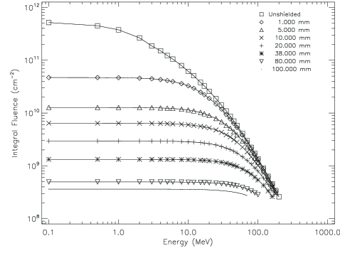
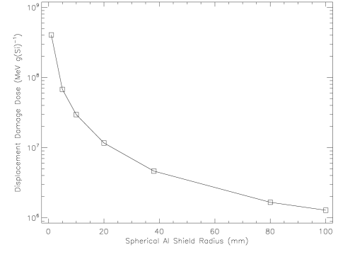
Assuming a six year extended mission with a January 1, 2014 launch date, we estimate the accumulated radiation exposure for the SNAP CCDs at the confidence level. Figure 1 shows the spectrum of protons incident on the detectors for various shield thicknesses predicted by ESP and SPENVIS. Similarly, Figure 2 reports the integrated non-ionizing energy loss (NIEL) as a function of shield thickness.
| Device | Format | Radiation | Energy | Warm/Cold | Dose |
|---|---|---|---|---|---|
| 1 | pixels, FI | proton | 55 MeV | warm | , , , protons/cm2 |
| 3 | pixels, BI | proton | 12.5 MeV | warm | , , , protons/cm2 |
| 4 | pixels, FI | proton | 12.5 MeV | cold | , , protons/cm2 |
| 5 | pixels, FI | proton | 12.5 MeV | warm | protons/cm2 |
| 6 | pixels, FI | proton | 12.5 MeV | warm | protons/cm2 |
| 7 | pixels, FI | proton | 12.5 MeV | warm | protons/cm2 |
| 8 | pixels, FI | proton | 12.5 MeV | warm | protons/cm2 |
| 9 | pixels, FI | electron | 0.1 - 1.0 MeV | cold | 1.2 krad |
Analysis of the satellite mechanical structure shows the detector shielding thickness varies by almost a full order of magnitude over the full range of angles of incidence. The distribution of the material surrounding the focal plane over is shown in Figure 3. The present satellite design provides an average shielding equivalent to about 47 mm of Al shielding around the focal plane, with a minimum of 9 mm of Al equivalent over a small fraction of the solid angle. The SNAP satellite has not yet been fully optimized for radiation shielding, and future modifications can provide additional shielding in the thinnest regions, so our current estimates may be considered conservative.
We have computed the average NIEL at the SNAP focal plane by folding the expected NIEL at L2 as a function of shield thickness with the distribution of shielding thickness in the current SNAP design. We find an integrated NIEL dose of MeV/g (Si). Assuming a NIEL damage factor of Mev/g/cm2 for MeV protons[14], this is equivalent to a dose of 12.5 MeV protons/cm2. We report results of the radiation tolerance of the SNAP CCDs treating this dose as a “nominal” value that will be experienced by the SNAP CCDs at CL after six years at L2.

IV Irradiation at the LBNL 88-Inch Cyclotron
Nine CCDs were characterized before irradiation, with performance very similar to that described in Table I. Charge transfer efficiency (CTE) was measured using the 55Fe 5.9 keV line [11] for both parallel and serial transfers. Gain conversion from ADC count (ADU) to e- was also determined using 55Fe images. Dark current was determined from the mean signal in 10 minute dark exposures, after removal of 3 outliers to account for cosmic ray contamination. Ten dark images were taken successively and median-combined to generate a high signal-to-noise dark image, free of cosmic rays and terrestrial background radiation. Residual hot pixels caused by a clustering of mid-level traps were identified as high significance peaks in this median-combined image. Very rarely was even a single individual hot pixel identified in a dark image at 133 K. More common were manufacturing defects, the occasional hot column caused by a minor clock short or back-side defect. For a more detailed account of clock shorts and back-side defects, see [15].
To simulate radiation exposure in the space environment, CCDs 1-8 listed in Table II were exposed at the LBNL 88-Inch Cyclotron for irradiation to 12.5 and 55 MeV protons. For convenience, most of the radiation exposures were carried out at room temperature on CCDs with all of the inputs shorted together and no bias voltages present. The proton fluence was continuously monitored during irradiation using standard ion chamber dosimetry.
To check whether warm irradiation gives the same results as irradiation at cryogenic temperatures, a full-size SNAP CCD was irradiated in a dewar at 133 K at nominal bias and clocking voltages and continuous readout at 70 kHz during the exposure. A brass shield inside the dewar could be moved into three different positions, resulting in exposures to three different regions of the CCD. The cold-irradiated CCDs allowed us to study the time evolution of the dark current, and the rate at which hot pixels were generated. In the warm-irradiated devices, both dark current and hot pixels quickly annealed at room temperature, so only the cold-irradiated CCDs could give an indication of the long-term effects. In addition, we carried out controlled periods of warming on the cold-irradiated devices to study the effects of annealing.


V Results of Proton Irradiation
Measurements on the warm-irradiated devices were made beginning four weeks after irradiation to allow the dark current to decay to a low level. Otherwise, the abnormally high dark current would mitigate the effects of degraded CTE by filling the defects created during irradiation. After this cooling off period, the CCDs were again characterized as described above to determine of the CTE as a function of dose and energy.
For CTE measurements, the 55Fe linear density was approximately one x-ray per 80 pixels for devices 1-3 and devices 5-8. The density was approximately one x-ray per 270 pixels for devices 4 and 9. All CTE measurements were carried out at a temperature of 133 K at a pixel readout rate of 70 kHz. Because of the delay between parallel transfers as each row is serially read one pixel at a time, charge is transfered about three orders of magnitude faster in the serial (line) direction than in the direction of parallel (row) transfer. The traps are most efficient when the transfer rate is comparable to the de-trapping time constant.
The cold, proton-irradiated device 4 was maintained at 133 K for seven weeks following irradiation. Dark and 55Fe images were collected on a regular basis, beginning three days after the irradiation. The primary purpose of the cold-irradiation and analysis was to determine the evolution of CTE, dark current, and isolated hot pixels at normal operating conditions over an extended period. After seven weeks, the device was allowed to anneal to room temperature for a period of 12 hours and then cooled back down to 133 K for CTE and dark current measurements. Measurements were again taken daily for another seven weeks. Comparison of the CCD performance before and after warming provide data on the effects of annealing, an analysis not possible with the warm-irradiated CCDs.
V-A Comparison of CTE on front- and back-illuminated CCDs
Most of the irradiated devices were 650 m thick, front-illuminated (FI) CCDs. Front-illumination refers to the light impinging on the front, or patterned, side of the CCD (CCDs used for astronomy are always back-illuminated for improved quantum efficiency). The FI devices lend themselves to CTE testing since 55Fe x-rays are deposited directly on the pixels, without the lateral charge diffusion that occurs in back-illuminated (BI) devices. One 200 m thick, BI SNAP device (device 3) was irradiated for comparison. CTE was measured on the irradiated BI device using the extended pixel edge response (EPER) and first pixel response (FPR) techniques [18], instead of x-rays. A detailed comparison of the BI device 3 with FI device 2 with EPER and FPR showed a similar degradation of CTE with dose. From this we conclude that the use of 650 m thick, front-illuminated devices for the study of CTE degradation with dose is a reasonable substitution for 200 m thick, back-illuminated devices.
V-B Energy Dependence of CTE Degradation
To test the validity of the NIEL scaling for CTE degradation, a SNAP CCD irradiated at 55 MeV was compared to a SNAP CCD irradiated at 12.5 MeV (devices 1 and 2 in Table II). As can be seen in Table III, the damage factor describing serial charge transfer inefficiency (CTICTE) is nearly identical for both energies, well within the uncertainty of the measurement. The damage factor was observed to be larger in parallel CTE in the case of the 55 MeV irradiation, a relatively minor difference of .
| Energy | Transfer | CTI | NIEL | Damage Factor |
| (MeV) | Direction | MeV/g (Si) | CTI/Dose/NIEL | |
| 12.5 | parallel | |||
| 55 | parallel | |||
| 12.5 | serial | |||
| 55 | serial |
V-C Scaling of CTE with Dose


| Measurement | (s) | (s) | ||
|---|---|---|---|---|
| Parallel - pre-anneal | ||||
| Parallel - post-anneal | ||||
| Serial - pre-anneal | ||||
| Serial - post-anneal |
The irradiated devices included both full-size pixel SNAP CCDs and ”mini-SNAP” CCDs of smaller format pixels but of otherwise identical design. With the use of a brass shield, the four quadrants of the full-size SNAP CCDs were individually exposed to doses of , , and protons/cm2; the mini-SNAP devices each received a single uniform dose. Comparison of the results for device 2 with devices 5, 6, 7, and 8 (Figures 4(a) and 4(b)) indicates that the radiation damage effects observed on the mini-SNAP CCDs were consistent with those observed on the full-size SNAP CCDs, thus validating the use of small-format devices of otherwise identical design for radiation studies.
The CTE of devices 2, 4, and 5-8 was analyzed and compared over the full range of exposure levels. Results of the degradation of parallel CTE are shown in Figure 4(a). There is a slight difference in the parallel CTE among the different radiation exposure conditions. This may be due to differences in the level of dark current, which can account for changes on the order of a few in CTE at a dose of protons/cm2, as discussed in §V-E. The background from dark current in the cold-irradiated device before the anneal was typically e-/pix, while the background in the warm-irradiated devices and in device 4 after annealing was typically e-/pix.
For comparison, we also include the results of CTE testing on conventional n-channel CCDs from e2v [10] in Figure 4(a). The n-channel CCDs are intended to be used in the Wide Field Camera 3 (WFC3) on the Hubble Space Telescope (HST) and were irradiated using 63 MeV protons with a fluence of protons/cm2 and protons/cm2, equivalent to 2.5 and 5.0 years in the HST orbit. Assuming a NIEL of MeV/g (Si) for 63 MeV protons[14], the equivalent dose at 12.5 MeV is protons/cm2 and protons/cm2.
Serial CTE vs dose is shown in Figure 4(b). As can be seen in the figure, the warm-up to room temperature resulted in a decrease in the serial CTE, an effect referred to as ”reverse annealing.” We also observe a significantly worse serial CTE performance in the warm-irradiated CCDs, compared to the cold-irradiated device both before and after annealing. It has been demonstrated that irradiation produces only negligible degradation of serial CTE in the n-channel e2v devices [16] and results are not included here.
V-D Effect of Annealing on CTE
| Measurement | (e-/pixel) | (events/pixel) | C | ||
|---|---|---|---|---|---|
| Parallel | |||||
| Serial |
Reverse annealing has also been observed in the n-channel CCDs used in the Chandra telescope. Following that analysis [17], we analyze the de-trapping time constants before and after annealing by computing the average signal in the pixels following the main charge packet in the 55Fe images from the cold, proton-irradiated device 4.
Each x-ray event is identified, centroided in pixel box, and included in the analysis if the center position is within pixels of the center pixel. This selection rejects events in which the x-ray is deposited near a pixel boundary. The charge is counted in each trailing pixel as a fraction of the charge in the primary charge packet for the parallel or serial directions. We then divide the trail of charge of each event by the total number of transfers and average the results. In other words, the averaged trails represent the fraction of charge left behind the primary charge packet for a single transfer. The results before and after the anneal for parallel and serial clocking are found in Figure 5.
The trailing charge is well fit by a two term exponential of the form
| (1) |
where is the number of counts following the main charge packet as a function of time. The best fits are plotted in Figure 5, and the parameters are reported in Table IV.
One can compute the amount of charge described by both terms of the exponential decay by simply integrating the best fit curve to infinity. The ratio of the integrals
| (2) |
determines the fraction of charge that is contained in the fast decay decay term compared to the total charge contained in the trails.
For the parallel CTE, most of the trailing charge is contained in the fast decay term: before the anneal, and after the anneal. For the serial CTE, however, a significant difference is observed between the pre-anneal trailing charge and the post-anneal trailing charge. Before the anneal, of the trailing charge is contained in the fast decay term. After the anneal, the longer decay term dominates, with only of the charge being contained in the fast decay term.
The significant change in the characteristics of the serial trailing charge indicates a transition in the trap population caused by the anneal. Previous studies indicate that divacancies are the traps primarily responsible for CTE degradation in LBNL CCDs, with carbon interstitials and carbon-oxygen traps playing a less significant role[11]. It is possible that a population of relatively benign lattice vacancies is generated during the initial cold irradiation, and remains stable at low operating temperatures. If this is the case, it appears that this population becomes mobile at room temperature, possibly forming more stable, and more efficient divacancy traps during the annealing process. A full diagnosis of the effects of the reverse anneal requires measurements of pocket-pumping[18] and CTE as a function of temperature to constrain the trap properties before and after the anneal. Such an analysis is beyond the scope of this paper and will be addressed in future publications.
V-E Effects of Trap-Filling on CTE Performance

It is well known that trap-filling by background sky and neighboring objects can mitigate the effects of CTE degradation [18]. In this section we describe an effort to model the dependence of CTE in SNAP CCDs on the background sky level and the density of 55Fe events.
Device 4 was imaged with varying exposure times to control the level of dark current and varying shutter times to control the density of 55Fe events. We took several sets of data, covering a factor of 40 in both the range of background sky values and 55Fe densities, both before and after annealing.
Sky dependent corrections to CTI have been modeled for observations with the Advanced Camera for Surveys (ACS)[19]. In the corrections to account for trap-filling on the ACS on HST, it was assumed that the CTI dependence on both the sky background and the source intensity is described by a power law. Such an assumption produces a singularity in the limit of low sky background or low source intensity. The data is quite noisy in both the ACS analysis and in this analysis, and it is difficult to determine which analytic function best describes the data. We avoid the singularities introduced by a power law and simply assume that sky level and source density affect the CTI independently. We fit the data with an exponential law of the form
| (3) |
where represents the sky level in units of e-/pixel, is the density of x-ray events in units of events/pixel, and , , , , and are the parameters to be fit. Parameters are determined by a fit to the pre-anneal data in the quadrant that received a radiation dose of protons/cm2. The dark current in the post-anneal data was very low and the data were not sufficient to constrain the model.
The best fit parameters that describe the CTI as a function of background level and x-ray density are found in Table V. The CTI data as a function of sky level and density are reported along with the best fit model in Figure 6. In the two upper tiles of the figure, CTI is plotted versus sky level after normalization to x-ray events per pixel using the best fit parameters. In the two lower tiles, CTI is plotted versus x-ray density after normalization to a sky level of 40.41 e-/pixel. For parallel CTI, both the pre-anneal and post-anneal data are well described by the same set of parameters. It is evident from the figure that the serial CTI after the anneal follows a significantly different relationship than the pre-anneal data, another indication of a transition in the trap population caused by the anneal cycle. Also demonstrated in Figure 6 is that the mitigation of CTE from the background sky and x-ray density is more pronounced in the parallel transfer direction than in the serial transfer direction. The biggest improvement appears to come from an increased sky background, decreasing the parallel CTI from at zero background to at a background of e-/pixel at the fixed x-ray density of events per pixel.
| Dose | (e-/px/hr) | (hr) | (e-/px/hr) | (hr) | C (e-/px/hr) |
| Before Room Temperature Anneal | |||||
| 6500 | 61.9 | 1050 | 331 | 113 | |
| 12900 | 63.4 | 2100 | 328 | 228 | |
| 24300 | 61.5 | 4200 | 311 | 466 | |
| 60Co | (3.4 | 0.32 | (1.0 | 17.2 | (8.8 |
| Following Room Temperature Anneal | |||||
| 398 | 52.8 | 142 | 194 | 58 | |
| 730 | 59.6 | 178 | 288 | 94 | |
V-F Generation of Hot Pixels
Median-stacked, cosmic ray-cleaned dark images from before and after irradiation were compared in the quadrant which received a dose of protons/cm2 in the cold-irradiated SNAP CCD (device 4). Using a simple scheme to subtract the pre-irradiation image from the post-irradiation image, a map was generated to identify residuals produced as a result of the irradiation. Hot isolated pixels in this residual map represent spikes in dark current, created from clustering of bulk defects and will be flagged in a bad pixel map for science images. Hot pixels are located and counted by identifying pixels that lie a certain threshold above the mean background level. The pre-anneal number density of these hot pixels as a function of time and threshold is shown in Figure 7.

With a threshold of 100 e- in a ten minute exposure, the density of hot pixels is for a dose of protons/cm2. The density of hot pixels is with a threshold of 500 e- in a ten minute exposure. After the anneal, the already negligible density of hot pixels drops dramatically.
A similar experiment was conducted using n-channel CCDs designed by e2v for WFC3. These CCDs were exposed to 63 MeV protons at a total fluence of protons/cm2, equivalent to an exposure at 12.5 MeV of protons/cm2. After the anneal, a fraction of hot pixels were detected at a threshold of 26 e-/10 min[20]. Applying this threshold to the LBNL data, and scaling the result to the same dose, we find a fraction of hot pixels before the anneal and hot pixels after the anneal in the SNAP device.
The improvement by over two orders of magnitude in the rate of hot pixels for the LBNL CCDs relative to the e2v CCDs is at least in part due to the different operating temperatures for the SNAP (-133 C) and WFC3 (-83 C) focal planes. The rate of hot pixels in the e2v CCDs was observed to decline by two orders of magnitude as operating temperature was reduced from -65 C to -90 C. The hot pixel rate in LBNL CCDs has not been studied at the higher temperature of the WFC3 instrument.
V-G Evolution of Dark Current

The level of dark current () for device 4 as a function of time can be found in Figure 8. The evolution of dark current is well described by a two term exponential decay,
| (4) |
where and describe the amplitude of the two exponential terms, in units of e-/pixel/hr, and and are the corresponding time constants. The model is fit to the data, and best-fit parameters can be found in Table VI. The curve described by the best-fit model for each dose is found in Figure 8. Examination of the best fit parameters indicate that the dark current scales roughly with dose before the anneal and that the time constants are not dose dependent. It is also evident from Table VI that the decay time constants are short compared to the mission lifetime. A room temperature anneal appears to initiate a second decay in the dark current with time constants similar to those observed immediately following the exposure.
VI Irradiation with the LBNL 60Co Source
In order to separate the effects of ionizing radiation damage from the effects of NIEL radiation damage, another SNAP CCD (device 9 in Table II was irradiated at the 60Co source at LBNL. The CCD was mounted in a dewar with an Al window of thickness 0.75 mm in place of the usual glass window. 2 mm of Pb shielding was placed in between the dewar and the 60Co source. The device was powered and irradiated for 30 minutes at a temperature of 133 K.
The primary mechanism for radiation damage in this experiment is energy deposition from ionizing electrons in the 0.1 - 1 MeV range. Electrons are excited from the Pb shielding through Compton scattering of 1.1 and 1.3 MeV 60Co photons. The Al window at the dewar opening was designed to prevent the generation of excess electron-hole pairs from remaining low energy photons. An estimate of the total ionizing dose of 1.2 krad was determined through Monte Carlo simulations of the propagation of photons and electrons through the Pb and Al shielding. The estimate of the Monte Carlo simulations was confirmed within using thermoluminescent dosimeters (TLDs) placed at various locations between the CCD and the 60Co source. After irradiation, measurements of dark current were obtained for comparison to the cold-irradiated device described in §V-G. The 60Co-irradiated device was maintained at 133 K for five days following irradiation. Dark images were collected several times a day, starting 30 minutes after irradiation. No measurable degradation of CTE was observed in the CCD irradiated at the 60Co source.
VII Results of 60Co Irradiation
We observed the time evolution of dark current in the 60Co-irradatiated device. Assuming the damage scales linearly with dose, the dark current measured in this device was scaled to a dose of 9.38 krad, the same ionizing dose experienced by the most damaged quadrant of the proton-irradiated device. The results compared to the proton-irradiated CCD are found in Figure 9 and the best fit parameters of the two term exponential model are found in Table VI.

The time frame of the measurements for the 60Co radiation is quite different from that of the proton-irradiation measurements, and the two experiments probe different regions of the dark current decay. Nevertheless, a comparison of the decay amplitudes found in Figure 9 do suggest that the dark current evolution from ionizing radiation is quite similar to the evolution of dark current in proton-radiation. Using the time constants from the two term exponentials for both cases, we find the combined data is fairly well described by a four term exponential of the form
| (5) |
where , , , , and in units of e-/pixel/hr. The curve describing this model can also be found in Figure 9. Although the longer time constants are poorly constrained, the values agree quite well with the values from the two term fit to the proton-irradiated data.
The similarity between the proton-irradiated device and the 60Co-irradiated device indicates that ionizing radiation may be primarily responsible for the generation of dark current. Similar results have been observed in experiments with other p-channel devices[8]. One possible explanation may be that the 0.1 - 1.0 MeV electrons occasionally disrupt the lattice, causing bulk damage and increased dark current without the traps responsible for degraded CTE. To conclusively determine the origins of dark current requires additional irradiation at the 60Co source with measurements covering a period of several weeks to provide constraints on the longer decay constants and varying the experimental configuration to probe the damage caused by electrons and photons of different energies.
VIII Discussion
Both the parallel and serial CTE scale roughly as expected as a function of proton energy, providing evidence that the NIEL approximation of CTE degradation is fairly robust. Assuming the NIEL approximation is valid, we extrapolate the results of the 12.5 MeV irradiation to model the effects of exposure at the L2 Lagrange point.
In estimating the performance of the SNAP CCDs after six years at L2, we consider CTE mitigation by the zodiacal background and cosmic rays in a typical 300 second exposure. Simulations predict a zodiacal background of 0.166 e-/s/pixel around 400 nm and 0.446 e-/s/pixel at 1000 nm for the current filter design[22]. For the purposes of this analysis, we use the lowest level of zodiacal from the bluest filter, or e-/pixel for a 300 s SNAP exposure. We have also computed the expected cosmic ray contamination for a single SNAP exposure, as shown in Figure 10. As a rough estimate, we assume that trap-filling by 55Fe x-rays is a fair estimate of trap-filling by cosmic rays above a threshold of 1600 e-. We therefore use a value of events/pixel for determining CTE performance in orbit. Although the results shown in Figure 10 indicate that a fairly large number of pixels will be contaminated by cosmic rays, it should be noted that the dithering strategy will provide multiple exposures that will be used to reject most cosmic rays.

Extrapolating to the expected dose and modeling the mitigation of CTE according to Equation 3, the SNAP CCDs are expected to perform extremely well. Assuming a baseline CTE of before launch, we calculate a parallel CTE of after six years. The serial CTE is somewhat better, with a predicted value of after six years. If the device is never annealed, half the serial CTE degradation will occur.
As argued in §V-F, the SNAP CCDs are quite resilient to hot pixels after irradiation. Hot pixels effect a very small area of the SNAP CCD, only for a dose of protons/cm2 assuming a threshold of 100 e- in a ten minute exposure. Scaling this result to the dose expected, we expect of the pixels to be contaminated by dark current spikes in orbit at L2. Considering the layout of the SNAP CCDs, this level of contamination is equivalent to a single column defect only 48 pixels long. The SNAP observing strategy implements a dither pattern to cover gaps between detectors, equivalent to several hundred columns in width. The contribution from both column defects and hot pixels will be minor relative to the spacing between detectors, and the dither pattern will be sufficient to cover any detector area lost due to these defects.
Finally, we interpret the level of dark current following irradiation in the context of the SNAP mission. Ideally, the dominant background in SNAP observations will come from the sky itself, with the dark current generation in the CCDs playing only a minor role. We estimate the expected level of dark current after six years by taking the constant term without annealing, and scaling the dose to the predicted levels from SPENVIS. After six years with no anneal, the dark current of 20 e-/hr is significantly lower than the minimum level of zodiacal of 600 e-/hr around 400 nm. Assuming Poisson statistics, this level of dark current will only increase the RMS contribution from the background by for the bluest filter. The situation improves after an anneal. Dark current due to radiation exposure is therefore not expected to degrade the sensitivity of SNAP observations of SNe or weak lensing shear.
IX Conclusion
The behavior of thick, fully depleted, p-channel LBNL CCDs designed for the SNAP satellite has been investigated using irradiation at the LBNL 88-Inch Cyclotron and LBNL 60Co source. We have performed extensive tests of charge transfer efficiency, generation of dark current, and hot pixel formation from proton exposure. A summary of the results scaled to the expected exposure at L2 can be found in Table VII. CTE performance after irradiation is calculated assuming pre-radiation parallel and serial CTEs of . The radiation studies show that the LBNL CCDs designed for use in the SNAP satellite will develop negligible contamination from dark current and hot pixels during the course of a six year mission.
| Quantity | Pre-irrad | Nominal Dose |
|---|---|---|
| Defect Pixels | ||
| Dark Current | e-/hr | e-/hr |
| Ser CTE-no anneal | 0.999 999 | 0.999 998 |
| Ser CTE-w/anneal | 0.999 999 | 0.999 997 |
| Parallel CTE | 0.999 999 | 0.999 996 |
Monte Carlo simulations of radiation exposure by propagation of solar protons through the complex shielding of the SNAP satellite will finalize estimates of radiation dose over the mission lifetime. Additional analysis is required to quantify the impact of the degraded performance on science observations: CTE degradation impact on galaxy shapes for weak lensing science goals and CTE dependence on sources signal strength. Future studies of the effects of 60Co irradiation over a longer time span would be useful in better understanding the mechanism for the generation of dark current.
Nevertheless, the results reported here show that the LBNL CCDs are significantly more radiation tolerant than n-channel CCDs currently in use in space-based observatories. This makes the LBNL CCDs an excellent choice for use in future space-based missions such as SNAP.
Acknowledgment
The authors would like to acknowledge the contribution of M. Uslenghiin writing software used to compute CTE values generated in this work. In addition, the authors thank Chris Stoughton for his comments on the manuscript. This work was sponsored by the United States Department of Energy under contract No. DE-AC02-05CH11231.
References
- [1] G. Aldering et al., “Supernova / Acceleration Probe: A Satellite Experiment to Study the Nature of the Dark Energy”, astro-ph/0405232, 2004.
- [2] S. E. Holland, D. E. Groom, N. P. Palaio, R. J. Stover, and M. Wei, “Fully depleted, back-illuminated charge-coupled devices fabricated on high-resistivity silicon,” IEEE Trans. Elec. Dev., 50, 225, 2003.
- [3] S. E. Holland, C. J. Bebek, K. S. Dawson, J. H. Emes, M. H. Fabricius, J. A. Fairfield, D. E. Groom, A. Karcher, W. F. Kolbe, N. P. Palaio, N. A. Roe, and G. Wang, “High-voltage-compatible, fully depleted CCD development”, SPIE, 6276, 10H, 2006.
- [4] D. E. Groom, C. J. Bebek, M. Fabricius, A. Karcher, W. F. Kolbe, N. A. Roe, and J. Steckert, “Quantum efficiency characterization of back-illuminated CCDs Part 1: The Quantum Efficiency Machine,”, SPIE, 6068, 2006.
- [5] M. H. Fabricius, C. J. Bebek, D. E. Groom, A. Karcher, and N. A. Roe, “Quantum efficiency characterization of back-illuminated CCDs Part 2: Reflectivity measurements”, SPIE, 6068, 2006.
- [6] J. Janesick, G. Soli, T. Elliot, and S. Collins, “The effects of proton damage on charge-coupled devices”, Charge-Coupled Devices and Solid State Optical Sensors II, SPIE, 1447, 87, 1991.
- [7] J.P. Spratt, C. Conger, R. Bredthauer, W. Byers, R. Groulx, R. Leadon, and H. Clark, “Proton damage effects in high performance p-channel CCDs,” IEEE Trans. Nucl. Sci., 52, 2695, Dec. 2005.
- [8] J.P. Spratt, B. C. Passenheim,R. E. Leadon,“The Effects of Nuclear Radiation on p-channel CCD Imagers,” in 1997 IEEE Radiation Effects Data Workshop, NSREC Snowmass.
- [9] G.R. Hopkinson,“Proton Damage Effects on p-channel CCDs,” IEEE Trans. Nucl. Sci. 46(6), pp.1790-1796, 1999.
- [10] C. Marshall, P .W. Marshall, A. Waczynski, E. Polidan, S. J. Johnson, and A. Campbell, “Comparisons of the proton-induced dark current and charge transfer efficiency responses of n- and p-channel CCDs”, SPIE, 5499, 542, 2004.
- [11] C. J. Bebek, D. E. Groom, S. E. Holland, A. Karchar, W. F. Kolbe, M. E. Levi, N. P. Palaio, B. T. Turko, M. C. Uslenghi, M. T. Wagner, and G. Wang, “Proton radiation damage in high-resistivity n-type silicon CCDs”, SPIE 4669, 161-171, 2002.
- [12] M. A. Xapsos, J. L. Barth, E. G. Stassinopoulos, E. A. Burke and G. B. Gee, “Space Environment Effects Model for Emission of Solar Protons (ESP) Cumulative and Worst Case Event Fluences”, NASA/TP-1999-209763, 1999.
- [13] http://www.spenvis.oma.be
- [14] I. Jun, M. A. Xapsos, S. R. Messenger, E. A. Burke, R. J. Walters, G. P. Summers, and T. Jordan, “Proton nonionizing energy loss (NIEL) for device applications”, NSS-IEEE, 50, 1924, 2003.
- [15] Holland, S. E., Dawson, K. S., Palaio, N. P., Saha J., Roe, N. A., and Wang, G., “Fabrication of Back-Illuminated, Fully Depleted Charge Coupled Devices”, NIM, 5, 265, 2007.
- [16] M. Sirianni, M. J. Jee, N. Benítez, J. P. Blakeslee, A. R. Martel, G. Meurer, M. Clampin, G. De Marchi, H. C. Ford, R. Gilliland, G. F. Hartig, G. D. Illingworth, J. Mack, and W. J. McCann, “The Photometric Performance and Calibration of the Hubble Space Telescope Advanced Camera for Surveys,” PASP, 117, 836, 1049-1112, 2005.
- [17] M. Bautz, G. Prigozhin, S. Kissel, B. LaMarr, C. Grant, and S. Brown, “Anomalous annealing of a high-resistivity CCD irradiated at low temperature”, NSS-IEEE, 52, 519, 2005.
- [18] J.Janesick, “Scientific Charge-Coupled Devices,” SPIE Press, 2001.
- [19] A.Riess and J.Mack, “Time Dependence of ACS WFC CTE Corrections for Photometry and Future Predictions,” Instrument Science Report ACS 2004-006, 2004.
- [20] E. J. Polidan, A. Waczynski, P. W. Marshall, S. J. Johnson, C. Marshall, R. Reed, R. A. Kimble, G. Delo, D. Schlossberg, A. M. Russell, T. Beck, Y. Wen, J. Yagelowich, R. J. Hill, and E. Wassell, “A study of hot pixel annealing in the Hubble Space Telescope Wide Field Camera 3 CCDs”, SPIE, 5167, 258, 2004.
- [21] M. Sirianni, M. Mutchler, M. Clampin, H. C. Ford, G. D. Illingworth, G. F. Hartig, D. van Orsow and T. Wheeler, “Performance of the Advanced Camera for Surveys CCDs after two years on orbit”, SPIE, 5499, 173, 2004.
- [22] T. M. Davis, B. P. Schmidt, and A. G. Kim, “Ideal Bandpasses for Type Ia Supernova Cosmology”, PASP, 118, 205, 2006.