Collective Charge Excitations below the Metal-to-Insulator Transition in BaVS3
Abstract
The charge response in the barium vanadium sulfide (BaVS3) single crystals is characterized by dc resistivity and low frequency dielectric spectroscopy. A broad relaxation mode in MHz range with huge dielectric constant emerges at the metal-to-insulator phase transition K, weakens with lowering temperature and eventually levels off below the magnetic transition K. The mean relaxation time is thermally activated in a manner similar to the dc resistivity. These features are interpreted as signatures of the collective charge excitations characteristic for the orbital ordering that gradually develops below and stabilizes at long-range scale below .
pacs:
71.27.+a, 71.30.+h, 72.15.Nj, 77.22.GmI Introduction
A variety of condensed matter systems with reduced dimensionality and strong Coulomb interactions between charges, spins and orbitals, display rich phase diagrams with novel forms of ordering phenomena Fulde93 . These collective, broken symmetry phases like charge and spin-density waves, charge and orbital orderings have been the focus of intense scientific activity in recent years. Additionally, in transition metal compounds -electrons experience competing forces: Coulomb repulsion tends to localize electrons, while hybridization with the extended ligand valence states tends to delocalize them Maekawa04 . The subtle balance makes these systems an excellent source for studying diverse metal-to-insulator (MI) phase transitions usually accompanied with drastic changes in charge, spin and orbital properties. In particular, the influence of the orbital degeneracy and orbital ordering on electrical transport and magnetic properties is rapidly becoming a central issue Khomskii05 . For example, in the classic transition metal oxide V2O3 X-ray anomalous scattering results have given a direct evidence that the orbital occupancy plays a central role in the physics of this system Paolasini99 . The spatial ordering of the occupancy of degenerate electronic orbitals was shown to account for the anisotropic exchange integrals found in the antiferromagnetic insulator phase. Another outstanding issue is the question of collective excitations in the orbital ordered state. Although no theoretical model has been worked out until now, it is expected that the orbital degrees of freedom can either give rise to novel collective excitations, e.g. orbital waves, or can strongly renormalize other excitations Pen97 .
The perovskite-type sulfide BaVS3 represents an exceptional system to study the aforementioned phenomena and as such has attracted much attention in the last years. Face sharing VS6 octahedra stack along the crystallographic -axis and form the VS3 spin chains with one 3 electron per V4+ site. The chains are separated by Ba atoms in the planes, yielding a quasi-one-dimensional (quasi-1D) structure. The unit cell at room temperature (RT) is a primitive hexagonal with two formula units. At 240 K the structure transforms into orthorhombic, but each chain keeps two equivalent V4+ atoms per unit cell. The corresponding two electrons are shared essentially between two hybridized bands produced by the crystal field splitting: a broad band derived from orbitals overlapping along the -axis, and a quasi-degenerate narrow band originating from orbitals with isotropic interactions via V-S-S-V bonds Whangbo02 ; Lechermann05 ; Lechermann06 ; Lechermann07 . The filling of these bands is controlled by the on-site Coulomb repulsion and local Hund’s rule coupling . The main effect is to bring the occupancies of and orbital closer to one another, which in the limit of strong correlations yields the occupancy for each of these orbitals close to half-filling. The spin degrees of freedom of the localized electrons and the coupling of conduction and localized electrons make the system extremely complex. Their interplay results in the MI transition at about 70 K and a magnetic transition at about 30 K.
In spite of a great deal of experimental efforts, no definite understanding has been reached yet on the detailed nature of the MI phase transition and the ground state in BaVS3. Diffuse X-ray scattering experiments have shown that at a commensurate superstructure with the critical wave vector close to sets in, preceded by a large fluctuation regime extending up to 170 K Fagot03 . This behavior is reminiscent of a Peierls transition into a charge-density wave (CDW) state. However, the nature of the ground state is certainly more complicated since harmonic is found suggesting that the localized electrons are also involved in the transition and order below . Indeed, the related susceptibility, which follows the Curie-Weiss law from RT, exhibits an antiferromagnetic (AF)-like cusp at and decreases below Mihaly00 . There is no sign of magnetic long-range order down to K, where the incommensurate magnetic ordering is established Nakamura00 . The next unusual result at is a structural transformation from the orthorhombic to monoclinic with internal distortions of VS6 octahedron and tetramerization of V4+ chains Fagot05 . The modulation of V distances in the superstructure can be described as a superposition of a and a bond order waves (BOW), the latter component being primarily responsible for the intensity change of the basic Bragg reflections. It is noteworthy that the tetramerization might be understood as an inherent feature of the Peierls transition, which reveals that a dimerization gap at high temperatures is negligible and that the broad band could be regarded as effectively one-quarter filled band. Finally and the most surprisingly, X-ray anomalous scattering at the vanadium -edge revealed no charge disproportionation in the ground state Fagot06 . A very intriguing interpretation has been suggested involving the stabilization of two out-of-phase CDWs from and electrons, which implies an orbital ordering via an out-of-phase modulation of the occupancy of V sites by the and orbitals.
In this paper, we address these important questions concerning the insulating state in BaVS3. Our results present a supporting evidence for an orbital ordered ground state and that the MI Peierls-like transition is also an orbital ordering transition. We find that a huge dielectric constant which arises in close vicinity of the MI transition dramatically decreases on cooling down to about 30 K and levels off below. We argue that such a behavior might be rather well explained in terms of an orbital ordering which sets in at the MI transition and develops the long-range order below the magnetic transition.
II Experimental and Results
dc resistivity was measured between RT and 10 K. In the frequency range 0.01 Hz–10 MHz the spectra of complex dielectric function were obtained from the complex conductance measured by two set-ups. At high frequencies (40 Hz–10 MHz) an Agilent 4294A precision impedance analyser was used. At low frequencies (0.01 Hz–3 kHz) a set-up for measuring high-impedance samples was used Pinteric01 . The employed ac signal level of 50 mV was well within the linear response regime. All measurements were done on single crystals along the crystallographic -axis. The typical crystal dimensions were mm3.
An influence of extrinsic effects, especially those due to contact resistance and surface layer capacitance, was ruled out with scrutiny. In order to determine the quality of contacts we have performed dc resistance measurements in the standard 4- and 2-contact configurations. Taking into account the difference in geometry between contacts in these two configurations, the 4-contact resistance can be scaled and subtracted from the 2-contact resistance in order to estimate contact resistance () vs. sample bulk resistance (). Our analysis clearly shows that good quality contact samples whose dielectric response reflects the intrinsic features of the sample bulk can easily be distinguished from bad samples by featuring the ratio not larger than 5 in the metallic phase and in the vicinity of , and in the whole range of the insulating phase except close to . In contrast, bad samples displayed ratio of the order of 100–1000 in the metallic phase and in the vicinity of , indicating large contact resistances, which concomitantly imply large contact capacitances throughout the whole measured temperature range. Consequently, the dielectric response registered in samples with bad quality contacts was a combination of the sample bulk and contact capacitance influence, the latter becoming dominant with increasing temperature. In this way, out of nine samples studied, seven were discarded either due to bad contacts, or due to exceptionally low RRR at high pressure of 20 kbar. Two remaining good quality contact samples with high RRR at high pressure have shown qualitatively the same dielectric response, confirming that the observed response comes from the sample bulk. In this paper we present and discuss results obtained on one of these two single crystals.
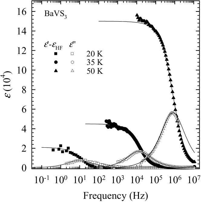
Fig. 1 shows frequency dependence of the complex dielectric response at three selected temperatures. A pronounced dielectric relaxation is observed. The screened loss peak centered at moves toward lower frequencies and smaller amplitudes with decreasing temperature. The main features of this relaxation are well described by the generalized Debye expression , where ( and are static and high-frequency dielectric constant, with the latter being negligible), is the mean relaxation time and is the symmetric broadening of the relaxation time distribution function.
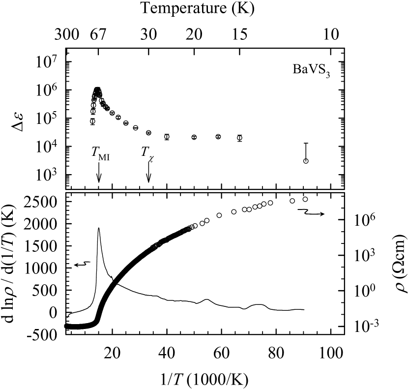
Our results clearly demonstrate that a huge dielectric constant is associated with the metal-to-insulator phase transition (Fig. 2). On decreasing temperature, a sharp growth of starts in the close vicinity of and reaches the huge value of the order of at K (Fig. 2, upper panel). This value corresponds perfectly well to the phase transition temperature as determined in the dc resistivity measurements, indicated by pronounced peaks at in the logarithmic derivative of resistivity (Fig. 2, lower panel).
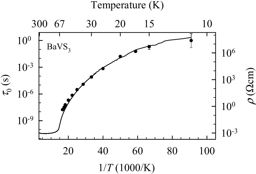
The observed dielectric relaxation would suggest a charge-density wave formation at Gruener88 . The standard model of a deformable CDW pinned in a non-uniform impurity potential accounts for the existence of two modes, transverse and longitudinal Littlewood87 . The former couples to the electromagnetic radiation and yields an unscreened pinned mode in the microwave region. Unfortunately, no microwave measurements on BaVS3 have been done yet. The longitudinal mode couples to an electrostatic potential and mixes in the transverse response due to the non-uniform pinning resulting in an overdamped low-frequency relaxation at due to screening effects. The relaxation detected in our experiments bears two features as expected in the standard model. The first is that the relaxation time distribution is symmetrically broadened, . The second is that the mean relaxation time closely follows a thermally activated behavior similar to the dc resistivity = (see Fig. 3). ns describes the microscopic relaxation time of the collective mode and the gap K, as found in the spectra of the optical conductivity Kezsmarki06 . The dissipation can be naturally attributed to the screening due to single particles originating from the wide band. However, our discovery finds no consistent explanation within the standard model Gruener88 , since the dielectric constant displays a strong decrease below and levels off at temperatures below about 30 K, a behavior which significantly deviates from the one expected for a CDW condensate density : . The decrease of on moving between the MI transition and the magnetic transition is substantial and amounts to two orders of magnitude. One possible explanation for this discrepancy is the very nature of the standard model for the response of the conventional CDW to applied electric fields in which the long-wavelength collective CDW excitation s.c. phason keeps the prominent role. We remind that this model is worked out for the incommensurate CDW in a random impurity potential, whereas the CDW in BaVS3 associated with the observed lattice modulation is commensurate with the order of commensurability, i.e. the ratio of the CDW and lattice periodicity, . However, the order of commensurability is not too high to impose the commensurability pinning and forbid the phason excitations LRA74 . Indeed, the experimental observation of the broad relaxation, i.e. indicates a randomness of the background structure.
Another puzzling feature is brought by the dc electric-field dependent measurements. In the standard 1D CDW compounds, the collective CDW mode couples to an applied dc electric field and gives a novel contribution to the electrical conductivity Gruener88 . Our dc electric-field dependent measurements up to fields as high as 100 V/cm in the temperature range between 15 K and 40 K have only revealed a negligibly small non-linear conductivity, which emerges from the background noise.
III Discussion
Our results indicate that the long-wavelength CDW collective excitations are frozen or strongly renormalized and that the collective excitations of different kind should be responsible for the observed dielectric relaxation. In the following we first address other possible causes and then offer the most plausible scenario for our results.
First, we verify if the observed behavior of the dielectric constant might be due to the hopping conduction which is known to arise in disordered systems with low dimensionality, where Anderson localization yields the conductivity characterized by variable-range hopping (VRH) Mott law in dc limit, while in ac limit it follows a power law dependence on frequency. Although BaVS3 may be regarded as a quasi-1D system, the hopping scenario does not seem realistic for the following reasons. First is that the frequency marking the onset of the frequency-dependent transport is known to be roughly proportional to the dc conductivity, i.e. to the inverse of the dc resistivity Dyre00 . The dc resistivity of BaVS3 at RT is about cm and at lowest temperatures it is about to cm. In the diverse systems with dc resistivities of similar orders of magnitude, the ac conductivity power law is observed only at frequencies above 1 MHz, whereas below 1 MHz an influence of hopping on dielectric dispersion is detected only for dc resistivities much higher than cm.Lunkenheimer03 ; Vuletic03 Indeed, in the case of BaVS3 a crude estimate for the crossover frequency yields values far above the frequency range where the dielectric response was observed Vuletic03 . The second result which excludes hopping comes from the observed optical spectra Kezsmarki06 . Namely, a simple indication for existence of a hopping mechanism would be that the optical conductivity is significantly enhanced in comparison with the dc conductivity, whereas in the case of BaVS3 the optical conductivity, even at temperatures lower than , is at best comparable to the dc conductivity.
Next possible origin of the observed dielectric response might be associated with a ferroelectric nature of the MI transition. Simple space group considerations indicate that below the MI transition the structure of BaVS3 is noncentrosymmetric with a polar axis in the reflection plane containing the VS3 chains. The symmetry of this low-temperature superstructure is Im, implying that the distortions of the two chains of the unit cell are out of phase Fagot05 . Bond-valence sum (BVS) calculations of these X-ray data have indicated some charge disproportionation at low temperatures. However, it was recently argued by P. Foury-Leylekian Foury07 that the BVS method overestimated the charge disproportionation due to several reasons: a nonsymmetric V4+ environment, thermal contraction corrections which were not included and rather imprecise atomic coordinates which were used. Taking all this into account together with X-ray anomalous scattering result that showed negligible redistribution, not larger than 0.01 electron below Fagot06 , we conclude that ferroelectricity cannot provide an explanation of the dielectric response in BaVS3.
Finally, we address orbital ordering as a plausible ground state whose collective excitations might yield the observed dielectric relaxation. First we list arguments developed by Fagot et al. Fagot06 who invoked an orbital ordering associated with the MI phase transition in order to consistently explain structural data of BaVS3. Supporting results for an orbital ordering scenario at are an almost non-existant charge modulation in the insulating phase, together with a qualitative structural analysis of the VS6 octahedron distortions, which reveals an out-of-phase modulation of the occupancy of V sites by the and orbitals. In particular, dominant and occupancies are proposed for V1 and V3 sites respectively, while no definitive preferential occupancy was found for V2 and V4 sites. Furthermore, recent LDA+DMFT (local density approximation with dynamical mean-field theory) calculations performed in the monoclinic insulating phase of BaVS3 have qualitatively confirmed an orbital-ordering scenario showing a V-site-dependent orbital occupancy and only minor, if any, charge disproportionation Lechermann07 . However, these calculations suggest quite different orbital occupancies: it appears that the (V3,V4) pair forms a correlated dimer with mixed and occupancy, while the V1 and V2 ions bear major occupancy and negligible coupling. Finally, the overall study indicates that although the local environment of the V site does not change substantially, the electronic structure turns out to be rather sensitive to change of temperature. The question arises what is the temperature dependence of the order parameter of orbital ordering which starts to develop below and in what way it relates to the magnetic ordering. 51V NMR and NQR measurements also suggested an orbital ordering below that is fully developed only at Nakamura97 . The magnetic phase transition at is preceded by long-range dynamic AF correlations all the way up to and this phase bears features of a gapped spin-liquid-like phase. Mihály et al. Mihaly00 suggested that the lack of magnetic long-range order between and might be the consequence of the frustrated structure of a triangular array of V chains, which also prevents the orbital long-range order, so that the long-range spin and orbital orders can develop only well below . Finally, the AF static order below is not a conventional Néel phase: an AF domain structure is suggested by the magnetic anisotropy measurements Miljak07 . The existence of domains seems to be supported also by the muon spin rotation (SR) measurements, which showed an essentially random distribution of sizeable static electric fields below indicating an incommensurate or disordered magnetism Higemoto02 .
Based on the considerations above we suggest the following as the most plausible scenario. The primary order parameter for the MI phase transition is 1D CDW instability and this CDW instability drives the orbital ordering via structural changes involving a transformation from the orthorhombic to monoclinic with internal distortions of VS6 octahedron and tetramerization of V4+ chains. The orbital order is coupled with the spin degrees of freedom and drives the spin ordering into an AF-like ground state below 30 K. In other words, the orbital ordering transition happens at , domains of orbital order gradually develop in size with lowering temperature (concomitantly their number diminishes) and the long-range order eventually stabilizes below , albeit domain structure persists. In this scenario we propose that the collective excitations responsible for the observed features of the dielectric relaxation are short-wavelength ones, like charge domain walls note in the random AF domain structure. Similar short-wavelength excitations associated with domain structure have previously been invoked as the origin of dielectric relaxation in diverse systems Okamoto91 ; Pinteric99 . The relaxation happens between different metastable states, which correspond to local changes of the spin configuration. The spin configuration is intimately connected with the charge and the orbital degrees of freedom as explained above. Since the dielectric constant is associated with the density of collective excitations, its anomalous temperature behavior below indicates that the relaxation-active number of domain walls decreases with lowering temperature and eventually becomes well defined below . In other words, the dynamics of domain walls becomes progressively more restricted as the temperature lowers and it becomes constant below .
IV Conclusion
In conclusion, we demonstrated the appearance of a huge dielectric constant associated with the metal-to-insulator phase transition in BaVS3 followed by a dramatic decrease on cooling down to the magnetic transition and leveling off below. We argue that the collective excitations whose dispersion we detect as broad screened relaxation modes are not CDW phason excitations; rather they represent short-wavelength excitations of an orbital ordering, which sets in at the metal-to-insulator transition and develops the long-range order below the magnetic transition. Finally, BaVS3 represents a beautiful example of the intricate interplay between an orbital degeneracy on the one side, and spin and charge sector on the other side. This interplay needs to be taken into account in order to understand the origin of the metal-to-insulator phase transition and low-temperature phases in the transition metal compounds in general. Further work on the theoretical and experimental fronts is needed to demonstrate directly the existence of an orbital order in BaVS3 and the associated superstructure.
We thank N. Barišić, S. Barišić, P. Foury-Leylekian, V. Ilakovac, M. Miljak and J. P. Pouget for useful discussions. This work was supported by the Croatian Ministry of Science, Education and Sports under Grant No.035-0000000-2836. The work in Lausanne was sponsored by the Swiss National Science Foundation through the NCCR pool MaNEP.
References
- (1) P. Fulde, Electron Correlations in Molecules and Solids, 3rd edition, Springer-Verlag, Berlin (1995).
- (2) S. Maekawa, T. Tohyama, S. E. Barnes, S. Ishihara, W. Koshibae, and G. Khaliullin, Physics of Transition Metal Oxides, Springer, Berlin (2004).
- (3) D. I. Khomskii, Physica Scripta 72, CC8-14 (2005).
- (4) L. Paolasini, C. Vettier, F. de Bergevin, F. Yakhou, D. Mannix, A. Stunault, W. Neubeck, M. Altarelli, M. Fabrizio, P. A. Metcalf, and J. M. Honig, Phys. Rev. Lett. 82, 4719 (1999).
- (5) H. F. Pen, J. van den Brink, D. I. Khomskii, and G. A. Sawatsky, Phys. Rev. Lett. 78, 1323 (1997).
- (6) M. H. Whangbo, H. J. Koo, D. Dai, and A. Villesuzanne, J. Solid State Chem. 165, 345 (2002) and 175, 384 (2003).
- (7) F. Lechermann, S. Biermann, and A. Georges, Phys. Rev. Lett. 94, 166402 (2005).
- (8) F. Lechermann, A. Georges, A. Poteryaev, S. Biermann, M. Posternak, A. Yamasaki, and O. K. Andersen, Phys. Rev. B 74, 125120 (2006).
- (9) F. Lechermann, S. Biermann, and A. Georges, Phys. Rev. B 76, 085101 (2007).
- (10) S. Fagot, P. Foury-Leylekian, S. Ravy, J. P. Pouget, and H. Berger, Phys. Rev. Lett. 90, 196401 (2003).
- (11) G. Mihály, I. Kézsmárki, F. Zamborszky, M. Miljak, K. Penc, P. Fazekas, H. Berger, and L. Forró, Phys. Rev. B 61, R7831 (2000).
- (12) H. Nakamura, T. Yamasaki, S. Giri, H. Imai, M. Shiga, K. Kojima, M. Nishi, K. Kakurai, and N. Metoki, J. Phys. Soc. Jpn. 69, 2763 (2000).
- (13) S. Fagot, P. Foury-Leylekian, S. Ravy, J. P. Pouget, M. Anne, G. Popov, V. Lobanov, and M. Greenblatt, Solid. State. Sci. 7, 718 (2005).
- (14) S. Fagot, P. Foury-Leylekian, S. Ravy, J. P. Pouget, E. Lorenzo, Y. Joly, M. Greenblatt, M. V. Lobanov, and G. Popov, Phys. Rev. B 73, 033102 (2006).
- (15) M. Pinterić, T. Vuletić, S. Tomić, and J. U. von Schütz Eur. Phys. J. B 22, 335 (2001).
- (16) G. Grüner, Rev. Mod. Phys. 60, 1129 (1988).
- (17) P. B. Littlewood, Phys. Rev. B 36, 3108 (1987).
- (18) I. Kézsmárki, G. Mihály, R. Gaal, N. Barišić, A. Akrap, H. Berger, L. Forró, C. C. Homes, and L. Mihály, Phys. Rev. Lett. 96, 186402 (2006).
- (19) P. A. Lee, T. M. Rice, and P. W. Anderson, Solid. State. Commun. 14, 703 (1974).
- (20) J. C. Dyre and T. B. Schrøder, Rev. Mod. Phys. 72, 873 (2000).
- (21) P. Lunkenheimer, T. Rudolf, J. Hemberger, A. Pimenov, S. Tachos, F. Lichtenberg, and A. Loidl, Phys. Rev. B 68, 245108 (2003).
- (22) T. Vuletic, B. Korin-Hamzic, S. Tomic, B. Gorshunov, P. Haas, M. Dressel, J. Akimitsu, T. Sasaki, and T. Nagata, Phys. Rev. B 67, 184521 (2003).
- (23) P. Foury-Leylekian, Habilitation Thesis, Université Paris-Sud (2007) (unpublished).
- (24) H. Nakamura, H. Imai, and M. Shiga, Phys. Rev. Lett. 79, 3779 (1997).
- (25) M. Miljak (unpublished).
- (26) W. Higemoto, A. Koda, G. Maruta, K. Nishiyama, H. Nakamura, S. Giri, and M. Shiga, J. Phys. Soc. Jpn. 71, 2361 (2002).
- (27) We note that the domain wall and soliton both stand for short wavelength excitations; however whereas soliton is usually a one-dimensional object, the domain wall is not dimensionally restricted.
- (28) H. Okamoto, T. Mitani, Y. Tokura, S. Koshihara, T. Komatsu, Y. Iwasa, T. Koda, and G. Saito, Phys. Rev. B 43, 8224 (1991).
- (29) M. Pinteric, M. Miljak, N. Biskup, O. Milat, I. Aviani, S. Tomic, D. Schweitzer, W. Strunz, and I. Heinen, Eur. Phys. J. B 11, 217 (1999).