Atom Chips
Abstract
Atoms can be trapped and guided using nano-fabricated wires on surfaces, achieving the scales required by quantum information proposals. These Atom Chips form the basis for robust and widespread applications of cold atoms ranging from atom optics to fundamental questions in mesoscopic physics, and possibly quantum information systems.
pacs:
PACS number(s): 03.75.Be, 03.65.NkIn mesoscopic quantum electronics, electrons move inside semiconductor structures and are manipulated using potentials where at least one dimension is comparable to the de-Broglie wavelength of the electrons [1, 2]. Similar potentials can be created for neutral atoms moving microns above surfaces, using nano-fabricated charged and current carrying structures [3, 4, 5]. Surfaces carrying such structures form Atom Chips which, for coherent matter wave optics, may form the basis for a variety of novel applications and research tools, similar to what integrated circuits are for electronics.
In this work we make use of the magnetic interaction based on the coupling of the atomic magnetic moment to the magnetic field to trap and manipulate atoms close to the surface of an Atom Chip. The trapping potentials are created by superposing a homogeneous magnetic bias field with the field generated by a thin current carrying wires. The trap depth is given by the homogeneous field, the gradients and curvatures by the magnetic fields from the wire [4, 6].
We have previously reported on the manipulation of neutral atoms using thin (down to below ) charged wires [7] and current carrying wires (down to ) to form guides [6, 8], beam splitters [4], and Z or U shaped 3-dimensional traps [9]. These structures were free standing.
The next step was to turn to surface mounted wires [10] which was recently achieved for large structures [11, 12]. However,the full potential in surface mounted atom optics lies in the robust miniaturization down to the mesoscopic scale. Such a move is primarily motivated by the theoretically required scale needed to achieving entanglement with neutral atoms through controlled collisions [13] or cavity QED [14], entanglement being the basic building block for quantum information devices.
Here we present such a nanofabricated device with which the required ground state size of less than was achieved. This is a first step towards our vision, the realization of a fully integrated Atom Chip. We start by describing the chip and the experimental setup, followed by a presentation of the results. Finally, we discuss potential applications and future perspectives.
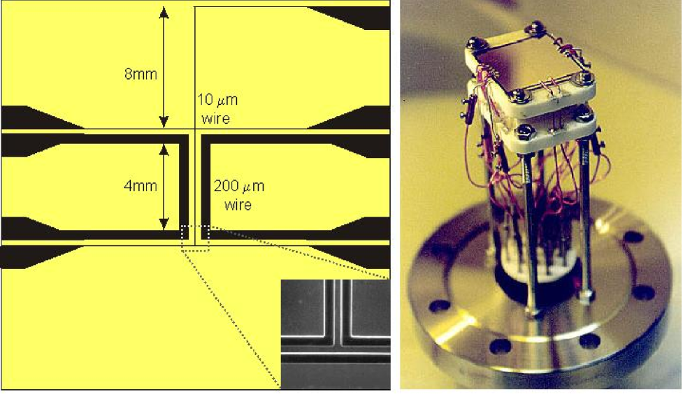
The chip we have used in this work is made of a gold layer placed on a thick GaAs substrate [16]. The gold layer is patterned using nano-fabrication technology. The scale limit of the process used is well below .
In figure 1a we present the main elements of the chip design used in the work described here. Each of the large U-shaped wires, together with a bias field, creates a quadrupole field, which may be used to form a Magneto-Optical-Trap (MOT) on the chip as well as a magnetic trap. Both U-shaped wires together may be used to form a strong magnetic trap in order to ’load’ atoms into the smaller structures, or as an on-board (i.e. without need for external coils) bias field, for guides and traps created by the thin wire running between them. The thin wires are wide and depending on the contact used, may form a U-shaped or a Z-shaped magnetic trap or a magnetic guide. The chip wires are all defined by boundaries of wide etchings in which the conductive gold has been removed. This leaves the chip as a gold mirror (with etchings) and it can be used to reflect the laser beams for the MOT during the cooling and collecting of atoms. Figure 1b presents the mounted chip before it is introduced into the vacuum chamber. In addition, a U-shaped thick wire, capable of carrying up to of current, has been put underneath the chip in order to assist with the loading of the chip. Its location and shape are identical to those of one of the U-shaped wires and it differs only in the amount of current it can carry.
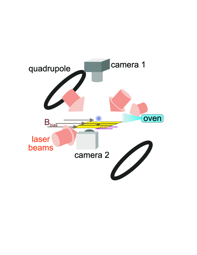
The chip assembly (Fig. 1b) is then mounted inside a vacuum chamber used for atom trapping experiments, with optical access for the laser beams and the observation cameras and with the possibility of applying the desired bias fields (Fig. 2). For a more detailed description of the apparatus and the atom trapping procedure, see [4, 6, 15].
The experimental procedure for loading cold atoms into the small traps on the chip is the following:
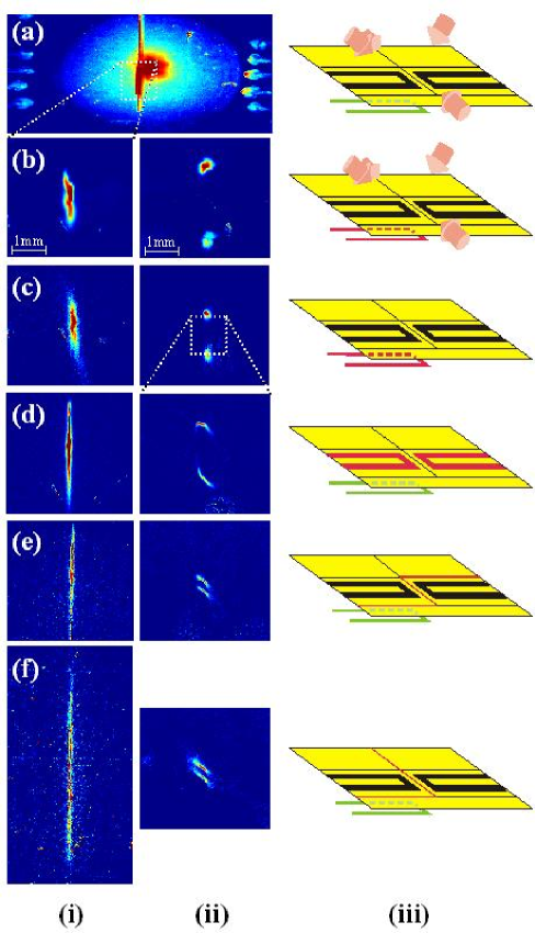
In the first step typically atoms are loaded from an effusive atomic beam into a MOT [17]. Because the atoms have to be collected a few millimeters away from a surface we use a ’reflection’ MOT [18]. Thereby, the 6 laser beams needed for the MOT are formed from 4 beams by reflecting two of them off the chip surface (Fig. 2). Hence atoms above the chip actually encounter six light beams. To assure a correct magnetic field configuration needed for the formation of a MOT, one of the reflected light beams has to be in the axis of the MOT coils. Figure 3a shows a top view of the chip and the reflection MOT sitting above the U-shaped wires.
The large external quadrupole coils are then switched off while the current in the U-shaped wire underneath the chip is switched on (up to ), together with an external bias field (). This forms a nearly identical, but spatially smaller, quadrupole field as compared to the fields of the large coils. The atoms are thus transferred to a secondary MOT which by construction is always well aligned with the chip (Fig. 3b). By changing the bias field, the MOT can be shifted close to the chip surface (typically, ). The laser power and detuning are changed to further cool the atoms, giving us a sample with a temperature below .
In the next step, the laser beams are switched off and the quadrupole field serves as a magnetic trap in which the low field seeking atoms are attracted to the minimum of the field. Without the difficulties of near surface shadows hindering the MOT, the magnetic trap can now be lowered further towards the surface of the chip (Fig. 3c). This is simply done by increasing the bias field (up to ). Atoms are now close enough so that they can be trapped by the chip fields. The loading of the chip has begun.
Next, 2A are sent through each of the two U-shaped wires on the chip and the current in the U-shaped wire located underneath the chip is ramped down to zero. This procedure brings the atoms even closer to the chip, compresses the trap considerably, and transfers the atoms to a magnetic trap formed by the currents in the chip. The distances of the atoms from the surface are now typically a few hundred microns (Fig. 3d).
Finally, the wire trap is loaded in much the same way. It first receives a current of . Then the current in both the U-shaped wires is ramped down to zero (Fig. 4). Atoms are now typically a few tens of microns above the surface (Fig. 3e).
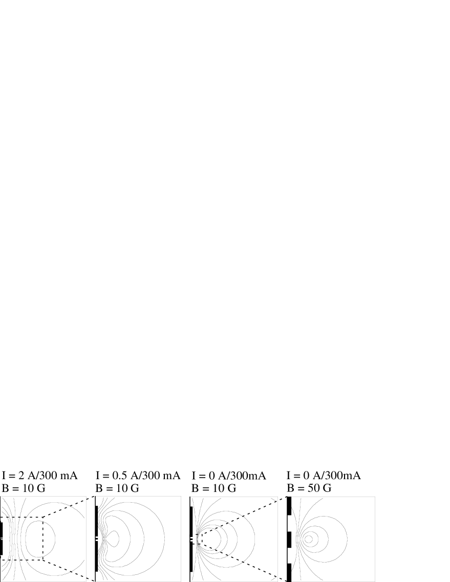
These guides and traps can be further compressed by ramping up the bias magnetic field. In this process we typically achieve gradients of . By applying a bias field of and a current of in the wire we achieve trap parameters with a transverse ground state size below 100 nm and frequencies of above (as required by the quantum computation proposals [13]).
By running the current through a longer section of the thin wire, we turn the magnetic trap into a guide, and atoms could be observed expanding along it (Fig. 3f).
In an additional experiment we used the thick wires on the chip to create an on chip bias fields for the trapping. In the experiment this is done by sending current through the two U-traps in the opposite direction with respect to the current in the wire, which creates a magnetic field parallel to the chip surface. Hence, we demonstrate trapping of atoms on a self contained chip.
In these small traps, the atom gas can be compressed to the point where direct visual observation is difficult. In such a case, we observe those atoms after guiding or trapping, by ’pulling’ them up from the surface into a less compressed wire trap (by increasing the wire current or decreasing the bias field).
During the transfer from the large magnetic trap to the small 10 trap the density of the atomic cloud is increased by up to a factor 350. As the trap is compressed, the temperature of the atoms rises, and if in this course the trapping potential is not deep enough atoms are lost. In our case, the trap depth is uniquely determined by the bias field used, which leads to depths ranging between () for the bias field and to () for the bias field and . This adiabatic heating and the finite trap depth limited the transfer efficiency for atoms from the large magnetic quadrupole into the smallest chip trap to 50 %.
Since we use an trapped atomic sample consisting of 3 different spin states (, , and ) the large compression also increases the rate for inelastic two body spin flip collisions dramatically. This rate is for our Li sample similar to the elastic collision rate [19] and is therefore a good estimate of the achievable collision rates in a polarized sample. From measured decay curves we estimate the collision rate to be in the order of 20 for atoms in a typical small chip trap. This estimate of the scattering rate in the small chip traps is supported by the observation that the atoms expand very fast into the wire guide, indicating that energy gained from the transverse compression of the trap is transformed efficiently into longitudinal velocity at a very high rate.
The above shows that the concept of an Atom Chip clearly works. We have demonstrated that a wide variety of magnetic potentials may be realized with simple wires on surfaces. Wires together with a bias field can produce quadrupole fields for a MOT, 3D minima for trapping, and 2D minima for guiding. Furthermore it is very easy to manipulate the center of the trap and its width. We have shown that loading such an atom trap above the surface does not present a major problem and trap parameters with a transverse ground state size below and frequencies of above have been achieved. In addition we could trap atoms exclusively with the chip fields, creating the required bias fields ’on board’. Last but not least, it has been shown that standard nano-fabrication techniques and materials may be utilized to build these Atom Chips. The wires on the surface can stand sufficiently high current densities () in vacuum and at room temperature. Together with the scaling laws of these traps [4, 6, 9], this will allow us to use much thinner wires and reach traps with ground state sizes of and trap frequencies in the MHz range.
We conclude with a long term outlook. In this work we have successfully realized a step which is but one of many still needed. A final integrated Atom Chip, should have a reliable source of cold atoms, for example a BEC [20], with an efficient loading mechanism, single mode guides for coherent transportation of atoms, nano-scale traps, movable potentials allowing controlled collisions for the creation of entanglement between atoms, extremely high resolution light fields for the manipulation of individual atoms, and internal state sensitive detection to read out the result of the processes that have occurred (e.g. the quantum computation). All of these, including the bias fields and probably even the light sources, could be on-board a self-contained chip. This would involve sophisticated 3D nano-fabrication and the integration of a diversity of electronic and optical elements, as well as extensive research into fundamental issues such as decoherence near a surface. Such a robust and easy to use device, would make possible advances in many different fields of quantum optics: from applications in atom optics [21] such as clocks and sensors to implementations of quantum information processing and communication [22].
We would like to thank A. Chenet, A. Kasper and A. Mitterer for help in the experiments. Atom chips used in the preparation of this work and in the actual experiments were fabricated at the Institut für Festkörperelektronik, Technische Universität Wien, Austria, and the Sub-micron center, Weizmann Inst. of Science, Israel. We thank E.Gornik, C. Unterrainer and I. Bar-Joseph of these institutions for their assistance. Last but not least, we gratefully acknowledge P. Zoller and T. Calarco who are responsible for the theoretical vision. This work was supported by the Austrian Science Foundation (FWF), project S065-05 and SFB F15-07, the Jubiläums Fonds der Österreichischen Nationalbank, project 6400, and by the European Union, contract Nr. TMRX-CT96-0002. B.H. acknowledge financial support form Svenska Institutet.
REFERENCES
- [1] Y. Imry, Introduction to Mesoscopic Physics, Oxford University Press, Oxford 1987.
- [2] E. Buks, R. Schuster, M. Heilblum, D. Mahalu, V. Umansky, Nature 391, 871-874 (1998).
- [3] J. Schmiedmayer, Eur. Phs. J. D 4, 57 (1998).
- [4] J. Denschlag, D. Cassettari, A. Chenet, S.Schneider, J. Schmiedmayer, Appl. Phys. B 69, 291 (1999).
- [5] E.A. Hinds, I.G. Hughes, J. Phys. D 32, R119 (1999).
- [6] J. Denschlag, D. Cassettari, J. Schmiedmayer, Phys. Rev. Lett. 82, 2014 (1999).
- [7] J. Denschlag, G. Umshaus, J. Schmiedmayer, Phys. Rev. Lett. 81, 737 (1998).
- [8] J. Schmiedmayer in XVIII International Conference on Quantum Electronics: Technical Digest, edited by G. Magerl (Technische Universität Wien, Vienna 1992), Series 1992, Vol. 9, 284 (1992); Appl. Phys. B 60, 169 (1995); Phys. Rev. A 52, R13 (1995).
- [9] A. Haase, D. Cassettari, B. Hessmo, J. Schmiedmayer, Submitted to Phys. Rev. A.
- [10] J.D. Weinstein, K. Libbrecht, Phys. Rev. A 52, 4004 (1995); M. Drndic et al., Appl. Phys. Lett. 72, 2906 (1998);
- [11] Fortagh et al. Phys. Rev. Lett. 81, 5310 (1998);
- [12] J. Reichel, W. Hänsel, T.W. Hänsch, Phys. Rev. Lett. 83, 3398 (1999); D. Müller et al., Pre-print Physics/9908031; N. H. Dekker, et al., Los Alamos e-print archive: physics/9908029;
- [13] D. Jaksch et al., Phys. Rev. Lett 81, 3108 (1998); D. Jaksch et al., Phys. Rev. Lett 82, 1975 (1999); H.J.Briegel et al., J. Mod. Optics, (in print 1999); T.Calarco et al., Phys. Rev. A (in print 1999), (quant-ph/9905013).
- [14] S. J. Van Enk, J. I. Cirac, P. Zoller, Science 279, 205 (1998)
- [15] J. Denschlag, PhD Thesis, Universität Innsbruck (1998).
- [16] The chip is produced using standard nano-fabrication methods. A detaíled account will be given in: T. Maier et al., to be published.
- [17] The atoms are loaded into the MOT for out of an effusive beam at a red laser detuning of and a total laser power of about . An electro-optic modulator produces sidebands of one of which is used as a repumper. To increase the loading rate we use an additional slower beam (, red detuned) directed through the MOT into the oven. The MOT is typically in diameter (FWHM) and has a temperature of T 200 K which corresponds to a velocity of about .
- [18] K.I. Lee, J.A. Kim, H.R. Noh, W. Jhe, Opt. Lett. 21, 1177 (1996).
- [19] Robin Côté, private communication.
- [20] M. H. Anderson et al., Science 269, 198 (1995); K. B. Davis et al., Phys. Rev. Lett. 75, 3969 (1995); C. C. Bradley et al., Phys. Rev. Lett. 75, 1687 (1995); For an extensive list of references see: http://amo.phy.gasou.edu/bec.html/bibliography.html
- [21] For an overview see: C.S. Adams, M. Sigel, J. Mlynek, Phys. Rep. 240, 143 (1994); Atom Interferometry, edited by P. Berman (Academic Press, 1997).
- [22] The Physics of Quantum Information edited by, D. Bouwmeester, A. Ekert, and A. Zeilinger, Springer-Verlag 2000.