]School of Electronics and Computer Science, Southampton University, UK. ]Centre for Cold Matter, Blackettt Laboratory, Imperial College London, UK ]School of Electronics and Computer Science, Southampton University, UK. ]Centre for Cold Matter, Blackettt Laboratory, Imperial College London, UK
The effect of self-affine fractal roughness of wires on atom chips
Abstract
Atom chips use current flowing in lithographically patterned wires to produce microscopic magnetic traps for atoms. The density distribution of a trapped cold atom cloud reveals disorder in the trapping potential, which results from meandering current flow in the wire. Roughness in the edges of the wire is usually the main cause of this behaviour. Here, we point out that the edges of microfabricated wires normally exhibit self-affine roughness. We investigate the consequences of this for disorder in atom traps. In particular, we consider how closely the trap can approach the wire when there is a maximum allowable strength of the disorder. We comment on the role of roughness in future atom–surface interaction experiments.
I Introduction
Atom chips are microfabricated structures that allow the preparation and manipulation of cold atom clouds or Bose–Einstein condensates (BEC) above a substrate surface. Often, these structures use current-carrying wires to produce tightly confining magnetic microtraps close to the substrate surface, where atom clouds can be held still, transported, or split Hinds2001 ; Fortagh98 ; Denschlag99 ; Key2000 ; Fortagh07 . With the integration of optical components Eriksson05 and movable structures Gollasch05 into atom chips, new possibilities are now opening for neutral atoms on a chip to form quantum sensors, clocks and information processors Calarco04 . However, the homogeneity and stability of atom clouds can be compromised close to a metallic surface by physical factors that cause fragmentation and/or the loss of atoms. Two main phenomena have been identified: (i) spatial imperfections of the wire, which cause the current to flow non-uniformly and make the atom trap rough, and (ii) thermal fluctuations of the magnetic field near the surface, which drive spin flips of the atoms and cause loss Jones03 . The first of these is the subject of our paper.
Recently, the corrugation of magnetic fields close to a wire has been studied extensively. Initial experiments showed that atom clouds break up into fragments as they approach the surface Zimmermann1 ; Jones04 , then it was demonstrated that this is due to a magnetic field component parallel to the wire Zimmermann2 , caused by transverse components of the current density. Some theoretical efforts were made to relate this to the details of the current flow Jones04 and to roughness of the surface and irregularity in the edges of the wire Wang04 ; Schumm05 , which cause the current to meander. If the meander has a single spatial Fourier component of wavevector , the decay of this anomalous field decreases with distance above the wire according to the Bessel function to a good approximation Jones04 . When the transverse current has a broad noise spectrum, this decay can sometimes be described by a power law Zimmermann2 .
Conductors lithographically patterned on an atom chip are usually fabricated with good bulk homogeneity in order to minimise this potential problem of magnetic roughness. The width of the wire is typically comparable to the distance between the magnetic trap and the surface. In these typical cases, the meandering of the current is driven mainly by the roughness of the edges, as determined by the fabrication process. Three processes are available, namely, (i) electrodeposition of the metal into a mould formed by a thick photoresist Kraft04 ; Schumm05 , (ii) etching of a complete metallic film to create the space between wires Kraft04 using wet chemicals or ion beam milling Lewis06 , and (iii) evaporation of the metal onto the substrate through a mask formed by a patterned resist (the method known as lift-off).
With all these methods of microfabrication, the edges of the wires exhibit self-affine fractal roughness Meakin ; Barabasi , a type of roughness that we now discuss. Consider an edge along the direction with roughness fluctuations . By definition the height-height correlation function is given by , the autocorrelation function is , and the mean square roughness is . The angle brackets denote averaging over the (large) length of the wire. These quantities are connected by the relation . A self-affine fractal edge is one that satisfies the scaling law , where is known as the roughness exponent or Hurst exponent. The statistical properties of such an edge are invariant when the length is scaled by a factor , provided there is an accompanying scaling of the transverse dimension by . Microfabricated edges exhibit precisely this type of behaviour on small length scales Constantoudis03 up to a characteristic length , known as the correlation length. For , tends to the constant value and the autocorrelation function tends to zero. This behaviour is captured by the empirical autocorrelation function
| (1) |
which has the required assymptotic behaviour at large and small and fits experimental data well Palasantzas93 . The Hurst exponent is normally between 0 and 1 note1 , while the correlation length and rms roughness are both typically in the range 1–100 nm Schumm05 ; Constantoudis03 ; Palasantzas93 .
Considerable progress has been made in understanding how roughness in the edges of a wire can generate roughness in the magnetic traps produced by the wire Jones04 ; Wang04 ; Schumm05 . However, the analyses to date have considered edges with a white noise spectrum or other rather specific model spectra. Here we reconsider the magnetic noise of atom traps, taking into account this realistic and more generally applicable model of the self-affine fractal edge roughness.
II Description of self-affine roughness along an edge
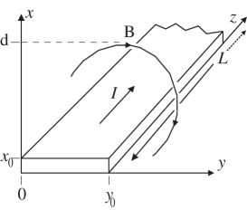
Figure 1 defines a coordinate system and shows the wire that we are considering. The left and right edges of the wire lie on and with fluctuations and respectively. Hence the centre of the wire lies on , where , with correlation function . We take as our starting point the empirical correlation function given in equation (1). In the particular case when , the corresponding power spectrum has the Lorentzian form
| (2) |
where spans the range to . In order to have analytical results for a more general range of possibilities, we extend the power spectrum of equation (2) to the form
| (3) |
This is a one-dimensional version of the approximation introduced by Palasantzas (section IV of Palasantzas93 ) to describe surface noise. The parameter in the denominator of this spectrum is needed to ensure that the integral of equation (3) over all yields the mean square roughness . This normalisation condition requires
| (4) |
where is the Euler function. We find by direct numerical integration that the power spectrum corresponding to equation (1) is reasonably well reproduced by equation (3), but only over the range . Figure 2 shows the dimensionless spectrum , defined in equation (3), for these two extremes of the Hurst exponent . At low frequency it has the value regardless of , but as the frequency increases, the spectrum with lower also has lower noise. At higher frequency still, this necessarily reverses because these spectra are normalised. Typical profiles of the centre position , plotted over a length , are inset into the figure to illustrate this. The case of exhibits more high-frequency noise but less long-wavelength noise than that of .
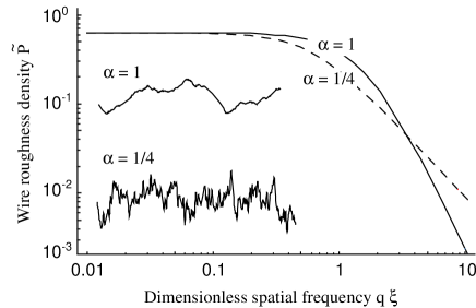
This model is expected to describe fluctuations in the centre of a wire fabricated on an atom chip. In particular, it describes the atom chip wires currently being used at Imperial College London, which are made by ion beam milling a gold film. These typically have roughness nm, correlation length nm and Hurst exponent . The noise reported in figure 8 of Schumm et al. Schumm05 is also consistent with this model, giving for their evaporated wire the values nm, and nm. (Note, however that such analysis of the power spectrum is not a very reliable way to measure or Constantoudis04 ). In the following, we discuss the roughness of the magnetic atom traps produced when current flows through such a wire and we investigate how the field fluctuations vary with the Hurst exponent and correlation length . Wires made by electrodeposition into a thick photoresist mould have so far been much rougher. For example, the electroplated wire of Schumm05 had nm, and nm. Moreover, the spectrum of that wire exhibited a second power-law region with exponent at wavelengths longer than m, indicating a second regime of correlated roughness.
III Roughness of the atom trap formed by a wire
Consider the wire in figure 1. If the current flows uniformly along the -direction, the magnetic field lines lie in the plane. In particular, the field points in the -direction above the centre of the wire. This field is cancelled at a height by applying an opposite uniform bias field and the resulting line of zero magnetic field is surrounded by a transverse quadrupole field. Magnetic atoms can then be trapped at height above the centre of the wire by the magnetic dipole interaction . A small uniform bias field is often applied along the -direction as well, so that the magnetic field minimum goes to rather than to zero. This suppresses the loss of atoms through non-adiabatic spin flips.
In reality, the noise in the edges of the wire causes the current to deviate from side to side, generating a noise field component along the direction. Consequently, the potential energy along the centreline of the trap is no longer the constant but is modulated by noise . Assuming that the wire is thin (along x) compared with the height , the power spectrum of this noise can be written as
| (5) |
where is characteristic of the ideal field produced by the wire and is the power spectrum describing fluctuations in the centre of the wire, which we take here to be given by equation (3). The dimensionless scaling factor translates the noise in the centre of the wire to the noise in the field. It is given by Wang04
| (6) | |||||
where is the modified Bessel function of the second kind and is the incomplete Gamma function. This expansion is useful in the range , where a small number of terms is sufficient to achieve convergence: 50 terms at and fewer terms at larger distance. When , the individual terms become excessively large and the series appears not to converge. In summary, the spectrum of the noise in the magnetic atom trap depends on the Hurst exponent and four length scales: and in , which characterise the roughness of the edges and and in , which define the geometry of the trap. The over-all energy scale is given by .
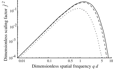
The frequency dependence of is illustrated in figure 3. The three curves correspond to wire widths of (solid line), (dashed) and (dotted). When is small compared with , is quite insensitive to its value, but becomes small for a wider wire as the edges move further away compared with . At low frequencies, i.e. when , the function increases in proportion to , reaching a maximum in the vicinity of . For large , the function decays as . If the current wanders periodically from side to side with a given amplitude, the angular variation of the current density is inversely proportional to the wavelength. Consequently, the transverse component is proportional to the frequency . This is the physical cause of the linear cutoff in at low-frequency. The exponential (Bessel) cutoff at high frequency is due to Laplace’s equation for the magnetostatic potential, which naturally smoothes high frequency ripples as one goes far away from the wire.
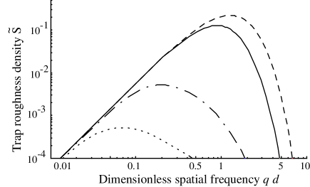
The dimensionless spectrum of the noise in the trapping potential (see equation (5)) is the product of the two spectra and , shown in figures 2 and 3. Whereas depends on the frequency through , is a function of , therefore the shape of the spectrum depends on the ratio as illustrated in figure 4. The dashed curve in figure 4 represents the case of short correlation length, , for which over the whole range of the graph, making constant at . In this limit, equation (5) gives , a spectrum that is independent of the wire roughness except for the in the over-all scale factor. This general behaviour of a spectrum proportional to persists throughout the range , as also indicated by the solid line representing . At the other extreme, the dotted curve in figure 4 represents the case of long correlation length, , for which over the whole range of interest, giving and therefore . This general behaviour of is characteristic of the whole range , as also illustrated by the dash-dotted line in figure 4.
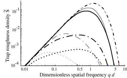
Figure 5 shows the effect of changing the Hurst exponent in the roughness spectrum of the wire from , as in figure 4 (light curves), to (heavy curves). When (dashed curves), the change of Hurst exponent makes no difference because the spectrum is essentially independent of . By contrast, the dotted curves representing exhibit a strong dependence on the Hurst exponent. Reducing from 1 to 1/4 suppresses the low frequency noise and increases the power at higher frequencies, as already noted in the context of figure 2. This has the effect of moving the peak of the noise spectrum to higher frequencies. The same effect is seen in the dash-dotted curves of figure 5 representing . When is equal to (solid curves), the change to suppresses the low frequency part of the spectrum, but the corresponding increase at higher frequency is not evident because the spectrum is cut off at higher frequencies by the exponential roll-off of the function .
The mean square roughness of , let us call it for variance, is obtained by integrating equation (5) over frequency:
| (7) |
Once again, it is useful to adopt a dimensionless version in order to understand how depends on the various length scales involved. The form
| (8) |
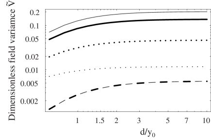
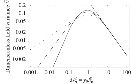
renders the field variance dimensionless and makes it a function of , and . This is plotted versus in figure 6 for three values of and two values of . We see immediately that the dimensionless variance is approximately constant with distance, corresponding to a variation in that weakens when . This result is consistent with experimental observations that the noise decreases with increasing distance from the wire Jones04 ; Zimmermann2 ; Schumm05 . All the dependence on and is contained in , which is largest when (solid lines). Changing from (light curves) to (heavy curves) makes essentially no difference when is small (dashed lines), because is effectively a constant under these conditions, as discussed above. By contrast, the same change of reduces the noise when (solid line) and increases it when (dotted line). Another view of the same parameter space is given in figure 7, which plots the field noise at height versus , for three values of . This shows more clearly the peaking of the noise near , and the insensitivity to the value of the Hurst exponent when is small.
The best present methods for fabricating atom chip wires yield correlation lengths of order 1–100 nm, while current experiments operate at distances in the range 1–100 m. This places experiments firmly in the domain of small , where the value of the Hurst exponent does not influence the roughness of the magnetic trap significantly and we can take . In this regime we find that . For any particular value of we can integrate equation (8) numerically to obtain the constant of proportionality. For example, with we find
| (9) |
For narrower wires, i.e. for , this constant changes very little as we have already seen in figure 6.
IV Consequences for the design of the atom trap
One of the primary motivations for atom chips is to achieve small traps with high trapping frequencies. This requires a high field gradient, which is approximately for narrow wires (by which we mean ). The tightest confinement is achieved by bringing the atoms close to narrow wires, even though smaller wires carry less current Schumm05 , but this also increases the roughness of the magnetic field. In many experiments, the field has a maximum permissible variance, let us call it . For example, a Bose–Einstein condensate will break into separate clouds unless the noise in the trapping potential is smaller than the chemical potential. In these cases, the limit on trap roughness imposes a minimum distance from the surface and hence a maximum achievable magnetic field gradient.
The heat generated by electrical resistance limits the current that can be tolerated in a lithographically fabricated wire to Groth04 , where is the thickness of the wire (figure 1) and the constant characterises the heat flow across the interface between the wire and the substrate. When the maximum current is passed through a wire having , equations (8) and (9) give the variance of as
| (10) |
Upon setting this equal to , we find that the distance of closest approach and the maximum field gradient are
| (11) | |||||
| (12) |
Let us take mG, for which the rms roughness in the potential corresponds to a temperature of 67 nK. We take A m-3/2 Groth04 ; Schumm05 , which is typical for gold wires on a substrate. We further assume the values m, nm, and nm, which are typical of our present wires, as discussed in section II. Then the minimum distance of approach to the wire is m, the current in the wire is mA, and the corresponding maximum field gradient is T cm-1.
In the presence of a bias field along the -direction (figure 1), the potential energy of the trapped atom near its equilibrium position is , where is the transverse () displacement. The corresponding frequency for transverse harmonic oscillations is
| (13) |
where is the mass of the atom. Taking a typical value of G, the maximum transverse frequency for 87Rb atoms in the , ground state is kHz. This result indicates that atom chips can achieve very high trapping frequencies, comparable with those already demonstrated in optical lattices, while remaining adequately smooth. The correspondingly small extension of the vibrational ground state wavepacket is only, 17 nm, making such traps very promising for studing the physics of 1-dimensional cold gases Pricoupenko04 .
V Discussion
We have examined how a magnetic trap formed by a current-carrying wire is sensitive to the roughness on the edges of the wire. In particular, we have extended previous discussions to consider the case of a self-affine fractal roughness spectrum with a correlation length . This is of interest because the methods used to fabricate wires on an atom chip generally produce such roughness. Our analysis has shown how the spectrum of trap roughness involves an interplay between the spectrum of the wire roughness and the spectrum of the transfer function that converts deviations of the current into fluctuations of the magnetic field. In most current experiments, there is a clear hierarchy of length scales in which . When there is also a maximum acceptable roughness of the magnetic trap, this leads to equation (11) for the minimum operating distance between the trap and the wire. There is correspondingly a maximum achievable field gradient given by equation (12). These results argue for minimising the quantity because this determines the spectral density of the edge roughness at low frequency, which is what generates the noise in the magnetic trap. In these cases where , the Hurst exponent is less important because it only affects the spectrum at frequencies above , which do not contribute significantly to the trap roughness. Naturally, if there is a second power-law regime at long wavelength, as in some wires Schumm05 , then the corresponding Hurst exponent significantly affects the magnetic trap roughness at that length scale.
There is considerable interest in trapping atoms much closer to the surface. Atoms trapped at sub-micron distances would begin to probe the details of the short-scale noise and in that case the value of would be significant. In the range of 0.1–1 m one could intentionally create surfaces with a variety of noise spectra in order to propagate BEC through custom-made disorder potentials as a study of quantum localisation phenomena, as proposed by Wang04 . Experiments of this type have already been done using random optical potentials Lye05 ; Schulte05 ; Clement05 , but this magnetic disorder offers a different noise spectrum with the possibility of very short correlation length. The effective amplitude of the noise can be conveniently controlled by appropriate modulations of the currents that form the trap, as recently demonstrated by Trebbia2007 . A natural lower limit to the distance of closest approach is set by the electromagnetic attraction of the atom towards the surface — the Van der Waals (Casimir-Polder) force — which grows as () and overwhelms the trapping force at a distance of order 100 nm Hinds91 ; Hinds94 . This force itself is also of fundamental interest and can be measured further away from the surface by means of cold atoms Hinds94 ; Obrecht07 . Even more exotically, one can hope to measure the gravitational attraction at short range, which might exhibit departures from the Newtonian law as a result of extra dimensions Dimopoulos03 . These experiments also require careful control over the noise of the surface. We note that if the distance to the surface becomes much less than the width of the wire, the corrugation of the surface Schumm05 and imperfections of the bulk Kruger2005 may contribute significantly to the magnetic trap roughness.
In this study we have not considered the role of additional technical noise at long correlation lengths, but such noise certainly exists as a result of imperfections in the fabrication process and can make a significant contribution to the roughness of the magnetic trap at long wavelength. For example, a supposedly straight line may be bent by optical aberrations during the lithographic patterning. A bend of only rad amounts to a deviation of only 10 nm over a length of m. Nevertheless, in a bias field of G this would generate an appreciable unwanted of 1 mG. There can also be a periodic wobble of straight lines due to the imperfection of mechanical translation stages. These kinds of defects are very hard to measure by standard microscopy because they involve small transverse displacements over length scales larger than the normal field of view in an SEM or AFM microscope. In fact, this noise is best measured by the cold atoms themselves through its effect on their density distribution in the trap. Ref. Kruger2005 has already noted that on certain length scales, this method may provide a uniquely sensitive way to probe the magnetic field near surfaces.
Acknowledgements.
This work was supported by the European Commission through the Atom Chips, Conquest and SCALA networks and by the UK through EPSRC and Royal Society funding. We acknowledge valuable discussions with S. Eriksson.References
- (1) E. A. Hinds, C. J. Vale, and M. G. Boshier, Phys. Rev. Lett. 86 1462 (2001).
- (2) J. Fortágh, A. Grossmann and C. Zimmermann, Phys. Rev. Lett. 81 5310 (1998).
- (3) J. Denschlag, D. Cassettari and J. Schmiedmayer, Phys. Rev. Lett. 82 2014 (1999).
- (4) M. Key, I. G. Hughes, W. Rooijakkers, B. E. Sauer, E. A. Hinds, D. J. Richardson and P. G. Kazansky, Phys. Rev. Lett. 84 1371 (2000).
- (5) J. Fortágh and C. Zimmermann, Rev. Mod. Phys. 79 235 (2007).
- (6) S. Eriksson, M. Trupke, H. F. Powell, D. Sahagun, C. D. J. Sinclair, E. A. Curtis, B. E. Sauer, E. A. Hinds, Z. Moktadir, C. O. Gollasch, M. Kraft, Eur. Phys. J. D 35 135 (2005).
- (7) C. O. Gollasch, Z. Moktadir, M. Kraft, M. Trupke, S. Eriksson and E. A. Hinds, J. Micro. Mech. and Micro. Eng. 15 S39 (2005).
- (8) C. Henkel, J. Schmiedmayer, and C. Westbrook, Euro. Phys. J. D 35 1 (2006) and following articles.
- (9) M. P. A. Jones, C. J. Vale, D. Sahagun, B. V. Hall and E. A. Hinds, Phys. Rev. Lett. 91 080401 (2003).
- (10) J. Fortágh, H. Ott, S. Kraft, A. Günther and C. Zimmermann, Phys. Rev. A 66 041604 (2002).
- (11) M. P. A. Jones, C. J. Vale, D. Sahagun, B. V. Hall, C. C. Eberlein, B. E. Sauer, K. Furusawa, D. Richardson and E. A. Hinds , J. Phys. B 37 L15 (2004).
- (12) S. Kraft, A. Günther, H. Ott, D. Wharam, C. Zimmermann and J. Fortágh, J. Phys. B 35 L469 (2002).
- (13) T. Schumm, J. Esteve, C. Figl, J.-B. Trebbia, C. Aussibal, H. Nguyen, D. Mailly, I. Bouchoule, C.I. Westbrook and A. Aspect, Eur. Phys. J. D 32 171 (2005).
- (14) D. W. Wang, M. D. Lukin and E. Demler, Phys. Rev. Lett. 92 076802 (2004).
- (15) E. Koukharenko, Z. Moktadir, M. Kraft, M. E. Abdelsalam, D. M. Bagnall, C. Vale, M. P. A. Jones and E. A. Hinds, Sensors and Actuators A 115 600 (2004).
- (16) G. Lewis, Z. Moktadir, C. O. Gollasch, Kraft, M. Trupke, S. Erikisson and E. A. Hinds, Proceedings of 16th MicroMechanics Europe Workshop (2006).
- (17) P. Meakin, Fractals, scaling and growth far from equilibrium (Cambridge University Press, 1998).
- (18) A. L. Barabasi and H. E. Stanly, Fractal concept in surface growth (Cambridge University Press, 1995).
- (19) V. Constantoudis, G. P. Patsis, A. Tserepi and E. Gogolides, J. Vac. Sci. Tech. B21 1019 (2003).
- (20) G. Palasantzas, Phys. Rev. B 48 14472 (1993).
- (21) When , the surface is said to be super rough. Films grown by molecular beam epitaxy, where surface diffusion is the dominant process, are one example.
- (22) V. Constantoudis, G. P. Patsis, L. H. A. Leunissen and E. Gogolides, J. Vac. Sci. Tech. B 22 1974 (2004).
- (23) S. Groth, P. Krüger, S. Wildermuth, R. Folman, T. Fernholz, J. Schmiedmayer, D. Mahalu and I. Bar-Joseph, Appl. Phys. Lett. 85 2980 (2004).
- (24) Quantum gases in low dimensions, edited by L. Pricoupenko, H. Perrin, and M. Olshanii, special issue of J. Phys. IV 116 1 (2004).
- (25) J. E. Lye, L. Fallani, M. Modugno, D. S. Wiersma, C. Fort, and M. Inguscio, Phys. Rev. Lett. 95 070401 (2005).
- (26) T. Schulte, S. Drenkelforth, J. Kruse, W. Ertmer, J. Arlt, K. Sacha, J. Zakrzewski, and M. Lewenstein, Phys. Rev. Lett. 95 170411 (2005).
- (27) D. Clément, A. F. Varón, M. Hugbart, J. A. Retter, P. Bouyer, L. Sanchez-Palencia, D. M. Gangardt, G.V. Shlyapnikov, and A. Aspect, Phys. Rev. Lett. 95 170409 (2005).
- (28) J.-B. Trebbia, C.L. Garrido Alzar, R. Cornelussen, C.I. Westbrook and I. Bouchoule, arXiv:quant-ph/0701207 (2006).
- (29) E. A. Hinds and V. Sandoghdar, Phys. Rev. A 43 398 (1991).
- (30) E. A. Hinds, Adv. At. Mol. Opt. Phys., Supplement 2, edited by Paul R. Berman (Academic Press, Inc., 1994), p. 1.
- (31) J.M. Obrecht, R.J. Wild, M. Antezza, L. P. Pitaevskii, S. Stringari, and E. A. Cornell, Phys. Rev. Lett. 99 063201 (2007).
- (32) S. Dimopoulos and A. A. Geraci, Phys. Rev. D 68 124021 (2003).
- (33) P. Krüger, S. Wildermuth, S. Hofferberth, L. M. Andersson, S. Groth, I. Bar-Joseph and J. Schmiedmayer, J. of Phys.: Conf. Series 19 56 (2005).