Optical Nanofibers for Manipulating and Probing Single-Atom Fluorescence
Abstract
We demonstrate how optical nanofibers can be used to manipulate and probe single-atom fluorescence. We show that fluorescence photons from a very small number of atoms, average atom number of less than 0.1, around the nanofiber can readily be observed through single-mode optical fiber under resonant laser irradiation. We show also that optical nanofibers enable us to probe the van der Waals interaction between atoms and surface with high precision by observing the fluorescence excitation spectrum.
pacs:
42.50.-p,42.62.Fi,32.80.Qk,39.90.+dRecently, thin optical fibers with subwavelength diameters, termed as optical nanofibers, have attracted considerable attentions. Although thin optical fibers with diameters larger than wavelengths have been used widely for various optical technologies, optical nanofibers are opening many new directions in the field of optical physics. Tong et al. developed a method to fabricate optical nanofibers with diameters down to 50 nm and demonstrated possible wide range of photonic applications like low loss optical waveguiding Mazur . Leon-Saval et al. demonstrated supercontinuum generation using a unique property of propagating field confinement of nanofibers Russell . Sumetsky et al. demonstrated a new type of optical resonator, micro-ring resonator, using evanescent coupling between nanofiber coils Sumetsky .
From a viewpoint of quantum optics, optical nanofiber may become a fascinating work bench due to the possibility of the quantum electrodynamic effects associated with the confinement of the fields in the guided modes. It has been demonstrated theoretically that spontaneous emission of atoms may be strongly enhanced around nanofibers and an appreciable amount of fluorescence photons may be emitted into a single guided mode of the nanofibers SpCont . Furthermore, two distant atoms on the nanofiber surface may be entangled through the guided mode Entangle . Novel atom trapping schemes are also proposed using optical nanofibers Trapping . These possibilities may open new approaches for manipulating single atoms and single photons, which offer new tools for quantum information technology.
In this Letter, we experimentally demonstrate how optical nanofibers can work for manipulating and probing single-atom fluorescence. We use laser-cooled Cs-atoms to realize interaction time longer than the atomic spontaneous emission lifetime. We show that fluorescence photons from atoms around the nanofiber are measured efficiently by observing photons through the fiber guided mode. We show also that due to the inherent nature of the nanofiber method the fluorescence excitation spectrum strongly reflects the effect of van der Waals interaction between atoms and nanofiber surface.
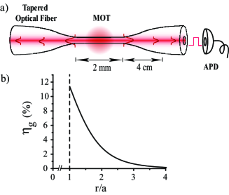
Figure 1(a) shows the diagram of the present experiment. The nanofiber locates at the mid of tapered optical fiber. A key point is the adiabatic tapering of a single mode optical fiber so that the single-mode propagation condition can be maintained for whole fiber length Sumetsky2 . Fluorescence photons emitted into the guided mode are measured through the optical fiber. In Fig. 1(b) is shown the coupling efficiency of spontaneous emission into each direction of the nanofiber propagation-mode in the evanescent region, that is theoretically calculated based on Ref. SpCont for a nanofiber with , where is the free-space propagation constant and is the radius of the nanofiber. Condition of is the optimum condition for fluorescence coupling into the guided mode. One can see that the nanofiber can collect fluorescence photons very efficiently; for atoms on the nanofiber surface, 11 % of fluorescence photons are emitted into each side of the guided mode, and for atoms at one radius away from the surface, still 3 % of photons are emitted into the guided mode.
We produce tapered fibers by heating and pulling commercial single-mode optical fibers with cut-off wavelength of 780 nm using a fiber-coupler production system (NTT-AT, FCI-7011). The length of the tapered region is 4 cm on either side which ensures adiabatic tapering condition. Using this system we make optical nanofibers with diameters from 100 to 1,000 nm. Diameters are measured by a scanning electron microscope. The diameters are kept uniform for 2 mm along the length. Regarding the surface roughness, we have not seen any irregularities within the resolution of 30 nm. For the present experiments, we use the nanofibers with 400 nm diameter which satisfy the condition of for the D2 transition of Cs-atom.
One of the obstructions for maintaining high-transmission properties of the optical nanofiber is dust in the air. The problem of dust is minimized by placing the whole manufacturing unit inside a clean box and maintaining flux of filtered air inside the box. By carrying out preparation of nanofiber under such clean conditions high transmission of 87 % is realized. After the preparation, we install the nanofiber into the vacuum chamber. The vacuum chamber is filled with dust free Ar-gas and the nanofiber is installed horizontally into the chamber through a flange. Although the flux of Ar-gas is maintained during installation procedure, the loss increases during the installation and the measured transmission after installation is typically 40 %.
We use a conventional magneto optical trap (MOT) for cold Cs-atoms. The cooling laser is detuned 10 MHz below the closed cycle transition (). Each cooling and repumping beam has an intensity of 3.3 mW/cm2 with a beam diameter of 2 cm. The MOT has a number density of 21010 atoms/cm3 and the temperature of trapped atoms is 200 K. The MOT is monitored by a CCD camera during the experiments. The MOT shape is elliptical with horizontal length of 2 mm and vertical length of 1 mm. The position of MOT is controlled by 2 mm for -directions using the MOT quadrupole coils and other two pairs of Helmholtz coils. After installing the nanofiber into the chamber, the MOT is spatially overlapped with the nanofiber part of the tapered fiber using the 3 pairs of coils. By overlapping the MOT with the nanofiber, the MOT density is reduced to 0.71010 atoms/cm3, one third of the off-fiber value, and the temperature of atoms is raised to 400 K.
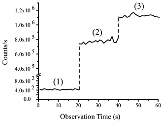
First, we observe the fluorescence of MOT atoms around the nanofiber. Fluorescence photons are measured by using an avalanche photodiode (Perkin Elmer, SPCM-AQR/FC) connected to one end of the fiber. Signals are accumulated and recorded on PC using a photon-counting PC-board (Hamamatsu, M8784). Observed photon counts are plotted in Fig. 2 for three conditions. During the first 20 seconds of observation both MOT beams and MOT magnetic-fields are switched off and the observed 400 counts/s is due to room-light scattering and dark counts of the detector. During the next 20 seconds MOT beams are switched on and the observed 8105 counts/s corresponds to scattered light from MOT laser beams coupled to the guided mode of nanofiber. During the final 20 seconds the MOT magnetic-fields are switched on and MOT is overlapped to the nanofiber. An increase of 3105 counts/s above the scattering background is clearly observed.
Fluorescence photon count is estimated as , where is effective number of atoms, atomic scattering rate, averaged coupling efficiency of spontaneous emission to the guided mode, fiber transmission from the mid to the one end, and detector quantum efficiency. and are 65 % and 45 %, respectively. For the total laser intensity of 63.3 mW/cm2 and the detuning of 10 MHz, the atomic scattering rate is calculated to be 5.2106 s-1 with a saturation intensity of 2.5 mW/cm2 and spontaneous emission lifetime of 30 ns. Assuming an effective observation volume around the nanofiber of 200 nm thickness hollow cylinder with 2 mm length, and are estimated as and %, respectively. Thus, we obtain the fluorescence photon count to be counts/s, which is in good agreement with the observed value.
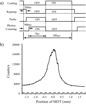
Next, we discuss the cold atom fluorescence measurements with a probe laser beam. The observations are performed following the time sequence shown in Fig. 3(a). When MOT has become ready, the cooling beam is switched off first, and the repumping beam is switched off 200 ns later so that all the atoms can be optically pumped into the hyperfine ground state. After switching off the repumping beam, the probe beam is switched on and the photon counting is started. The time interval between cooling-beam-off and photon-counting-on is 900 ns. The probe beam is irradiated perpendicularly to the nanofiber in a standing wave configuration to minimize resonant photon kick on the atoms, and the beam diameter is chosen to be 2 mm, just covering all the MOT atoms and the uniform nanofiber region. The polarization of the probe is linear and is perpendicular to the nanofiber axis. Photons are counted for 10 s. Then again the probe beam is switched off and the MOT beams are switched on for 190 s to recollect atoms into MOT. In this way the observation is repeated at a rate of 5 kHz and photon counts are accumulated for many cycles.
Figure 3(b) shows the observed photon count as a function of MOT position with respect to nanofiber. MOT position is scanned across the nanofiber in vertical direction. The probe laser frequency is tuned to the resonance of transition and the laser intensity is 3.3 mW/cm2. It is readily seen that scattering background has been greatly reduced compared to the value when the MOT beams are on; the value is 2.5103 counts/s. The spatial profile of MOT is clearly observed with a good S/N ratio. The observed profile is slightly asymmetric. We have fitted the profile with a Gaussian profile and obtained -diameter of 1.1 mm which well corresponds to the value of CCD measurement.
Regarding the observed fluorescence-photon-count, the peak value is 1.5 104 counts/s, which is about 1/20-times of that for the MOT observation in Fig. 2. We estimate the average number of atoms in the observation volume from the peak value using the same relation as for the MOT case. The number of atoms turns out to be a very small value of , which is 70 times smaller than the number for the MOT case. We have measured the temporal behavior of the peak value by setting the dark period much longer. Decay time is about 4 ms, which is well explained by the free expansion of the MOT cloud. These observations mean that the number of atoms in the observation region has quickly dropped to such small number during the time interval of 900 ns between switching off the cooling beam and starting the photon-counting outline .
Present observations have clearly demonstrated the peculiar feature of the nanofiber method to detect single atoms quite sensitively. The sensitivity is due to two factors. One is the high coupling efficiency of fluorescence photons to the guided mode. The other is that the nanofiber is immune to the scattering from irradiating light. When we irradiate the probe beam on the nanofiber, we readily observe bright light scattering from the nanofiber through a CCD camera. Irradiating photon flux on the nanofiber is estimated to be 2.31011 photons/s. Ideally speaking, however, such scattered radiations cannot be coupled into the guided mode of the nanofiber, since they are all in radiation modes and are orthogonal to the guided mode. As seen in Fig. 3(b), we do not observe any strong scattering radiations through the fiber; the observed scattered photon count through the fiber guided mode is very small, 2500 counts/s, which corresponds to a scattering probability of 3.710-8. In this meaning, the present nanofiber works almost ideally. Observed scattered photons might be due to some surface irregularities of the nanofiber induced during the nanofiber production and also by dusts on the surface. Such scattering may be reduced much more with further technical advancement.
We measure the fluorescence excitation spectrum of atoms around the nanofiber by scanning the probe laser frequency around the resonance (). Observed spectrum is displayed in Fig. 4(a) for three intensities of probe laser. The observed line shape is quite different from usual atomic line shape. Apparent power dependences (broadenings) are not observed, implying that the spectrum is not due to an isolated atomic spectrum, but consists of many spectral lines overlapped each other within spontaneous linewidth. The spectrum reveals a long tail in the red detuned side and consists of two peaks. One peak is almost on the atomic resonance and shows a small red tail. The other peak locates around the detuning = -30 -50 MHz and shows a long red tail up to = -140 MHz. Obviously, these observations are attributed to van der Waals (vdW) interaction between Cs-atom and nanofiber surface which would be dominant for distances closer than from the surface. Since we are observing atoms close to the nanofiber surface, appearance of the vdW interaction should be one of the natural consequences.
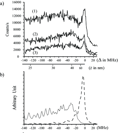
The surface induced red shift of atomic resonance is formulated as , where is distance of atom from the surface Ducloy . Using a parameter MHz for Cs-atom and glass surface Ducloy , we calibrate the detuning as an atom position from the surface as shown in Fig. 4(a). It implies that one can observe atoms which pass through some specific distance from the nanofiber by precisely tuning the probe laser frequency.
In order to clarify the observed spectral shape deeply, we calculate the eigenstates of the center-of-mass motion of the atom in a close vicinity of the nanofiber using known parameters for vdW potential for Cs-atom and silica surface vW-potential . Calculations are done for ground and first excited electronic states FC-factors . As discussed in Ref. Oria , the eigenstates are essentially analogous to molecular vibrational states. We calculate the Franck-Condon factors between ground and excited states and simulate the observable spectral profiles. Regarding the highest bound states, we included up to vibrational states with wavefunction turnig-point of nm. Simulations are carried out for two types of transitions. One is for the transitions from ground free-atomic states to the bound vibrational states for the excited vdW potential. This transition corresponds to photoassociation process; free atoms coming close to the nanofiber transit to the upper bound molecular states, where molecule consists of nanofiber and Cs-atom. The other is for transitions from bound ground vibrational states to bound excited vibrational states. The simulated photoassociation spectral profile is shown in Fig. 4(b) by a dashed plot. The profile is calculated for atoms with velocity distribution for 400 K. Upper vibrational states are taken for all possible transitions. The profile is almost on the atomic line with small red tail. Spectral profile for the ground vibrational to excited vibrational states is shown in Fig. 4(b) by a dotted plot. We calculate the profile assuming equal population distribution for ground vibrational states down to a binding energy of 200 MHz. The profile reveals a long red tail with a small offset peak position in the red side. The profile includes more than 100 spectral lines, which are overlapped each other within spontaneous spectral width FC-factors . We reproduce the observed spectrum with good correspondence by adding the photoassociation and the bound to bound profiles with adjusting the relative ratio. Thus we assign the observed red shaded peak on the atomic line as the photoassociation process and the other broad spectrum as due to the bound to bound vibrational transitions for atoms in the vdW potential.
In summary, we have demonstrated how optical nanofibers can manipulate and probe single-atom fluorescence. We have shown that very small number of atoms, average atom number of 0.07, around the nanofiber are detected with a good S/N ratio through single mode optical fiber under strong resonant laser irradiation. This is essentially due to the particular feature of the optical nanofiber around which an appreciable amount of atomic fluorescence is emitted into the fiber guided mode. The present results imply various possible applications, such as single-photon generation in optical fiber or EIT-based parametric four-wave mixing EIT-NLO using a few atoms around optical nanofibers, which may be of importance in the context of implementing quantum information technologies. Other than the above, the optical nanofiber may have further potential. Regarding the spatial-resolution of atom detection, we should mention that it may be in sub-micrometer scale, since observed fluorescence photons are only from near surface vdW region as discussed for the excitation spectrum. This high spatial resolution may induce some unique applications in atom optics. The inherent nature of the nanofiber method to detect vdW interaction between atoms and surface may open new possible directions to investigate atom-surface interaction with high precision. The optical nanofiber method can naturally be extended to other systems than atoms, like molecules or quantum-dots.
This work was carried out under the 21st Century COE program on Coherent Optical Science.
References
- (1) Also at Institute of Physics, National Center for Natural Sciences and Technology, Hanoi, Vietnam.
- (2) L. Tong et al., Nature (London) 426, 816 (2003).
- (3) S. G. Leon-Saval et al., Opt. Express 12, 2864 (2004).
- (4) M. Sumetsky et al., Opt. Express 12, 3521 (2004); M. Sumetsky et al., J. Lightw. Technol. 24, 242 (2006).
- (5) Fam Le Kien et al., Phys. Rev. A 72, 032509 (2005).
- (6) Fam Le Kien et al., Phys. Rev. A 72, 063815 (2005).
- (7) V. I. Balykin et al., Phys. Rev. A 70, 011401(R) (2004); Fam Le Kien et al., Phys. Rev. A 70, 063403 (2004).
- (8) M. Sumetsky, Opt. Lett. 31, 870 (2006).
- (9) Detailed dynamics is discussed elsewhere. The outline is as follows. Stationary atom number in the observation region is determined by a balance between atom loading to the region and loss in the region. Atoms in the region may finally be adsorbed to the nanofiber surface or reflected back from the surface. Both processes act as the loss processes in the observation region. Regarding the atom loading, the rate may be much higher with MOT than without MOT beams, because atoms in MOT are forced to direct toward the trap center due to friction force through cooling beam, whereas atoms without MOT beams are free and simply enter into the observation region just through diffusion process.
- (10) M. Oriá et al., Europhys. Lett. 14, 527 (1991); M. Chevrollier et al., Opt. Lett. 16, 1879 (1991).
- (11) W. R. Johnson et al., Phys. Rev. A 69, 022508 (2004).
- (12) Fam Le Kien et al., quant-ph/0610067; quant-ph/0610068.
- (13) E. G. Lima et al., Phys. Rev. A 62, 013410 (2000); T. Passerat de Silans et al., Appl. Phys. B 82, 367 (2006).
- (14) D. A. Braje et al., Phys. Rev. Lett. 93, 183601 (2004); V. Balić et al., Phys. Rev. Lett. 94, 183601 (2005); A. T. Black et al., Phys. Rev. Lett. 95, 133601 (2005).