Towards quantum computing with single atoms and optical cavities on atom chips
Abstract
We report on recent developments in the integration of optical microresonators into atom chips and describe some fabrication and implementation challenges. We also review theoretical proposals for quantum computing with single atoms based on the observation of photons leaking through the cavity mirrors. The use of measurements to generate entanglement can result in simpler, more robust and scalable quantum computing architectures. Indeed, we show that quantum computing with atom-cavity systems is feasible even in the presence of relatively large spontaneous decay rates and finite photon detector efficiencies.
1 Introduction
Quantum information processing (QIP) is a new paradigm for manipulating information. Already, in a first important application of QIP, quantum cryptography [5, 6] guarantees the physically secure transfer of information between distant parties. As for computing, algorithms have been devised that lead to a dramatic increase in computational speed when compared to the best known classical methods [1]. Prominent examples are Shor’s factoring algorithm [2] and Grover’s database search [3]. If a large-scale quantum computer were to be realised, with thousands of universal gates, no doubt more algorithms would emerge. However, even tens of qubits would be enough to provide a powerful computational platform for simulating specific quantum systems [4] whose complete Hilbert space is beyond the reach of current digital computers.
Many different physical implementations of QIP are currently being explored. Over the last few years, several proof-of-principle experiments have demonstrated the feasibility of quantum computing. Vandersypen et al. [7] have realized a simple instance of Shor’s algorithm by factoring using nuclear magnetic resonance techniques. Groups in Innsbruck and Boulder have implemented a universal two-qubit gate in an ion trap and entangled up to eight ions [8, 9]. Walther et al. have performed linear optics experiments with up to five photonic qubits and a four-photon cluster state [10]. However it is not straightforward to scale any of these to many more qubits. Additional qubits in ion traps increase the density of motional states, thereby creating the need for a form of distributed quantum computing, possibly involving ion transport [11]. As for linear optics quantum computing, the main difficulties when entangling photons are the lack of an effective interaction and the lack of reliable photon storage. For a recent comparative review of a number of quantum computing implementation proposals we refer the reader to Meter and Oskin [12].
Neutral atoms can be coupled to each other by the quantised field inside an optical cavity. Although not yet demonstrated experimentally, this offers a promising alternative implementation of quantum computing. It has already been shown that single atoms held in optical resonators are capable of generating single photons on demand and deterministically, i.e. without spontaneous emission[13, 14]. It is therefore possible to exchange quantum information between a stationary qubit (the atom) and a flying qubit (the photon), as required by one of DiVincenzo’s criteria for a scalable quantum computing architecture [15]. This may be used to couple distant parts of a quantum computer by generating photons whose state depends on the state of the respective atom [16] followed by carefully designed photon measurements [17, 18].
Photon measurements provide a very efficient tool for manipulating information in atom-cavity systems. They can be used to simplify significantly the production of entanglement. One example of that is the method based on an environment-induced quantum Zeno effect [20, 21, 22, 23], where the application of laser fields suffices to entangle two ground-state atoms trapped inside an optical cavity. A second approach due to Lim et al. [18] entangles distant atoms by the deterministic generation of photon pairs and their subsequent detection. As a third example, we recently we showed that the absence macroscopic fluorescence [27] can signal the presence of maximally entangled atom pairs [24] and may be used for the successive build-up of cluster states [25] for one-way quantum computing [26]. Such a signal can easily be detected even when using inefficient photon detectors.
Over the last few years, much progress has been made in observing and controlling the electronic and motional states of atoms inside optical resonators, including a variety of transport [28, 29], cooling [30] and trapping [14, 31] mechanisms. For most purposes, the quality of the atom-cavity system is measured by the relative sizes of the atomic decay rate , the atom-cavity coupling constant , and the cavity decay rate . The latter are given by [32]
| (1) |
where is the transition dipole moment and and are the length and the finesse of the Fabry-Perot resonator, respectively. For reflectivities , the finesse can be approximated by . Often, the quality of a resonator is given using the Q-factor, in terms of which . The ratio is known as the single-atom cooperativity parameter. This parameter is of central importance in atom detection, in single-photon production, and in the generation of entanglement between atoms sharing a cavity mode. After several years of steady progress in atom-cavity experiments, values of on the order of have been achieved [33, 34]. By measuring a classical fluorescence signal caused by quantum jumps, as suggested by Metz et al. [24], it should be possible to entangle two atoms with a fidelity above even when is as low as 10 and when detecting photons with an efficiency as low as .
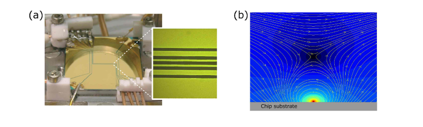
Atom chips can be manufactured to provide arrays of miniature traps and guides, allowing for the simultaneous trapping and manipulation of a large number of spatially separated single atoms [35]. Fig. 1 (a) shows an atom chip with wires fabricated in a gold film. The magnetic fields effected by current carried by these wires is used to manipulate Bose-Einstein condensates for atom interferometry [19]. As demonstrated recently [36, 37, 38], optical cavities that can be integrated into atom chips promise large cooperativity parameters due to their small mode volume. Moreover, neutral atoms are strong candidates for stationary qubit carriers as they interact only weakly with the environment and possess long decoherence times. For example, the lifetime of the coherence between the and hyperfine levels of the ground state of 87Rb has been measured to exceed one second, even when the atoms are held close to the surface of an atom chip in a magnetic microtrap [39]. Using silicon as the substrate material means furthermore that all necessary classical control circuits can be created on the same chip, leading to a fully integrated device. Atom-cavity systems on atom chips therefore hold great promise for scalable quantum computing in the near future.
In this article we report on recent efforts towards quantum computing with single atoms using optical cavities on atom chips. In this setup the successful completion of a quantum-logical gate operation can be heralded either by the deterministic generation and detection of single photons, the absence of single photon emissions or the absence of a macroscopic fluorescence signal. Two cavities, when combined with a reliable transport mechanism such as the magnetic guides and traps implemented on atom chips, are then sufficient to carry out quantum-computational operations on a large number of qubits. In Sections 2 and 3 we give a brief description of the methods used to trap atoms above an atom chip and report on recent achievements in combining such systems with optical resonators. In Sections 4 and 5 we review recent atom-cavity quantum computing proposals based on the measurements of photons leaking through the resonator mirrors. Finally, we summarise our results in Section 6.
2 Guiding and trapping single atoms
Atom chips are devices with micro-structured surfaces, which produce magnetic and/or electric fields and enable the trapping, cooling and manipulation of atomic clouds and single atoms. The magnetic fields are produced by current-carrying wires or permanently magnetised surfaces and couple to the magnetic dipole moment of the atoms. The small scale of the structure produces strong magnetic field gradients which make tight traps for magnetic atoms [35]. Figure 1(b) shows the field of a single wire (shown as a dot) to which a uniform bias field has been added. This creates a zero of the magnetic field above the wire, surrounded by a region of approximately quadrupole asymmetry. Atoms in a weak-field-seeking state will be attracted and held in this region. At a zero of the magnetic field, the weak- and strong-field-seeking states of the atom are degenerate, so a transition may occur which would lead to repulsion of atoms from the trap. To avoid this, a uniform field can be added parallel to the wire [40, 41].
Losses can still occur, for example because of current noise caused by thermal fluctuations, though these can be controlled by a suitable choice of material and film thickness [42, 43]. The lithographic process involved in creating the wires or permanent-magnetic structures makes it possible to create complex patterns repeatably and with high precision, which in turn guarantees the scalability of these components. The wires on atom chips have typical widths of to m and thicknesses of to m, and can carry currents on the order of to A. This makes it possible to form strong and tight traps, with trap frequencies on the order of kHz and depths on the order of mK. Similar trap characteristics have been obtained with micro-patterned permanent-magnetic surfaces [40]. Wires patterned using UV-lithography have edges with a feature size of less than nm and with a surface roughness of less than nm. This is important to ensure that electrical currents flow smoothly along the wires, thereby creating a uniform trap for the atoms [44]. The atoms still need to be pre-cooled before they can be loaded into these traps, and this is usually done in a magneto-optical trap close to the surface of the chip.
3 Integrating optical cavities
Until recently, atom chip experiments have focussed on trapping and manipulating large clouds of atoms, with a view to creating Bose-Einstein condensates (BECs) [45, 41, 40]. However, the reliable delivery and individual control of single cold atoms, each of them carrying one qubit, is a necessity for many quantum computing schemes. To achieve this, it must first be possible to detect single atoms with a high degree of confidence [46]. Furthermore, as mentioned in the Introduction, the coupling of atoms to the field of an optical cavity is a powerful tool for entangling them, and the strength of this coupling increases with decreasing cavity mode volume. The inherently small mode volume of a microcavity therefore provides a strong incentive for the use of such a device for quantum optics experiments. Atom chip circuits enable the positioning of atoms with high accuracy down to the sub-nanometer scale [47]. This is an important tool in the attempt to couple atoms stably and accurately to the modes of micro-resonators.
Two types of resonator are being integrated with atom chip technology: whispering-gallery-mode (WGM) [48, 49, 47, 50, 38] and Fabry-Perot (FP) microcavities [47, 19]. WGM cavities have unprecedented quality factors, with the best microsphere resonators approaching [48]. However, because the intense part of the mode is confined within the solid material of the resonator, coupling to the mode has to be made through the weaker evanescent field outside. The latter decreases exponentially with distance from the resonator surface, with a decay constant of order . For an atom to interact perceptibly with the resonator mode it must therefore be placed accurately, i.e. to within a small fraction of a wavelength, in close proximity of the resonator surface, where the attractive Van der Waals force on the atom becomes considerable.
A number of WGM devices have been proposed as candidate systems for the detection and manipulation of atoms. Fused-silica microspheres have the highest known quality factors, but the procedure used for fabricating them is not easily included in the production of atom chips. Such a resonator would have to be positioned on the surface and attached to the atom chip using procedures separate from the standard etching and coating steps used in the manufacture of semiconductor chip devices. Furthermore, the dimensions and quality of microspheres vary considerably from one to another [48]. Microtoroids are therefore more natural candidates for integration as they can be produced using standard microfabrication techniques, and still offer very high quality factors [51]. Strong coupling between single atoms and the field of a microtoroid resonator has in fact been demonstrated recently [38], albeit with atoms passing through the evanescent field in free-fall. While the strong-coupling condition has been experimentally fulfilled for the first time for a WGM device, the challenge of reliably positioning atoms in the evanescent field with the required accuracy has yet to be surmounted.
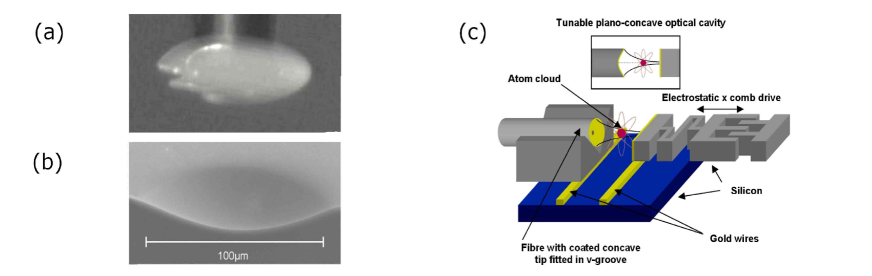
By contrast, FP resonators have lower values of finesse and . However, atoms can be placed directly and accurately into the region of highest field strength of the cavity mode, leading in practice to higher values of that are reproducible. Furthermore the requirements on positional accuracy of the atoms within the mode are less stringent because the intensity varies slowly near the antinodes, with a standing wave spacing of and a mode waist of m. For these reasons, the efforts of several research groups are currently focussed on this type of resonator. One type of FP-microcavity, currently in use at Imperial College London, is a plano-concave resonator consisting of an isotropically etched dip in a silicon surface and the cleaved tip of a single-mode fibre [36]. Figure 2 (a) is a picture taken under an optical microscope of the coated fibre tip. Initially, the reflecting film is formed by evaporating onto a donor surface to which it is weakly attached. The fibre tip is then aligned to this surface, and glued firmly to the reflective coating using a UV-curing, index-matching epoxy. Pulling the fibre away from the donor surface completes the procedure. This abrupt detachment is the cause of the rough edges visible in Figure 2 (a), but does not damage the reflecting surface. Figure 2 (b) is a scanning electron microscope image of the curved silicon mirror substrate. The image shows a specimen which has been cleaved close to the centre to make the curvature more readily discernible. This surface was also subsequently coated with a high-reflectivity multilayer dielectric film using a standard sputtering procedure. A finesse in excess of and a Q-factor of over have been achieved with cavities of this type. These values are limited by scattering losses caused by the surface roughness of the silicon mirror substrate, which is approximately nm rms. This can be improved upon by adding a deep reactive ion etching step, or by depositing and thermally reflowing a layer of silica before applying the mirror coating. The present performance values are nonetheless sufficient in principle to detect single atoms with high confidence, and should also enable the generation of single photons with high efficiency. This method of making concave mirrors relies on standard silicon etching and coating techniques and is easily included in the chip fabrication procedure. The formation of the microcavity then only requires the positioning of the coated fibre tip above the chip surface, without the need for further coupling optics. However, the cavity still needs to be tuned by an external piezoelectric actuator. The next generation of microcavity will be built on the chip surface in a planar orientation and will be tuned by an integrated electrostatic actuator [52].
Several experimental groups have already succeeded in positioning atoms accurately within the mode of an optical resonator using optical [14, 29], electrostatic [53, 54] and magnetic [55, 56] transport techniques. The positioning of atoms by means of magnetic guides in a microcavity on a chip has also been recently demonstrated using a fibre-coupled microcavity [37]. Both mirrors of that microcavity are fibre tips to which concave multilayer dielectric coatings have been applied using a transfer procedure similar to the one described above, but using a convex donor surface. The highest finesse achieved with this type of microcavity is on the order of , limited by mirror roughness. An improved construction uses two fibres with laser-machined concave tips. They are extremely smooth because the curvature is created by evaporation, which allows the surface to reflow smoothly as it is formed. This results in a surface roughness of less than nm rms. A high-reflection multilayer dielectric coating is then applied to the tips, giving a finesse of , and a remarkable theoretical single-atom cooperativity of over .
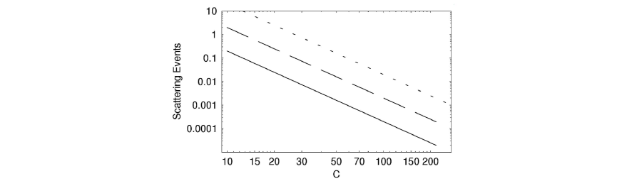
The presence of an atom in the mode of a resonator can drastically alter its transmission and reflection properties. In microcavities such as those described above, this effect is large enough to allow the detection of single atoms with high confidence even for modest finesse values [46, 38]. This quality alone is already of interest for atom-chip experiments as it can be used to measure in situ the performance of single-atom transport and positioning mechanisms available on atom chips. However, beyond the initial objective of detecting single atoms, it is desirable for QIP purposes that both the kinetic and internal states of the atom be preserved beyond the detection event. Microcavities currently available for atom chips should allow atoms to be detected while keeping the excitation probability far below unity. For example, with a weakly pumped system driven on resonance, the number of scattering events expected to occur during the detection process in a microcavity with is given by [46]
| (2) |
Here is the signal-to noise ratio and is the detection efficiency of the system. The latter includes both the quantum efficiency of the photon detector and losses that occur at any point after the interaction of the photons with the atom. The solid line in Figure 3 shows the number of scattering events that will occur if the detection efficiency is perfect and the signal-to-noise ratio is 10. Also shown are curves for 10% and 1% detection efficiencies. In the atom-cavity systems described above, the primary sources of loss are the roughness of the mirror surfaces and the mode overlap between the fibre mode and the resonator mode. Minimising these losses is of the utmost importance not only for the confident detection of single atoms, but also for the efficiency of more intriguing applications, such as the deterministic generation of single photons on demand.
4 Single photon sources for QIP
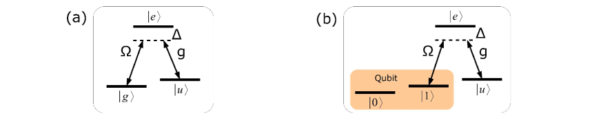
Atom-cavity systems such as those presented above have sufficiently high cooperativity to generate single photons on demand[13, 14]. For this to occur deterministically, it must be possible to position a single atom at a maximum of the cavity mode. The relevant atomic level configuration is shown in Figure 4(a). The system is initially prepared with the atom in state and no light in the cavity. A cavity photon is then generated by applying a laser beam with increasing Rabi frequency , as shown in Fig. 4(a), in order to drive a stimulated Raman transition [13]. This takes the atom adiabatically from to without creating any significant population of the excited state , thereby coherently scattering a single photon from the laser field into the cavity mode. This photon subsequently leaks out of the cavity through the output coupling mirror.
Single-photon sources have many potential applications in QIP. One is the generation of entangled multi-photon states [57] for linear optics quantum computing [58], where each qubit is encoded in a photon and gate operations are effected by measurements. Photonic qubits are attractive because they are easily distributed and all the required operations for quantum computing are based on existing technology. Currently, linear optics experiments rely on photon pairs produced by parametric down-conversion. Detection of one photon heralds the presence of the other with certainty, but still the arrival times are uncontrolled, making it necessary to store photons for substantial periods of time in order to build up states of several entangled photons. The current maximum number is five [10].
Beyond its use as a single-photon source, the atom-cavity system can form a link between stationary and flying qubits. If information is encoded in the internal states of the atomic sources [59, 17], two distant qubits can be coupled by photons generated in their respective cavities. A carefully designed photon-pair measurement, i.e. one which does not reveal any information about the individual sources, can then entangle the qubits deterministically, as proposed by Lim et al. [18]. Quantum computing using this scheme is scalable, even with only two cavities. It is possible to perform a universal two-qubit gate operation between any two atoms above an atom chip provided any atom can be moved at will into one of the resonators.
One atomic level configuration suitable for implementing this [18] is shown in Figure 4(b). Each qubit is encoded in two stable ground states, labelled and , of a single atom trapped inside an optical cavity. A comparison with Figure 4(a) shows that this level scheme can be operated as a source for the generation of single photons on demand. A photon can be created if the atom is initially prepared in , while the system cannot generate a photon if the state of the atom is . A laser pulse first swaps the states and , followed by an increasing laser pulse for the generation of a single photon on demand. If this process is repeated, a qubit initially prepared in becomes
| (3) |
where and denote an early and a late generated photon, respectively. This encoding step (3) entangles the qubit with a newly generated photon. A measurement on the photon therefore also affects the state of the atomic qubit.
If two atoms are initially prepared in an arbitrary two-qubit state of the form , then the encoding step (3) transforms the system according to
| (4) |
A suitably designed measurement then projects the photon pair into a state of the form , with the result
| (5) |
This final state differs from the initial state by a unitary phase gate. Performing a phase gate in a deterministic fashion therefore requires only photon-pair measurements, where each of the four possible measurement outcomes is an equal superposition of the states , , and . With linear optical elements alone, it is possible to perform these measurements on a basis of two maximally entangled states and two product states[18]. The detection of a maximally entangled photon state indicates the realisation of an entangling two-qubit phase gate on the atoms. This is equivalent to a controlled-Z gate up to local phase shifts. The detection of a product state, on the other hand, indicates the realisation of a local phase gate. Since the atomic qubits are not destroyed at any stage of the computation, the implementation of a desired universal entangling phase gate can be repeated until success.
Under realistic conditions, repeat-until-success quantum gates are less than successful because of photon loss. Nevertheless, the scheme of [18] can be used to build up cluster states [60, 61] with very high fidelity. The detection of a photon pair perfectly heralds the outcome of the gate operation on the atoms as long as dark counts are negligible. Two-dimensional cluster states constitute a very efficient resource for quantum computing. Once a cluster state has been built, a whole quantum computation can be performed using only single-qubit rotations and single-qubit measurements [26].
5 Atom-cavity schemes for QIP
Instead of entangling atoms in separate cavities, one could achieve entanglement with the atoms placed at two antinodes within the same cavity. This can be done coherently but dissipative processes, which are unavoidable in real resonators, are detrimental. As Zheng and Guo [62] have pointed out, when one tries to minimise spontaneous emission with the help of large detunings, this comes at the expense of slower gate operations. In the end the failure rate is independent of detuning and depends primarily on the single-atom cooperativity parameter . The scheme was nonetheless successfully implemented with Rydberg atoms flying through a high finesse cavity [67].
In order to lower the requirements on the cooperativity of atom-cavity systems, dissipation can be employed constructively for quantum gate operations by performing appropriate measurements on the system. The first example was the 1995 atom-cavity quantum computing scheme of Pellizzari et al. [63], based on a dissipation-assisted adiabatic passage [64]. A hybrid approach using dissipation in the form of an environment-induced quantum Zeno effect, whereby the evolution of the system is inhibited by frequent measurement, and adiabatic passages was suggested by Pachos and Walther [22]. They predict gate success rates above even for . This improvement comes at the expense of a relatively complex stimulated Raman adiabatic passage (STIRAP) entangling process. A related but simpler scheme by Yi et al. [23] achieves gate success rates above for . Most recently we have shown (see below) that even better performance can be achieved if the atoms are coupled resonantly to the cavity mode.
In the following, we summarise the scheme by Yi et al. [23], which achieves a controlled phase gate between two atoms trapped inside an optical cavity without having to address the atoms individually. A slight modification of the scheme [23] allows us to achieve gate success rates above even for . The scheme is based on a quantum Zeno effect combining ideas in Refs. [20, 22] and [23]. While the scheme by Lim et al. [18], discussed in Section 4, uses photon detections to impose an entangling gate operation, the same goal is now achieved by observing the absence of emissions. For , the quantum Zeno effect significantly reduces the probability for an emission to take place and schemes based on this effect therefore do not depend on having exceptionally efficient single-photon detectors. Nevertheless, the proposed scheme makes use of measurements to simplify the realisation of the gate.
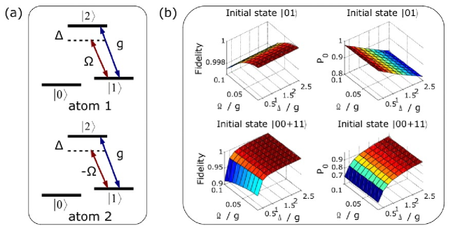
Suppose two atoms with a -like level configuration as shown in Figure 5(a) are simultaneously trapped inside an optical cavity. The 1–2 transition of each atom couples with the same coupling constant to the field mode inside the resonator. Then there exists a five-dimensional subspace whose population cannot emit a photon into the cavity. This subspace of so-called dark states is spanned by the qubit states , , , and the maximally entangled antisymmetric state
| (6) |
which does not couple to the cavity mode due to the symmetry of the state [20]. When prepared in , both atoms try to place excitation into the cavity field but interfere destructively so that neither of them succeeds.
If the atom-cavity coupling and the cavity decay rate are strong enough, then the observation of no photons leaking out through the cavity mirrors constitutes a continuous measurement of whether the system is in a dark state or not [20, 21]. The application of a weak perturbation under these conditions cannot move the system out of the decoherence-free subspace because the system evolves according to the effective Hamiltonian
| (7) |
where is the projector onto the dark states of the system,
| (8) |
To obtain the interaction , laser fields in any configuration could be applied, as long as their Rabi frequencies are sufficiently weak compared to and . The effective Hamiltonian (7) realises a quantum gate between the qubits if the timing is such that there is no population in at the end of the operation. One could for example implement a CNOT-gate by driving the 1–2 transition in atom 2 with a Rabi frequency and the 0–2 transition in atom 1 with a Rabi frequency [21]. However, it is also possible to perform two-qubit phase gates without addressing the atoms separately, as we now discuss. Furthermore, we can stay in the same parameter regime as in Ref. [22],
| (9) |
In the following, a laser field drives the 1–2 transition in atom 1 with Rabi frequency , while atom 2 is driven with the opposite phase to make a Rabi frequency of , as illustrated in Figure 5(a). The detuning can be used to control the population of excited state and thus to ensure low spontaneous emission out of the cavity, but there is no need to use it to avoid populating the cavity mode. In an appropriately chosen interaction picture, the interaction Hamiltonian can then be written as
| (10) |
Together with Eqs. (7) and (8), this yields the effective Hamiltonian
| (11) |
Given the parameter regime (9), the Hamiltonian (11) can be simplified further via an adiabatic elimination of the excited atomic state . This yields
| (12) |
where . The corresponding time evolution operator equals
| (13) |
and adds a minus sign to the state , if . A single laser pulse can therefore indeed be used to realise a controlled phase gate with a very high fidelity even in the presence of non-negligible spontaneous decay rates and .
This two-qubit gate has the advantage of being highly successful even for relatively moderate cavity parameters. Figure 5(b) shows the fidelity and success rate versus and of a controlled phase gate with for the initial states and . In particular, we see that the system is optimally operated using , thereby maximising both the fidelity and the no-photon probability. Using ideal photon detectors, it is possible to achieve gate fidelities well above under the condition of no photon emission, and gate success probabilities above . If the detectors are less efficient the gate fidelity decreases, but only to the level of the gate success rate.
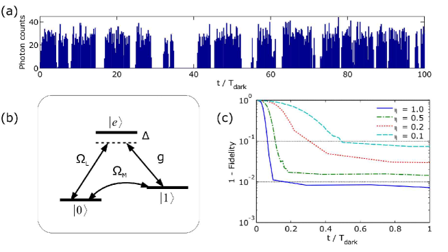
Recently, Metz et al. [24] proposed an alternative measurement-based scheme for the generation of a well-defined maximally entangled state of two atoms. Instead of deciding on the success of the operation by the absence or the detection of single photons, the scheme uses macroscopic light and dark periods [27], during which the system either emits no photons at all (dark period) or generates photons stochastically (light period). In the following, we consider a system designed such that macroscopic dark periods, like the ones in Figure 6(a), indicate the successful preparation of two atoms in a maximally entangled atomic ground state. Since a macroscopic dark period can easily be distinguished from a macroscopic light period, the scheme is expected to work reliably even when using imperfect photon detectors.
The telegraph signal in the fluorescence of a single quantum system was discussed as early as 1975 by Dehmelt in the context of electron shelving [27]. At that time, the origin of the underlying process raised many questions about our understanding of quantum mechanics. Nowadays it is well known that the interaction of the system with its environment effectively results in a measurement, thereby revealing information about the system. This projects it into a state which is characterised either by constant fluorescence or by its complete absence [65, 66].
Figure 6(b) shows the level configuration of a single atom. A system composed of two such atoms in a cavity is expected to exhibit macroscopic light and dark periods. Again, each qubit is obtained from the ground states and of an atom. The 1– transition couples with detuning to the cavity mode, while the 0– transition and the 0–1 transition are driven by fields with Rabi frequencies and , respectively. Given the parameter regime [24], the system possesses the dark state
| (14) |
In the presence of the driving fields, this state is the only one which does not emit photons into the cavity mode. The observation of a macroscopic dark period in the fluorescence of photons through the cavity mirrors therefore reveals the successful preparation of the atoms in (14). Switching off the driving fields is then sufficient to keep the system in this maximally entangled state.
Below we list the typical time scales considered, with denoting the mean time between photons during a light period, while and are the mean durations of light and dark periods, respectively. As shown in Ref. [24], they are given by
| (15) |
if . Here we have assumed for simplicity that the 0– and the 1– transition have the same spontaneous decay rates. The ratio of to is crucial for distinguishing a light from a dark period. Eq. (15) shows that it is possible to have almost 300 times as long as , even when the single-atom cooperativity parameter is as low as 40. Since and are of about the same size, one does not have to wait very long before the system assumes the desired state (14).
Figure 6(c) shows the fidelity of the state that is prepared if the laser field is turned off upon the detection of no photon for a time . Fidelities above are achievable even with a detector efficiency as low as and for the realistic cooperativity . This method is robust because it makes use of the dark periods of the telegraph signal. Instead of being a destructive effect, dissipation plays a key role in the protocol to generate entanglement. Work is currently underway to use macroscopic light and dark periods for the generation of cluster states for one-way quantum computing [25].
6 Conclusions
In Sections 2 and 3, we have reported on recent
developments in atom chip technology and have described the
integration of optical cavities into atom chips. Microcavities
currently available for this purpose have already successfully
detected single atoms, and are of sufficient quality to be used for
the generation of single photons on demand. Sections 4
and 5 outlined possible QIP experiments with single
atoms and pairs of atoms trapped in the field of optical cavities.
In all examples, atoms are entangled by measuring photons leaking
through the resonator mirrors. The successful completion of an
operation can be heralded by the detection of single photons, the
absence of photon emissions or the absence of a macroscopic
fluorescence signal. Using measurements to herald entanglement leads
to a considerable easing of experimental constraints and increases
the robustness and scalability of
quantum computing architectures.
Acknowledgement. A. B. acknowledges funding from the Royal Society and the GCHQ as a James Ellis University Research Fellow. This work was supported in part by the UK Engineering and Physical Sciences Research Council through its interdisciplinary Research Collaboration on Quantum Information Processing, and by the European Union Network SCALA.
References
- [1] D. Deutsch, Proc. R. Soc. A 400, 97 (1985).
- [2] P. W. Shor, ed. by S. Goldwasser, Proceedings of the 35th Annual Symposium on the Foundations of Computer Science, IEEE Computer Society, p. 124 (1994).
- [3] L. K. Grover, Phys. Rev. Lett. 79, 325 (1997).
- [4] R. P. Feynman, Internat. J. Theoret. Phys. 21, 467 (1982).
- [5] C. H. Bennett and G. Brassard, Proc. IEEE Int. Conf. Computers, Systems and Signal Processing, Bangalore, India, p. 175 (1984).
- [6] A. K. Ekert, Phys. Rev. Lett. 67, 661 (1991).
- [7] L. M. K. Vandersypen, M. Steffen, G. Breyta, C. S. Yannoni, M. H. Sherwood, and I. L. Chuang, Nature 414, 883 (2001).
- [8] D. Leibfried, E. Knill, S. Seidelin, J. Britton, R. B. Blakestad, J. Chiaverini, D.B. Hume, W. M. Itano, J. D. Jost, C. Langer, R. Ozeri, R. Reichle, and D. J. Wineland, Nature 438, 639 (2005).
- [9] H. Häffner, W. Hänsel, C. F. Roos, J. Benhelm, D. Chek-al-kar, M. Chwalla, T. Korber, U. D. Rapol, M. Riebe, P. O. Schmidt, C. Becher, O. Gühne, and R. Blatt, Nature 438, 643 (2005).
- [10] P. Walther, K. J. Resch, T. Rudolph, E. Schenck, H. Weinfurter, V. Vedral, M. Aspelmeyer, and A. Zeilinger, Nature 434, 169 (2005).
- [11] D. Kielpinski, C. Monroe, and D. J. Wineland, Nature 417, 709 (2002).
- [12] R. V. Meter and M. Oskin, J. Emerg. Technol. Comput. Syst. 2, 1 (2006).
- [13] A. Kuhn, M. Hennrich and G. Rempe, Phys. Rev. Lett. 89, 067901 (2002).
- [14] J. McKeever, A. Boca, A. D. Boozer, R. Miller, J. R. Buck, A. Kuzmich and H. J. Kimble, Science 303, 1992 (2004).
- [15] D. P. DiVincenzo, Fortschritte der Phys. 48, 771 (2000).
- [16] B. B. Blinov, D. L. Moehring, L.-M. Duan, and C. Monroe, Nature 428, 153 (2004).
- [17] I. E. Protsenko, G. Reymond, N. Schlosser, and P. Grangier, Phys. Rev. A 66, 062306 (2002).
- [18] Y. L. Lim, A. Beige, and L. C. Kwek, Phys. Rev. Lett 95, 030505 (2005).
- [19] S. Eriksson, M. Trupke, H. F. Powell, D. Sahagun, C. D. J. Sinclair, E. A. Curtis, B. E. Sauer, E. A. Hinds, Z. Moktadir, C. O. Gollasch, and M. Kraft, Eur. Phys. J. D 35, 135 (2005).
- [20] A. Beige, D. Braun, B. Tregenna, and P. L. Knight, Phys. Rev. Lett. 85, 1762 (2000).
- [21] B. Tregenna, A. Beige, and P. L. Knight, Phys. Rev. A 65, 032305 (2002).
- [22] J. Pachos and H. Walther, Phys. Rev. Lett. 89, 187903 (2002).
- [23] X. X. Yi, X. H. Su, and L. You, Phys. Rev. Lett. 90, 097902 (2003).
- [24] J. Metz, M. Trupke, and A. Beige, arXiv:quant-ph/0510051 (2005).
- [25] J. Metz, C. Schön, and A. Beige (in preparation).
- [26] R. Raussendorf and H. J. Briegel, Phys. Rev. Lett. 86, 5188 (2001).
- [27] H. G. Dehmelt, Bull. Am. Phys. Soc. 20, 60 (1975).
- [28] J. A. Sauer, K. M. Fortier, M. S. Chang, C. D. Hamley, and M. S. Chapman, Phys. Rev. A 69, 051804 (2004).
- [29] S. Nußmann, M. Hijlkema, B. Weber, F. Rohde, G. Rempe, and A. Kuhn, Phys. Rev. Lett. 95, 173602 (2005).
- [30] S. Nußmann, K. Murr, M. Hijlkema, B. Weber, A. Kuhn, and G. Rempe, Nature Physics 1, 122 (2005).
- [31] P. Maunz, T. Puppe, I. Schuster, N. Syassen, P. H. W. Pinkse, and G. Rempe, Nature 428, 50 (2004).
- [32] A. Kuhn and G. Rempe, Optical Cavity QED: Fundamentals and Application as a Single-Photon Light Source, Int. School of Physics Enrico Fermi, Course CXLVIII, edited by F. De Martini and C. Monroe IOS, Amsterdam, 2002, pp. 3766.
- [33] J. A. Sauer, K. M. Fortier, M. S. Chang, C. D. Hamley, and M. S. Chapman, Phys. Rev. A 69, 051804(R) (2004).
- [34] P. Maunz, T. Puppe, I. Schuster, N. Syassen, P. H. W. Pinkse, and G. Rempe, Phys. Rev. Lett. 94, 033002 (2005).
- [35] R. Folman, P. Krüger, J. Schmiedmayer, J. Denschlag, and C. Henkel, sAdv. At. Mol. Phys. 48, 263 (2002). E A Hinds and I G Hughes, J. Phys. D: Appl. Phys. 32 (1999).
- [36] M. Trupke, E. A. Hinds, E. Eriksson, E. A. Curtis, Z. Moktadir, Z. Kukharenka, and M. Kraft, Appl. Phys Lett. 87, 211106 (2005).
- [37] P. Treutlein, T. Steinmetz, Y. Colombe, B. Lev, P. Hommelhoff, J. Reichel, M. Greiner, O. Mandel, A. Widera, T. Rom, I. Bloch, and T. W. Hänsch, arXiv:quant-ph/0605163 (2006).
- [38] T. Aoki, B. Dayan, E. Wilcut, W. P. Bowenb, A. S. Parkins, and H. J. Kimble, arXiv:quant-ph/0606033 (2006).
- [39] P. Treutlein, P. Hommelhoff, T. Steinmetz, T. W. Hänsch, and J. Reichel, Phys. Rev. Lett. 92, 203005 (2004).
- [40] C. D. J. Sinclair, E. A. Curtis, I. Llorente-Garcia, J. A. Retter, B. V. Hall, S. Eriksson, B. E. Sauer, and E. A. Hinds, Phys. Rev. A 72, 031603 (2005).
- [41] J. Reichel, Appl. Phys. B 74, 469 (2002).
- [42] M. P. A. Jones, C. J. Vale , D. Sahagun-Sanchez, B. V. Hall, and E. A. Hinds, Phys. Rev. Lett. 91, 080401 (2003).
- [43] P. K. Rekdal, S. Scheel, P. L. Knight, and E. A. Hinds, Phys. Rev. A 70, 013811 (2004).
- [44] P. Kruger, L. M. Andersson, S. Wildermuth, S. Hofferberth, E. Haller, S. Aigner, S. Groth, I. Bar-Joseph, and J. Schmiedmayer, ArXiv:cond-mat/0504686 (2005).
- [45] M. H. Anderson, J. R. Ensher, M. R. Matthews, C. E. Wieman, and E. A. Cornell, Science 269, 198 (1995).
- [46] P. Horak, B. G. Klappauf, A. Haase, R. Folman, J. Schmiedmayer, P. Domokos, and E. A. Hinds, Phys. Rev. A 67, 043806 (2003).
- [47] R. Long, T. Steinmetz, P. Hommelhoff. W. Hänsel, T.W. Hänsch, and J. Reichel, Phil. Trans. Roy Soc. Lon. A 361, 1375 (2003).
- [48] J. Ye, D. W. Vernooy, and H. J. Kimble, Phys. Rev. Lett. 83, 4987 (1999).
- [49] M. Rosenblit, P. Horak, S. Helsby, and R. Folman, Phys. Rev. A 70, 053808 (2004).
- [50] Y. Louyer, D. Meschede, and A. Rauschenbeutel, Phys. Rev. A 72, 031801 (2005).
- [51] K. J. Vahala, Nature 424, 839 (2003).
- [52] C. Gollasch et al., to be published (2006).
- [53] G. R. Guthöhrlein, M. Keller, K. Hayasaka, W. Lange, and H. Walther, Nature 414, 49 (2001).
- [54] A. Kreuter, C. Becher, G. P. T. Lancaster, A. B. Mundt, C. Russo, H. Häffner, C. Roos, J. Eschner, F. Schmidt-Kaler, and R. Blatt, Phys. Rev. Lett. 92, 203002 (2004).
- [55] I. Teper, Y. Lin, and V. Vuletić, arXiv:cond-mat/0603675 v1
- [56] A. Haase, B. Hessmo, and J. Schmiedmayer, Opt. Lett. 31, 268 (2006).
- [57] A. Beige, Y. L. Lim, and C. Schön, arXiv:quant-ph/0602038 (2006).
- [58] E. Knill, R. Laflamme, and G. J. Milburn, Nature 409, 46 (2001).
- [59] J. I. Cirac, A. K. Ekert, S. F. Huelga, and C. Macchiavello, Phys. Rev. A 59, 4249 (1999).
- [60] S. D. Barrett and P. Kok, Phys. Rev. A 71, 060310(R) (2005).
- [61] Y. L. Lim, S. D. Barrett, A. Beige, P. Kok, and L. C. Kwek, Phys. Rev. A 73, 012304 (2006).
- [62] S.-B. Zheng and G. C. Guo, Phys. Rev. Lett. 85, 2392 (2000).
- [63] T. Pellizzari, S. A. Gardiner, J. I. Cirac, and P. Zoller, Phys. Rev. Lett. 75, 3788 (1995).
- [64] C. Marr, A. Beige, and G. Rempe, Phys. Rev. A 68, 033817 (2003).
- [65] R. J. Cook and H. J. Kimble, Phys. Rev. Lett. 54, 1023 (1985).
- [66] G. C. Hegerfeldt, Fortschr. Phys. 46, 595 (1998).
- [67] S. Osnaghi, P. Bertet, A. Auffeves, P. Maioli, M. Brune, J. M. Raimond, and S. Haroche, Phys. Rev. Lett. 87, 037902 (2001).