Integrated Conditional Teleportation and Readout Circuit Based on a Photonic Crystal Single Chip
Durdu Ö. Güney
Department of Electrical and Computer Engineering, University of California, San Diego, 9500 Gilman Dr., La Jolla, California, 92093-0409
Department of Mathematics, University
of California, San Diego, 9500 Gilman Dr.,
La Jolla, California, 92093-0112
dguney@ucsd.edu
David A. Meyer
Department of Mathematics, University
of California, San Diego, 9500 Gilman Dr.,
La Jolla, California, 92093-0112
dmeyer@math.ucsd.edu
Abstract
We demonstrate the design of an integrated conditional quantum
teleportation circuit and a readout circuit using a two-dimensional
photonic crystal single chip. Fabrication and testing of the proposed
quantum circuit can be accomplished with current or near future semiconductor
process technology and experimental techniques. The readout part of
our device, which has potential for independent use as an atomic interferometer,
can also be used on its own or integrated with other compatible optical
circuits to achieve atomic state detection. Further improvement of
the device in terms of compactness and robustness could be achieved
by integrating it with sources and detectors in the optical regime.
OCIS codes: 020.5580, 220.4830, 230.5750, 230.7370, 270.1670, 270.5580.
1 Introduction
It has been shown theoretically by Bennett1, et al. that quantum teleportation of an unknown state can be achieved using Bell states. Since then several theoretical and experimental schemes have been proposed, which include implementation in optical, NMR, and cavity QED systems2-5. Inspired by the recent paper of S.-B. Zheng2, in this letter we propose a photonic crystal (PC) based cavity QED implementation of the scheme described therein, as well as the integration of the device with an atomic readout circuit to detect the teleported state. Since our proposed device functions as a very simple conditional teleportation chip, where the success of the protocol is conditioned on a specific measurement result contrary to unconditional one, it could be fabricated and tested with current or near future semiconductor processing technology and experimental techniques, respectively.
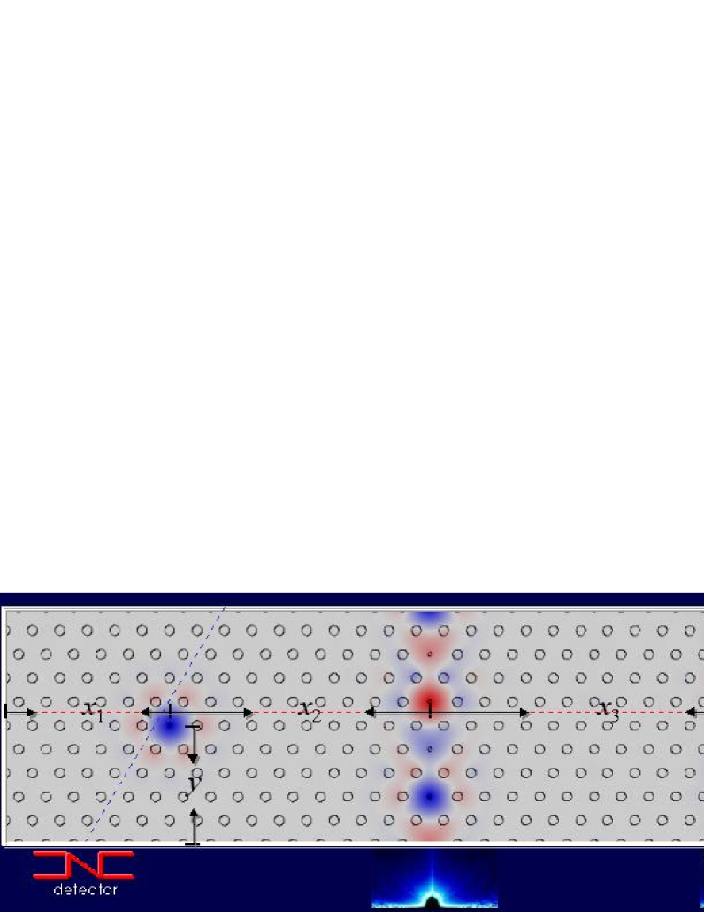
An illustration of the photonic crystal chip that we propose is shown in Fig. 1, where a single mode cavity is integrated with two parallel waveguides. The actual size of the chip, which is designed in this letter, is larger than that of the illustration. The actual height (i.e., vertical) is and the width (i.e., horizontal) is , where is the lattice constant. , , , and are , , , , and , respectively. Because of its large size, we design the chip in a 2D lattice to reduce the high computational cost of 3D crystal analysis. This is, however, a good approximation due to the ability of 2D photonic crystal defect modes to emulate those of 3D photonic crystals. This emulation issue is considered in detail in Ref. [6] and its advantages for photonic crystal based quantum logic gate design are discussed in Ref. [7], where we have used exactly the same lattice parameters. Thus, our 2D PC structure is chosen to emulate its 3D counterpart and is based on a triangular lattice of silicon rods with dielectric constant of and lattice constant of . The radii of the rods and the defects are and , respectively. The trajectories of the atoms through the PC are depicted by the red and blue dashed lines in Fig. 1.
Incorporated with detectors, the cavity part of the chip operates as a teleportation circuit and the parallel waveguides act as a readout circuit to detect the teleported atomic state (see Fig. 1). Below we use the terms, teleportation circuit (TC) and readout circuit (RC), respectively to refer those two integrated photonic crystal circuits. We choose the width of the former to be and the latter to be in order to avoid unwanted coupling between the two circuits. In the first part of this letter we describe the teleportation mechanism and in the second part we explain how to detect the atomic state8-11 within our designed PC quantum circuit (PCQC).
2 Teleportation Circuit
The TC involves the interaction of two Rb atoms with a resonant high-Q (assumed to be larger than to prevent cavity decoherence) single mode cavity and the detection of one of the atoms using a detector. The total Hamiltonian (Jaynes-Cummings Model) for the TC under the dipole and rotating wave approximations is given by7:
| (1) |
where the summation is carried over two atoms, and , is the resonant frequency, is the -component of the Pauli spin operator and are the atomic raising and lowering operators. and are the annihilation and creation operators, respectively. is the atom-cavity coupling parameter at the position of atom and can be written as
| (2) |
denotes the vacuum Rabi frequency and is the position in the dielectric where the electric field energy density is maximum. Note that we implicitly assume in Eq. (2) that the atomic dipole moments, , of the atoms are aligned with the photon polarization.
In the first stage of the conditional teleportation protocol, atom (whose trajectory is depicted by the red dashed line in Fig. 1), initially in the excited state , traverses the cavity, which is initially in the vacuum state , with velocity . Since at this stage atom , whose state is to be teleported, is not in play, index only takes value in Eq. (1). The composite state for atom and the cavity at time then can be written as
| (3) |
where
| (4) |
The cavity we have designed in this letter supports a transverse magnetic (TM) polarized monopole mode as illustrated in Fig. 1. Based on the block-iterative plane wave expansion method12, with grid points per , we find the normalized frequency of the cavity mode to be . By setting , we tune the resonant wavelength to . At this wavelength, the atomic dipole moment for the Rb atom is taken to be .7
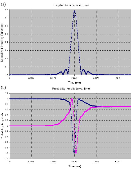
Using these parameters, we obtain at time at from the left edge of the TC, if is set to , and hence atom-cavity entanglement in Eq. (3). As atom B travels across the cavity, the time-dependent atom-cavity coupling parameter and the evolution of the probability amplitudes of states (blue) and (pink) in Eq. (3) are displayed in Fig. 2. In our calculations we neglect the insignificant effect of the mode tail on the probability amplitudes of the entangled state—less than beyond . Another even less significant source of error in our design is the coupling of the waveguides in the RC to the cavity13,14, which is simply circumvented by keeping in Fig. 1 sufficiently large (i.e., ).
Having entangled atom and the cavity, the second stage of the conditional teleportation protocol is to inject atom (whose trajectory is illustrated by the blue dashed line in Fig. 1), which is initially (i.e., at time ) in an arbitrary (or an unknown) quantum state,
| (5) |
Thus at time , the state of the whole system is written as
| (6) |
Once atom arrives at the detector, right before the detection, say at time , the state of the whole has evolved into
| (7) | |||||
which would reduce to Eq. (6) of Ref. (2), if were spatially uniform in Eq. (1).
In the derivation of Eq. (7), the contribution of in Eq. (1) is neglected, since atom is sufficiently far from the cavity when atom is injected. At times close to , although , neither atom alone nor combined can start the Rabi oscillation.7 On the other hand, as atom proceeds its coupling to the cavity mode increases, while the coupling of atom decreases. This means that the effect of becomes even less significant for times greater than .
The third stage of the conditional teleportation protocol is the measurement of the state of atom . If the result is , the combined state of atom and the cavity becomes
| (8) |
The denominator in Eq. (8) is simply the norm of the unnormalized state in the numerator. We obtain in Eq. (8) if we set , and thus
| (9) |
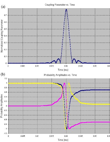
That is, the initial arbitrary (or unknown) state of atom has been teleported to atom , conditional on detecting atom in state , which occurs with probability . The time-dependent coupling parameter for atom and the evolution of the probability amplitudes of states (shown in pink), (shown in blue), and (shown in yellow) for the unnormalized state (i.e., the numerator) in Eq. (8) are shown in Fig. 3. Note that as time elapses Eq. (8) transforms into Eq. (9). Note also that atom arrives at at time (i.e., ). After an additional distance of , the fourth stage of our conditional teleportation and detection protocol begins as atom enters the RC at time (i.e., ). Next we study how to detect its state.
3 Readout Circuit
We can write the atom-maser Hamiltonian, under the dipole and rotating wave approximations, as15
| (10) |
where
| (11) |
is the Rabi frequency and is the frequency of the maser, whose polarization is also matched with the atomic dipole moment, , of the atom. In the following we will first assume a constant to simplify the explanation of the detection mechanism, and then we will modify the analysis to apply to our proposed PCQC, where is not constant.
Assume that atom in state [see Eq. (9)] enters a uniform field region at time and interacts during a time interval . Then its probability amplitudes at time can be computed to be16
| (12) |
| (13) |
where , , and are defined as follows.
| (14) |
| (15) |
| (16) |
After this interaction, atom interacts with a second uniform field region for the same time interval starting at time . The probability amplitudes, and , in this case can be also found from equations (12) and (13) by replacing , , and with , , and , respectively.
Note that one can also treat these two uniform field regions as a single uniform field region with an interaction time of . In this letter, however, we also intend to show that our RC has the potential to be an atomic interferometer, like a Ramsey interferometer.16 In order to hint how this could work, we design two separate oscillating field regions based on two parallel waveguides as discussed below. Implementation of a fully working interferometer, however, requires further consideration.
After atom has interacted with the two uniform field regions, we can implicitly write the final state of atom at time , before detection as
| (17) |
where is the probability amplitude of the atom being in state at time if it is initially prepared in state . For example if the atom is initially in state then it evolves into at time .
Having interacted with both waveguides, atom is finally detected by an ionization detector, as shown in Fig. 1. The probability of finding it in the excited state is
| (18) |
Superscripts and represent the real and imaginary part, respectively.
We can simplify Eq. (18) by writing Eq. (9) in the form
| (19) |
where we have implicitly set , , , and .
Then, at four different values we evaluate , , , and directly and measure . Thus having obtained four equations, we can find , , , and hence . Note that, although we have only two unknowns in Eq. (19), it is convenient to use four equations due to the form of Eq. (18). This demonstrates that one could detect the teleported state with our proposed device. In order to measure , we need an atomic beam of identically prepared single atoms, since multiple observations are necessary to estimate the probability. Since the TC only has a 25 percent conditional success rate, incoming atoms to the RC will not be identical. Thus if atom of the relevant pair is not detected in the excited state, the corresponding atom measurement is discarded from the calculation of .
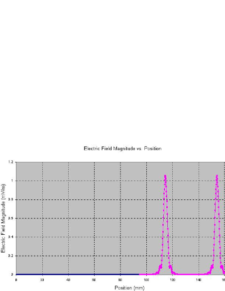
Finally, we describe how to apply these ideas to our proposed PCQC. Remember that atom in state enters the RC at time . The steady-state mode profiles of the waveguides are calculated by two-dimensional-finite-difference-time-domain (2D-FDTD) method with discretizations of and in the horizontal and vertical directions, respectively. We have designed the waveguides as coupled-cavity-waveguides17,18 to allow the atoms sufficiently large void regions through which to travel freely without a resonant-dipole-dipole-interaction or the Casimir-Polder effect (see Fig. 1). The steady-state cross section of the electric field magnitude, for , along the path of atom is shown in Fig. 4. At the steady state the coupling between the two parallel waveguides19-22 is not significant.
In our calculations we assume that atom interacts with two separate nonuniform waveguide modes of total width , shown by the pink curve in Fig. 4. In other words we truncated their tails (shown by blue in Fig. 4.), which overlap with the cavity mode. The effect of this truncation in our design is observed to be negligibly small. We have observed that the coupling of waveguide modes on the cavity mode is less than the cavity coupling to waveguides, which does not effect the probability amplitudes more than .
Since there is no feedback mechanism, as there is in the atom-cavity interaction, the atom-waveguide interaction can be described by a Markoff approximation. In other words, when an atom emits a photon into the waveguide, it leaves the interaction region immediately and cannot act back on the atom. Then the waveguides must be designed in such a way that total rate of spontaneous emission into the waveguide and the free-space lossy modes is sufficiently low as atom traverses them. In our design considering estimated effective transverse cross section of corresponding three-dimensional waveguide mode the maximum probability of spontaneous emission for a given atom is estimated to be on the order of .23 Thus, it is safe to assume that the Bloch vector of atom can be manipulated without being correlated with the defect mode24 of the waveguides.
The total interaction time with the parallel waveguides is also , as in uniform case above, with (i.e., ) for each. Note that, since the Rabi frequency, , is proportional to , the pink part of the curve in Fig. 4 also describes the position dependence of the Rabi frequency if multiplied by . Thus the evolution of the teleported state, as it interacts with the parallel waveguides, can be determined numerically by exploiting equations (12) and (13) successively, replaced with the maximum tolerated time-step, which is in our case (i.e. time for atom to travel ).
Thus, right before the detection, the final state is , which can be written exactly in the form of Eq. (17). The probability of detecting atom in the excited state is then given by Eq. (18), and following the same method as in the uniform case above, we can easily detect , the state output by TC.
As an example, assume that the final state of the TC [see Eq. (19)] is
| (20) |
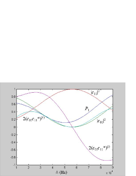
The corresponding calculated values of (green), (red), (light blue), (purple), and the value of (dark blue), which will be measured, are shown in Fig. 5. Picking four different values of , we can easily determine that and .
4 Discussions
Due to the electromagnetic scalability of photonic crystals one could also implement this device in more compact form in the optical regime. In this case, however, the electric field gradient and the momentum recoil of the atom would also have to be analyzed. In the microwave regime studied in this letter, the small momentum recoil due to a microwave photon does not cause external degrees of freedom (i.e., the position or momentum) of the atom to couple with its internal degrees of freedom (i.e., the ground or excited state).
To implement our PCQC, one should also engineer the surface states, which reside at the air-photonic crystal interfaces. These surface modes may also become correlated with the atoms exiting the crystal. These modes can be handled, however, by appropriate termination of the crystal.25-28
5 Conclusions
In conclusion, we have designed an integrated conditional teleportation circuit with readout in a single PC chip. Our proposed PCQC can be implemented by current or near future semiconductor processing technologies and experimental techniques. Even the detectors and sources illustrated in Fig. 1 could also be integrated—the feasibility of single atom detection on a PC chip has already been demonstrated29, as have PC based lasers.30,31 The RC part of our device can not only be used with the TC but also can be used independently, or integrated with other compatible optical circuits to read out atomic states. It also hints at the potential for implementation of atomic interferometers, such as the Ramsey interferometer, in photonic crystals.
Achieving good mode-matching stability becomes quite cumbersome for many multiply nested interferometers in optical quantum computing. Photonic crystals, however, may be an especially promising paradigm as robust quantum circuit boards for delicate, next generation, scalable optical quantum computing and networking technologies, as well as scalable quantum dynamic random access memory32, where qubits are refreshed using PC based cyclical quantum circuits. Integrated PC devices, such as planar waveguides and elementary interferometer modules, could replace the current bulky elements in linear optical quantum circuits. Furthermore, such devices could be made quite compact using PC integrated with single photon sources.33
Acknowledgments
This work was supported in part by the National Security Agency (NSA) and Advanced Research and Development Activity (ARDA) under Army Research Office (ARO) Grant No. DAAD19-01-1-0520, by the DARPA QuIST program under contract F49620-02-C-0010, and by the National Science Foundation (NSF) under grant ECS-0202087.
References
- [1] C. H. Bennett, G. Brassard, C. Crepeau, R. Jozsa, A. Peres, and W. K. Wootters, “Teleporting an unknown quantum state via dual classical and Einstein-Podolsky-Rosen channels,” Phys. Rev. Lett. 70, 1895–1899 (1993).
- [2] S.-B. Zheng, “Scheme for approximate conditional teleportation of an unknown atomic state without the Bell-state measurement,” Phys. Rev. A 69, 064302–064304 (2004).
- [3] M. A. Nielsen and I. L. Chuang, Quantum Computation and Quantum Information (Cambridge University, 2000).
- [4] E. S. Guerra, “Teleportation of atomic states via cavity quantum electrodynamics,” arXiv: quant-ph/0409194.
- [5] D. Bouwmeester, J.-W. Pan, K. Mattle, M. Eibl, H. Weinfurter, and A. Zeilinger, “Experimental quantum teleportation,” Nature (London) 390, 575–579 (1997).
- [6] M. L. Povinelli, S. G. Johnson, S. Fan, and J. D. Joannopoulos, “Emulation of two-dimensional photonic crystal defect modes in a photonic crystal with a three-dimensional photonic band gap,” Phys. Rev. B 64, 075313–075320 (2001).
- [7] D. Ö. Güney and D. A. Meyer, “Creation of entanglement and implementation of quantum logic gate operations using a three-dimensional photonic crystal single-mode cavity,” submitted to J. Opt. Soc. Am. B, arXiv: quant-ph/0603087.
- [8] Shi-Biao Zheng, Department of Electronic Science and Applied Physics, Fuzhou University, Fuzhou, 350002, China (personal communication, 2005).
- [9] S. Osnaghi, P. Bertet, A. Auffeves, P. Maioli, M. Brune, J. M. Raimond, and S. Haroche, “Coherent control of an atomic collision in a cavity,” Phys. Rev. Lett. 87, 037902–037905 (2001).
- [10] L. Davidovich, A. Maali, M. Brune, J. M. Raimond, and S. Haroche, “Quantum switches and nonlocal microwave fields,” Phys. Rev. Lett. 71, 2360–2363 (1993).
- [11] X. Maitre, E. Hagley, G. Nogues, C. Wunderlich, P. Goy, M. Brune, J. M. Raimond, and S. Haroche, “Quantum memory with a single photon in a cavity” Phys. Rev. Lett. 79, 769–772 (1997).
- [12] S. G. Johnson and J. D. Joannopoulos, “Block-iterative frequency-domain methods for Maxwell’s equations in planewave basis,” Opt. Express 8, 173–190 (2001).
- [13] S. Fan, “Sharp asymmetric line shapes in side-coupled waveguide-cavity systems,” Appl. Phys. Lett. 80, 908–910 (2002).
- [14] E. Waks and J. Vuckovic, “Coupled mode theory for photonic crystal cavity-waveguide interaction,” arXiv: physics/0504077.
- [15] M. O. Scully and M. S. Zubairy, Quantum Optics (Cambridge University, 1997).
- [16] N. Ramsey, Molecular Beams (Clarendon, Oxford, 1956).
- [17] A. Martinez, A. Garcia, P. Sanchis, and J.Marti, “Group velocity dispersion model of coupled-cavity waveguides in photonic crystals,” J. Opt. Soc. Am. A 20, 147–150 (2003).
- [18] M. Loncar, T. Doll, J. Vuckovic, and A. Scherer, “Design and fabrication of silicon photonic crystal optical waveguides,” J. Lightwave Technol. 18, 1402–1411 (2000).
- [19] S. Boscolo, M. Midrio, and C. G. Someda, “Coupling and decoupling of electromagnetic waves in parallel 2-D photonic crystal waveguides,” IEEE J. Quantum Electron. 38, 47–53 (2002).
- [20] S. Kuchinsky, V. Y. Golyatin, A. Y. Kutikov, T. R. Pearsall, and D. Nedelikovic, “Coupling between photonic crystal waveguides,” IEEE J. Quantum Electron. 38, 1349–1352 (2002).
- [21] T. Koponen, Tunnelling of Light in Photonic Crystal Waveguides (Thesis, University of Jyv skyl , Finland, 2003).
- [22] C. J. M. Smith, R. M. De La Rue, M. Rattier, S. Olivier, H. Benisty, C. Weisbuch, T. F. Krauss, R. Houdre, and U. Oesterle, “Coupled guide and cavity in a two-dimensional photonic crystal,” Appl. Phys. Lett. 78, 1487–1489 (2001).
- [23] P. Domokos, P. Horak, and H. Ritsch, “Quantum description of light pulse scattering on a single atom in waveguides,” arXiv: quant-ph/0202005.
- [24] N. Vats, T. Rudolph, and S. John, “Quantum information processing in localized modes of light within a photonic band-gap material,” arXiv: quant-ph/9910046.
- [25] R. D. Meade, K. D. Brommer, A. M. Rappe, and J. D. Joannopoulos, “Electromagnetic Bloch waves at the surface of a photonic crystal,” Phys. Rev. B 44, 10961–10964 (1991).
- [26] F. Ramos-Mendieta and P. Halevi, “Surface electromagnetic waves in two-dimensional photonic crystals: effect of the position of the surface plane,” Phys. Rev. B 59, 15112–15120 (1999).
- [27] Y. A. Vlasov, N. Moll, and S. J. McNab, “Observation of surface states in a truncated photonic crystal slab,” Opt. Lett. 29, 2175–2177 (2004).
- [28] T. Ochiai and J. Sanchez-Dehesa, “Superprism effect in opal-based photonic crystals,” Phys. Rev. B 64, 245113–245119 (2001).
- [29] B. Lev, K. Srinivasan, P. Barclay, O. Painter, and H. Mabuchi, “Feasibility of detecting single atoms using photonic bandgap cavities,” arXiv: quant-ph/0402093.
- [30] A. Sugitatsu, T. Asano, and S. Noda, “Line-defect-waveguide laser integrated with a point defect in a two-dimensional photonic crystal slab,” Appl. Phys. Lett. 86, 171106–171108 (2005).
- [31] X. Checoury, P. Boucaud, J. - M. Lourtioz, O. Gauthier-Lafaye, S. Bonnefont, D. Mulin, J. Valentin, F. Lozes-Dupuy, F. Pommereau, C. Cuisin, E. Derouin, O. Drisse, L. Legouezigou, F. Lelarge, F. Poingt, and G. H. Duan, “ room-temperature emission of square-lattice photonic-crystal waveguide lasers with a single line defect,” Appl. Phys. Lett. 86, 151111–151113 (2005).
- [32] S. Bandyopadhyay, “Prospects for a quantum dynamic random access memory (Q-DRAM),” arXiv: quant-ph/0101058.
- [33] P. Kwiat and G. Milburn, “Optical approaches to quantum information processing and quantum computing,” in A Quantum Information Science and Technology Roadmap, 2004, http://qist.lanl.gov.
List of Figure Captions
Fig. 1. Illustration of the proposed photonic crystal quantum circuit. This illustration is not to scale.
Fig. 2. (a) The time-dependent atom-cavity coupling parameter and (b) the evolution of the probability amplitudes of states (blue) and (pink) in Eq. (3), as atom travels across the cavity.
Fig. 3. (a) Time-dependent coupling parameter for atom and (b) the evolution of the probability amplitudes of states (pink), (blue), and (yellow) for the unnormalized state (i.e., numerator) in Eq. (8).
Fig. 4. The steady-state cross section of the electric field magnitude, for , along the path of atom (see text).
Fig. 5. Calculated values of (green), (red), (light blue), (purple), and to be measured value of (dark blue) (see text).