Theoretical analysis of the implementation of a quantum phase gate
with neutral atoms on atom chips
Abstract
We present a detailed, realistic analysis of the implementation of a proposal for a quantum phase gate based on atomic vibrational states, specializing it to neutral rubidium atoms on atom chips. We show how to create a double–well potential with static currents on the atom chips, using for all relevant parameters values that are achieved with present technology. The potential barrier between the two wells can be modified by varying the currents in order to realize a quantum phase gate for qubit states encoded in the atomic external degree of freedom. The gate performance is analyzed through numerical simulations; the operation time is ms with a performance fidelity above %. For storage of the state between the operations the qubit state can be transferred efficiently via Raman transitions to two hyperfine states, where its decoherence is strongly inhibited. In addition we discuss the limits imposed by the proximity of the surface to the gate fidelity.
I Introduction
The idea of encoding information in quantum two–level systems (qubits) instead of in classical bits promises a revolution in the way we process and communicate information niel . Quantum computers, i.e., processing units manipulating qubits instead of classical bits, would lead to an intrinsic speed-up of calculation that is not possible with a classical computer shor ; grov . For this purpose, a set of controlled operations is necessary, that substitute the network of electronic logic gates of present microelectronics. Analog to classical bits, also for qubits a limited set of universal gates exists that allows to implement networks for the execution of any quantum algorithm gate . Such universal gates operate on single qubits and on pairs of qubits. Whereas the design of single–qubit operations is conceptually simple and experimental implementations are within the reach of current technology in many cases, two–qubit operations are more demanding in terms of both theoretical and experimental investigations.
Several schemes for the realization of two–qubit gates with atoms or ions have been proposed in the last years cira ; turc ; cala ; jaks ; bren ; char and a considerable amount of progress has been recently realized for the future implementation of quantum information with cold atoms in optical lattices mande ; porto . Many of these schemes have been elaborated for ideal systems (harmonic oscillators, two–level systems, etc.) or under simplifying approximations for the sake of simplicity, in order to illustrate the idea on which the gate is based. The realization of such schemes in an experimental setup, where the characteristics of the real physical system are inevitably to be taken into account, is often a formidable task. The inclusion of realistic features and values requires a reexamination and modification of the schemes presented in the literature, in order to exploit all properties of the real physical system. For instance, the collisional gate with switching potentials proposed in cala exploits the complete revivals of wave packets in harmonic traps, which are difficult to achieve for neutral atoms, and deviations from harmonicity pose limiting restrictions to the performance of the gate negr . More realistic proposals for quantum gates are thus required.
With the spirit just outlined, we reconsider the two–qubit gate initially proposed in Ref. char . Two atoms are trapped in a double well potential. The ground () and first excited () vibrational states of each well are used as qubit logic states and the phase gate operation occurs via selective interaction between the atoms in the classically forbidden region under the potential barrier that separates the two atoms. In this paper we investigate the feasibility of such a scheme with neutral atoms on atom chips. Instead of assuming ideal trapping potentials for the atoms to facilitate numerical analysis, we derive here the exact potential created by appropriate stationary and time-dependent currents and bias magnetic fields on atom chips. The finite size of the current–carrying wires is also taken into account and realistic values for all physical parameters are used. In addition we consider also effects of the proximity of the surface, like spin flips and decoherence. Moreover, we specialize our discussion to neutral Rb atoms. In this way our investigations are much closer to the experimental conditions and our results show how the implementation of such a scheme is indeed feasible.
In spite of the improved realism of our investigations, some features of the real system are neglected in our analysis. Nonetheless, we expect that their role is marginal and/or can be minimized. Van deer Waals and Casimir forces between the atoms and the chip surface are not taken into account, since these effects become negligible when the atoms are kept sufficiently distant from the chip surface. Similarly, fabrication defects, such as roughness of the chip surface and imperfections in the atom chip are not taken into account, since they were shown to be sufficiently small, and the potentials sufficiently smooth kruger05 when using the appropriate fabrication techniques Gro04 . Thermal fluctuations of currents in the metal layers of the atom chip are another important issue Henkel ; Rekdal04 ; Varpula84 They may lead to loss of the atoms, and to decoherence of quantum states. However, we shall show that one can transfer the qubit state from the external degree of freedom to the internal one, using two clock states whose decoherence is strongly reduced harb ; treu and the important aspect to consider is the atom loss. Therefore, in spite of these approximations, our analysis is a significant step towards the first implementation of a phase gate with neutral atoms on atom chips.
The outline of the paper is as follows: in Sec. II we discuss the properties of Rb atoms that are relevant for our analysis and describe the architecture of wires and bias magnetic fields on atom chips that create a double–well potential for the two atoms with strong confinement in one dimension. We also give the values of currents, bias fields, and wire sizes that realize this trap. In Sec. III we give the results of our numerical investigations on the performance of the phase gate. We show that high fidelity () can be achieved with short operation times ( ms). In Sec. IV we show how to transfer the qubit state from the external degree of freedom to two hyperfine (magnetic tappable clock) states with Raman transitions. The relative phase of the two hyperfine states is insensitive, to first order, to fluctuations of the magnetic fields, thus, preserving the purity of the qubit state for long time. Finally in Sec. V we relate the achievable gate operation times to the expected atomic life times and coherence time, to estimate a realistic fidelity. Whereas the decoherence can be avoided by storing the qubits in the clock states, the loss of qubits due to thermally induced spin flips remains, and limits the fidelity of operations. The Appendix contains details concerning the magnetic field created by the currents on the atom chip.
II Double-well potentials with magnetic fields on atom chips
Atom chips are versatile integrated microstructures for the manipulation of samples of atoms in the ultracold and quantum degenerate regime (see Ref. folm and references therein). Trapping potentials for neutral atoms can be created near the chip surface. We shall consider the simple case of homogeneous bias magnetic fields and magnetic fields created by dc (but time–dependent) currents. The spin of slow, cold atoms remains adiabatically aligned with the magnetic field. The trapping magnetic potential, in the weak field approximation, is expressed by
| (1) |
where is the Bohr magneton, is the Landé factor, is the azimuthal quantum number, and is the magnetic field. In section III, a higher order accurate formula – derived from the Breit-Rabi approach breit – will be used in the numerical simulations, but we limit our discussion to the first order term given in Eq. (1) for the sake of simplicity.
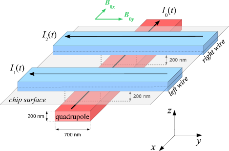
The most simple configuration of wires and bias magnetic fields that creates a double–well potential is shown in Fig. 1 homm . A longitudinal wire along (hereafter, quadrupole wire) carrying a dc current and a uniform bias magnetic field perpendicular to the wire create a quadrupole potential, with a zero magnetic field along a line parallel to the quadrupole wire. Clearly, along this line the magnetic field is minimum, but Maiorana spin flips occur at zero magnetic field, which result in atom losses. Therefore the minimum is shifted to a non–zero value with the addition of a second uniform bias magnetic field , orthogonal to the first one and parallel to the chip surface. Two more wires (hereafter, left and right wire, respectively), perpendicular to the quadrupole wire, carry a dc current , whose magnetic fields give rise to a modulation of the trapping potential.
In consideration of the small extension of the system (a few microns), the assumption of infinitely thin wires is too crude an approximation. Therefore in the potential (1) we shall use the expression of the magnetic field created by currents flowing through wires with finite rectangular sections (a typical shape of wires on atom chips). Details of the calculation are given in the Appendix.
A trapping potential with two well-separated minima, as shown in Figure 2(a), is created with the values mA, , G, and G. The three wires have an identical rectangular section, of width nm and height nm, and the centers of the left and right wires are m apart. The center of the quadrupole wire is at a distance nm under the chip surface, whereas the left and right wires lie on the chip. We stress that the values for the required transversal confinement has been approached even in the first experiments with nano fabricated atom chips fol00 ; folm and the currents, bias fields, size and distances of the wires are within current laboratory conditions notedens .
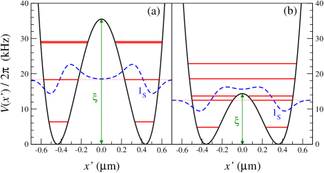
The two potential minima are at a distance of 1.19 m from the surface, and the line joining them is slightly tilted by an angle from the axis. This angle defines the new axis along which the dynamics will take place (see ciro for details). We also define a new axis parallel to the chip surface and perpendicular to . The axis remains unchanged. Since the trapping frequencies at the two minima verify the condition notefreq , transverse vibrations do not get excited during the gate operation (provided that the energy of the atoms is less than the quanta of transverse vibrations), and the trapped atoms will experience a quasi one–dimensional (1D) dynamics.
The value of the magnetic field at the two minima is G. This value minimizes the decoherence induced by fluctuations of the dc currents for the hyperfine states and of the ground state of Rb treu . These clock states will be used to store the qubit information at the end of the gate operation, as described in Sec. IV.
III Gate operation
Compared to previous static proposals ciro , we implement here a time-dependent phase gate in a spirit similar to the one of Ref. char .
As it can be noticed in Figure 2(a), when the barrier is high the translational wavefunctions of the atoms do not overlap in the inter–well region. In this type of environment, the atoms do not interact. On the other hand, when the barrier is lowered, as in Figure 2(b), tunneling takes place and the probability of finding the atoms in the classically forbidden region is not negligible any more. As a consequence, the energy splitting between the symmetric and anti–symmetric state combinations increases quickly when the barrier height is lowered. This effect is clearly state-selective in the sense that it affects differently the ground and excited translational states. It therefore constitutes an interesting candidate for the implementation of a conditional logical gate.
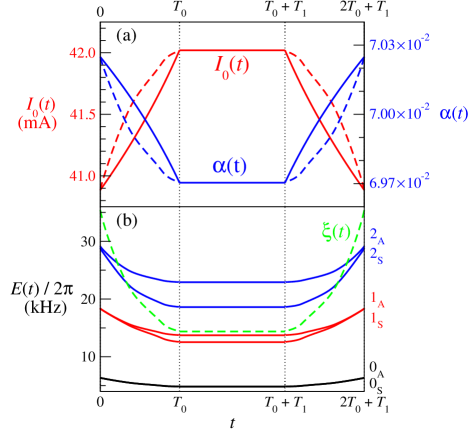
In the present scheme, the barrier height is controlled by varying simultaneously the intensities and in the quadrupole and in the perpendicular wires. In a first and simple implementation of the phase gate, we impose a linear variation of the barrier height with time. The phase gate is decomposed in three steps:
- •
-
•
When the inter–well barrier is fixed at its lowest value, such that a large inter–atomic interaction takes place.
-
•
Finally, when the inter–well barrier is raised again until the initial condition is recovered.
The linear variation of is obtained by changing and only, as depicted by the solid lines shown in Figure 3(a). We have verified that this simultaneous variation of the dc currents does not modify the direction along which the dynamics is taking place. In addition, the value of the magnetic field at the potential minima remains equal to 3.23 G during the whole gate operation. The dynamics is therefore quasi–adiabatic if s (hereafter we write instead of ).
The gate operation is followed by solving the time–dependent Schrödinger equation along the double-well direction for the wave packet describing the motion of the two atoms
| (2) |
The two–dimensional time–dependent Hamiltonian is written as
| (3) |
where denotes the kinetic energy operator along the –coordinate. The two–dimensional potential is given by the following sum
| (4) | |||||
where is the trapping potential (1) created by the atom chip and represents the averaged interaction potential between the two atoms at time
| (5) |
This last expression is obtained by averaging the three–dimensional delta function interaction potential over the lowest trap states along the and directions cala . One can note that the atom–atom interaction strength is proportional to the s–wave scattering length . Since the orthogonal trapping frequencies and vary slightly during the gate operation notefreq , the averaged interaction strength is also slightly time-dependent.
We solve the time-dependent Schrödinger equation (2) in a basis set approach by propagating the initial state of the two–atom system in time. We start with the atoms initially in one of the first four eigenstates , , , or of the double–well potential (4). The wavefunction is then expanded as
| (6) |
where represent the wavefunctions associated to the instantaneous eigenstates of the two–dimensional potential of Eq. (4). Inserting this expansion into the time–dependent Schrödinger equation (2) yields the following set of first order coupled ordinary differential equations for the complex coefficients
| (7) |
where denotes the energy of the eigenstate and is a time–dependent non–adiabatic coupling arising from the time variation of the barrier height
| (8) |
This set of equations is solved using an accurate Shampine–Gordon algorithm shamp . For each value of the duration we adapt in order to obtain an accurate conditional phase gate, with .
At the end of the propagation () the coefficients are analyzed to calculate the infidelity of the gate
| (9) |
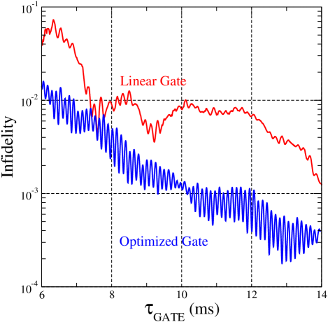
where the sum runs over all possible initial qubit states. The infidelity is therefore a measure of the deviation from adiabaticity which arises from the non-adiabatic couplings . This quantity is plotted in Figure 4 (red line for the linear gate) as a function of the gate duration. It shows an oscillatory behavior partially similar to the one observed with atoms trapped in an optical lattice char . The succession of maxima and minima is a signature of constructive and destructive interferences between two distinct pathways of excitation of the initial qubit state. Indeed the initial state may be excited in the time intervals and , when the barrier is lowered and raised. The nature of this interference depends on the phases which develop during the gate operation char . The periodicity of the oscillation is simply related to the Bohr frequencies associated with the energy splitting of the two–atom eigenstates. The linear gate configuration proposed here can achieve a relatively high fidelity of about 99.6% in just 7.6 ms.
One should also realize that in the general case the couplings between the initial qubit states and the other accessible two–atom eigenstates vary with time. These couplings effectively increase when the inter–well barrier approaches the energy of the initial state. The linear gate proposed until now is therefore far from being optimal for the maximization of the gate fidelity.
We have thus implemented an optimized gate which tends to minimize these couplings during the whole gate duration. For this purpose, we impose a fast variation of the barrier height at early times , whereas this variation is much slower when . This is done by choosing
| (10) |
In this expression, is a dimensionless proportionality factor, which can be decreased to achieve larger gate durations. The first derivative with respect to time of the barrier height is therefore chosen such that the maximum effective first–order coupling between the highest energy qubit state and all other states remains constant during the whole gate duration. With this approach, higher fidelities are expected when compared to a linear gate of the same duration.
The variations of and for this optimized gate are shown as dashed lines in Figure 3(a). Figure 4 shows that the optimized gate infidelity (blue line) is, on average, improved by a factor 6 when compared to the linear gate. As a consequence, this optimized gate can achieve fidelities of 99% in 6.3 ms and of 99.9% in 10.3 ms.
IV Using both degrees of freedom as qubit states
When neutral atoms are used, it is possible to employ either the vibrational or the internal states as qubit states. Section III has shown that vibrational states are very promising in terms of gate performance. However, the readout of the qubit after the gate operation seems to be a difficult task in comparison to the readout of internal states, for which observation of fluorescence emitted from selected transitions is a well established technique. Moreover, a closer examination of the hyperfine structure of the ground state of Rb provides further motivation for the use of internal states.
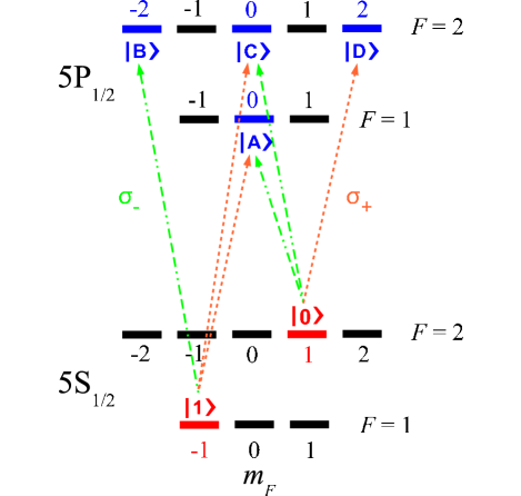
The hyperfine structure of the ground state of Rb is shown in Figure 5: eight sublevels have to be considered, three with and five with . Only three of these eight sublevels (the states , , and ) are low–field seeking states which can be trapped by static magnetic potentials folm . In addition, the two hyperfine levels and have opposite Landé factors. As a consequence, they experience identical magnetic potentials. A more precise estimation that goes beyond the linear approximation given in Eq. (1) shows that the difference of the Zeeman shifts experienced by these two states is minimum at G harb . At this field the states and are insensitive to field fluctuations at first order. The decoherence of an arbitrary superposition of the two states and due to fluctuations in the current intensities (which entail fluctuations in the magnetic field and thus in the potential (1)) is thus strongly inhibited. Indeed, coherent oscillations between the states and have recently been observed and the decoherence time has been estimated to be s s treu . The inhibition of decoherence is a fundamental issue in quantum computation, since the coherence of the quantum state is an essential ingredient. It would thus be desirable to use the clock states and for the storage of quantum information.
In fact, we can use both degrees of freedom as qubits: when information must be processed, it will be encoded in the external degree of freedom and the gate operation will be done as described in the previous Section. At the end of the gate operation, the qubit state can be transferred to the internal degree of freedom and stored there until new operations are performed or until the final readout. In order to realize this transfer from one degree of freedom to the other, we need to swap the states associated with these two degrees of freedom, according to
| (11) |
In this way, an arbitrary qubit state encoded in the vibrational states as
| (12) |
is transformed into
| (13) |
and vice versa. Eq. (12) assumes that the internal degree of freedom of the two atoms has been initialized to the state . The map given in Eq. (11) is a selective switch from the internal state ( respectively ) to the state ( respectively ) under the control of the vibrational state. In order to realize it, we propose the use of two–photon Raman transitions.
The realization of such a two–photon Raman transition via intermediate states requires a careful analysis stec . The and levels have eight hyperfine states with or 2, whereas the level comprise sixteen states with , 1, 2 or 3. The Raman transition requires two lasers, one with polarization (frequency and wave vector ), the other with polarization (frequency and wave vector ). When the laser frequencies and are kept below the transition, the states in can be neglected, being detuned by about 7 THz. From now on we therefore restrict our analysis to the states and , and to the following states
Taking into account all possible transitions according to the selection rules imposed by the polarizations, the Hamiltonian in the usual rotating–wave approximation is
| (14) |
with
where we have defined the phases
and where and are the Rabi frequencies associated with the interaction between the electric dipole of the atom and the electric field of the lasers. is the atomic position operator, and h.c. denotes the Hermitian conjugate.
From the Hamiltonian (14) one can derive the Heisenberg equations of motion for the operators , with , 1, A, , D. For instance, for the operator we get
| (15) | |||||
where
With the introduction of the “slow” variables
equation (15) becomes
When the lasers are strongly detuned from the atomic transition frequencies, one can obtain an effective Hamiltonian by imposing the adiabaticity condition eber ; wang . In this case, we get
where we have defined the detuning
| (16) |
Performing similar calculations for the operators , , , and after substituting them into and and including the diagonal terms into , we get the effective interaction Hamiltonians
| (17) |
and
| (18) |
where the phase is simply given by the difference
| (19) |
and the detunings are defined just as (16) by
When the initial atomic state is a superposition of and , as in our case, we can retain the terms containing and only, such that the effective interaction Hamiltonian reduces to
| (20) |
where {subequations}
| (21) | |||||
| (22) |
The presence of two states with (the and states) could seem problematic. When the lasers are very far detuned from resonance, the detunings from these two levels are almost equal: and . A destructive interference between these two quantum paths suppresses the Raman transition between the states and (see Eqs. (20)). In order to stimulate this Raman transition, the detunings from levels and must be significantly different. This condition can be realized in Rb , where the states and are separated by MHz and the natural line width of the level is about MHz. Finally, we comment the realization of the sideband excitation required by the transformation (11). It requires a laser linewidth much smaller than the vibrational angular frequency, i.e., much smaller than 10 KHz, a condition that can be reached experimentally with standard techniques ciro . It is also possible to produce pulses with specific shapes that optimize the transition probability and stimulate the transition in very short periods, so that the gate operation time is not significantly altered.
V Loss and decoherence
An important mechanism we have to consider in a realistic evaluation of the performance of quantum gates, is the possibility of loss and decoherence of the qubits during the operation. Especially in atom chips this is an important issue, since the cold atoms are perturbed by thermal electromagnetic fields generated by the nearby, hot solid substrate. This leads to heating, trap loss and decoherence Henkel ; Rekdal04 ; Varpula84 . Since the thermal induced couplings lead to similar timescales for all these undesired processes we consider the loss, which was studied in largest detail theoretical and experimentally ThLossExp . In addition, as we have seen in the previous section, the decoherence can be dramatically reduced by transferring the qubits o clock states during idle periods.
Following the treatment of Henkel one can estimate the atomic lifetimes for a setup like shown in Fig. 1. Assuming gold wires we find a typical lifetime of 0.8 s due to thermally induced spin flips and consequent loss of the qubit state. The left and right wires, which are closest to the atoms and carry small currents, give the largest contribution to the loss. In this configuration the best fidelity of is obtained for a gate operation time of ms.
Small changes in the trapping geometry can improve the fidelity: Since a big part of the loss comes from the left and right wires, one can fabricate them much thinner. Reducing the thickness of the double well wires to 50 nm would increase the lifetime to over 2 sec and increase the fidelity to 99.5 % at a gate operation time of 10 ms. This can be even more improved by a little bit different wire geometry for the quadrupole wire. A wider but thinner quadrupole wire (), and smaller left and right wires () will lead to lifetimes in excess of 3 s and consequently a better gate fidelity in the order of 99.7 % at a gate operation time of 11 ms.
Further improvements can be expected when optimizing the wire geometries. Two aspects have to be taken into account.
- •
-
•
A second consideration is using different materials, and cooling the chip surface, as investigated theoretically by Dikov05 . This should lead to even further improvements.
-
•
Directly fabricating the wires into semiconductor chips will give even better thermal coupling and allow the use of high resistivity materials for the wires, which should improve even further the gate performance.
Overall we conclude that for optimized geometries fidelities better than 99.9% should be possible in realistic settings with present day atom chip technology.
VI Summary and conclusions
We have presented a detailed analysis of the implementation of a quantum phase gate with neutral rubidium atoms on atom chips. Our analysis is quite close to the experimental conditions and is within the reach of current technology. We have shown how to create a double well potential near the surface of an atom chip and studied the performance of a phase gate, using as qubit states the vibrational states of two rubidium atoms, each sitting in one of the two wells. The gate operation is realized through an adiabatic modification of the potential barrier that separates the two wells. This implementation allows selective interaction between the vibrational states of the two atoms. We have found that, neglecting losses due to spin flips, a fidelity of 99.9% can be achieved in just 10.3 ms. We have also shown that the motional qubit state can be transferred to two hyperfine states with reduced decoherence. The estimation of loss due to thermally induced spin flips reduces slightly the gate fidelity, and improvements to reduce these effects have been discussed.
The results presented here are a significative improvement when compared to an implementation using a static trap ciro . For a fidelity above 99% the operation time is diminished from about 16.2 ms to 6.3 ms. The operation time could be further reduced using non-adiabatic changes of the barrier, as recent studies employing optimal control theory indicate vage , but the excitation of the perpendicular degrees of freedom might then become an issue.
VII Acknowledgments
M. A. Cirone, A. Negretti, T. Calarco and J. Schmiedmayer acknowledge financial support from the European Union, contract number IST-2001-38863 (ACQP). T. Calarco also acknowledges financial support from the European Union through the FP6-FET Integrated Project CT-015714 (SCALA) and a EU Marie Curie Outgoing International Fellowship, and from the National Science Foundation through a grant for the Institute for Theoretical Atomic, Molecular and Optical Physics at Harvard University and Smithsonian Astrophysical Observatory. The IDRIS-CNRS supercomputer center supported this study by providing computational time under project number 08/051848. This work has been done with the financial support of the LRC of the CEA, under contract number DSM 05–33. Laboratoire de Photophysique Moléculaire is associated to Université Paris-Sud. We wish to thank P. Krüger, J. Reichel and P. Treutlein for useful discussions about experimental details.
VIII Appendix
The magnetic field created by an infinitely thin and infinitely long straight wire is
| (23) |
where is the dc current flowing through the wire, is the distance to the wire and ( is the magnetic permeability of the vacuum). In the case of a wire of finite rectangular section, we average the magnetic fields created by many infinitely thin wires lying inside the finite section. For instance, for a dc current flowing in the positive direction through a wire with section (, ), the magnetic field components are
| (24) |
and
| (25) |
In Eq. (24) the integration over gives the –component
| (26) |
where . A final integration over gives
| (27) | |||||
After defining , analogous calculations for the component give
| (28) | |||||
References
- (1) M. A. Nielsen and I. L. Chuang, Quantum Computation and Quantum Information, Cambridge University Press, Cambridge (2000).
- (2) P. W. Shor, Proc. 35th Annual Symposium on Foundations of Computer Science (Shafi Goldwasser, ed.), IEEE Computer Society Press (1994).
- (3) L. K. Grover, Phys. Rev. Lett. 79, 325 (1997).
- (4) A. Barenco, C. H. Bennett, R. Cleve, D. P. DiVincenzo, N. Margolus, P. Shor, T. Sleator, J. A. Smolin, and H. Weinfurter Phys. Rev. A 52, 3457 (1995).
- (5) J. I. Cirac and P. Zoller, Phys. Rev. Lett. 74, 4091 (1995).
- (6) Q. A. Turchette, C. S. Wood, B. E. King, C. J. Myatt, D. Leibfried, W. M. Itano, C. Monroe, and D. J. Wineland Phys. Rev. Lett. 81, 3631 (1998).
- (7) T. Calarco, E. A. Hinds, D. Jaksch, J. Schmiedmayer, J. I. Cirac, and P. Zoller Phys. Rev. A 61, 022304 (2000).
- (8) D. Jaksch, J. I. Cirac, P. Zoller, S. L. Rolston, R. Côté, and M. D. Lukin, Phys. Rev. Lett. 85, 2208 (2000).
- (9) G. K. Brennen, C. M. Caves, P. S. Jensen, and I. H. Deutsch, Phys. Rev. Lett. 82, 1060 (1999).
- (10) E. Charron, E. Tiesinga, F. Mies, and C. Williams, Phys. Rev. Lett. 88, 077901 (2002).
- (11) O. Mandel, M. Greiner, A. Widera, T. Rom, T. W. Hänsch and I. Bloch, Nature 425, 937 (2003).
- (12) J. V. Porto, S. Rolston, B. Laburthe Tolra, C. J. Williams and W. D. Phillips, Phil. Trans. R. Soc. Lond. A 361, 1417 (2003).
- (13) A. Negretti, T. Calarco, M. A. Cirone, and A. Recati, Eur. Phys. J. D 32, 119 (2005).
- (14) P. Krüger, L.M. Andersson, S. Wildermuth, S. Hofferberth, E. Haller, S. Aigner, S. Groth, I. Bar-Joseph and J. Schmiedmayer, cond-mat/0504686.
- (15) S. Groth, P. Krüger, S. Wildermuth, R. Folman, T. Fernholz, D. Mahalu, I. Bar-Joseph, and J. Schmiedmayer, Appl. Phys. Lett. 85, 2980 (2004).
- (16) C. Henkel, M. Wilkens, Europhys. Lett. 47, 414 (1999); C. Henkel, S. Pötting, M. Wilkens, Appl. Phys. B 69, 379 (1999); C. Henkel, S. Pötting, Appl. Phys. B 72, 73 (2001); C. Henkel, Eur. Phys. J. D 35, 59 (2005);
- (17) P.K. Rekdal, S. Scheel, P.L. Knight, E.A. Hinds, Phys. Rev. A. 70, 013811 (2004); S. Scheel, P.K. Rekdal, P.L. Knight, E.A. Hinds, e-print arXiv:quant-ph/0501149.
- (18) T. Varpula, T. Poutanen, J. Appl. Phys. 55, 4015 (1984)
- (19) D. M. Harber, H. J. Lewandowski, J. M. McGuirk, and E. A. Cornell, Phys. Rev. A 66, 053616 (2002).
- (20) P. Treutlein, P. Hommelhoff, T. Steinmetz, T. W. Hänsch, and J. Reichel, Phys. Rev. Lett. 92, 203005 (2004).
- (21) R. Folman, P. Krüger, J. Schmiedmayer, J. Denschlag, and C. Henkel, Adv. At. Mol. Opt. Phys. 48, 263 (2002).
- (22) G. Breit and I. I. Rabi, Phys. Rev. 38, 2082 (1931).
- (23) J. Reichel, W. Hänsel, P. Hommelhoff, T. W. Hänsch, Appl. Phys. B 72, 81 (2001).
- (24) R. Folman, P. Krüger, D. Cassettari, B. Hessmo, T. Maier, and J. Schmiedmayer, Phys. Rev. Lett. 84, 4749 (2000).
- (25) By insulating the wires from the substrate by an evaporated layer as thin as 10 nm, relatively high current densities like that considered in our numerical simulations can be achieved Gro04 .
- (26) M. A. Cirone, A. Negretti, T. Calarco, P. Krüger, and J. Schmiedmayer, Eur. J. Phys. D 35, 165 (2005).
- (27) During the gate operation, the trapping frequencies vary in the ranges 13.0–10.9 kHz, 157.5–154.3 kHz and 153.8–150.9 kHz for , and respectivelly.
- (28) L. F. Shampine and M. Gordon, Computer solution of ordinary differential equations: the initial value problem, W. H. Freemann and Company, San Francisco, (1975). http://www.csit.fsu.edu/burkardt/f_src/ode/ode.f90
- (29) Most of the data on rubidium atoms used hereafter can be found in the notes by Steck at http://steck.us/alkalidata/
- (30) C. C. Gerry and J. H. Eberly, Phys. Rev. A 42, 6805 (1990).
- (31) L. Wang, R. R. Puri, and J. H. Eberly, Phys. Rev. A 46, 7192 (1992).
- (32) A.E. Leanhardt, Y. Shin, A.P. Chikkatur, D. Kielpinski, W. Ketterle, D.E. Pritchard, Phys. Rev. Lett. 90, 100404 (2003); M.P.A. Jones, C.J. Vale, D. Sahagun, B.V. Hall, E.A. Hinds, Phys.Rev. Lett. 91, 080401 (2003); D.M. Harber, J.M. McGuirck, J.M. Obrecht, E.A. Cornell, J. Low. Temp. Phys. 133, 229 (2003); Y. Lin, I. Teper, C. Chin, V. Vuleti c, Phys. Rev. Lett. 92, 050404 (2004)
- (33) B. Zhang, C. Henkel, E. Haller, S. Wildermuth, S. Hofferberth, P.Krüger, and J. Schmiedmayer Eur. Phys. J. D 35, 97 (2005) DOI: 10.1140/epjd/e2005-00227-1
- (34) V. Dikovsky, Y. Japha, C. Henkel, and R. Folman; Eur. Phys. J. D 35, 87 (2005) DOI: 10.1140/epjd/e2005-00203-9
- (35) D. Vager, B. Segev, and Y. B. Band, Phys. Rev. A 72, 022305 (2005).