Creation of Entanglement and Implementation of Quantum Logic Gate Operations Using a Three-Dimensional Photonic Crystal Single-Mode Cavity
Abstract
We solve the Jaynes-Cummings Hamiltonian with time-dependent coupling parameters under dipole and rotating-wave approximation for a three-dimensional (3D) photonic crystal (PC) single mode cavity with a sufficiently high quality (Q) factor. We then exploit the results to show how to create a maximally entangled state of two atoms, and how to implement several quantum logic gates: a dual-rail Hadamard gate, a dual-rail NOT gate, and a SWAP gate. The atoms in all of these operations are syncronized, which is not the case in previous studies [1,2] in PCs. Our method has the potential for extension to -atom entanglement, universal quantum logic operations, and the implementation of other useful, cavity QED based quantum information processing tasks.
1 Introduction
The superiority of quantum computing over classical computation for problems with solutions based on the quantum Fourier transform, as well as search and (quantum) simulation problems has attracted increasing attention over the last decade. Despite promising developments in theory, however, progress in physical realization of quantum circuits, algorithms, and communication systems to date has been extremely challenging. Major model physical systems include photons and nonlinear optical media, cavity QED devices, ion traps, and nuclear magnetic resonance (NMR) with molecules, quantum dots, superconducting gates, and spins in semiconductors [3].
In the last century, control over electrical properties of materials led to the transistor revolution in electronics. Now, in this century, PCs inspired great interest for controlling the flow of light. PCs are periodic arrays of dielectric materials, which would resemble the atomic structure of semiconductors if the dielectric materials were scaled down to atomic dimensions. If a defect is introduced by disturbing the periodicity of the crystal, a localized mode is allowed in that region. Similar to electronic band structure in semiconductors, acceptor or donor types of defect states can also be produced in a PBG, by locally removing or adding extra dielectric material, respectively. By tuning the parameters of the PC cavity, the frequency or the spatial profile of this localized state can be tailored on demand.
Known also as photonic band gap (PBG) materials, PCs seem to be especially promising as a base medium both for future laser based photonic integrated circuits and perhaps later on for advanced quantum network technologies as well [4-6]. Combining a high Q factor and an extremely small mode volume successfully in microcavities, PCs have already become an especially attractive paradigm for quantum information processing experiments in cavity QED [1,2,7].
Quantum logic gates and quantum entanglement constitute two building blocks, among others, of more sophisticated quantum circuits and communication protocols. The latter also allows us to test basic postulates of quantum mechanics.
In this work we propose an alternative method for creating entanglement and implementing certain quantum logic gates based on single mode PC microcavities. Our scheme requires high-quality PCs with Q-factor of around . Two-dimensional PC slabs, which have been demonstrated recently, have a Q-factor of only about -. Since today’s planar PC technology does not allow sufficiently high-Q cavities for our purposes, we must consider three-dimensional PCs despite the relative difficulty of their fabrication.
2 Theory
In this paper we first explore the possibility of mutually entangling two Rb atoms by exploiting their interaction, mediated by a single defect mode confined to a three-dimensional PC cavity. We then describe various logic gates that can be implemented using the same interaction. We achieve this in three steps: analysis of a single mode cavity (i) in a generic 3D PC, (ii) in a specific 2D PC and (iii) ultimately in a 3D version of the 2D PC of (ii). We assume that the defect frequency is resonant with the Rb atoms. Because the atoms are moving, the time-dependent Hamiltonian (Jaynes-Cummings Model) for this interaction in the dipole and rotating wave approximations is
| (1) |
where the summation is over two atoms, and , is the resonant frequency, is the -component of the Pauli spin operator and are atomic raising and lowering operators. and are photon destruction and construction operators, respectively. The time-dependent coupling parameters can be expressed as [1]
| (2) |
where is the peak atomic Rabi frequency over the defect mode and is the spatial profile of the defect state observed by the atom at time . is the angle between the atomic dipole moment vector, , for atom and mode polarization at the atom location.
We ignore the resonant dipole-dipole interaction (RDDI), because the atoms have their transition frequencies close to the center of a wide PBG and the distance between them is always sufficiently large that RDDI effect is not significant [2,8].
Initially we prepare one of the atoms, , in the excited state and the cavity is left in its vacuum state, so
| (3) |
The PC should be designed to allow the atoms to go through the defect. This can be achieved by injecting atoms through the void regions of a PC with a defect state of acceptor type. Since the spontaneous emission of a photon from the atoms is suppressed in the periodic region of the crystal, no significant interaction occurs outside the cavity. When the atoms enter the cavity, the interaction between the atoms is enhanced by the single mode cavity. This atom-photon-atom interaction allows us to design an entanglement process between atoms.
Given the initial state (3), the state of the system at time should be in the form
| (4) |
to satisfy the probability and energy conservation. We will show analytically that the amplitudes at time can be expressed in terms of the coupling parameters and the velocities of the atoms.
We can write the Schrödinger equation for the time-evolution operator in the form [9]
| (5) |
In the basis , the matrix elements of the Hamiltonian (1) are
| (6) |
| (7) |
| (8) |
Hamiltonian operator, , at different times commute, if is a multiple of by a factor of . This condition can be easily satisfied by the appropriate orientation of atomic dielectric moment of the incoming atoms with respect to electric field in equation (2). Then the formal solution to (5) becomes
| (9) |
where is defined as the integral of the Hamiltonian operator. By expanding the exponential (9) we obtain
| (10) |
Multiplying equation (10) by the initial state from the right and comparing with (4) gives
| (11) |
| (12) |
| (13) |
where we have defined
| (14) |
Recognizing the Taylor series for sine and cosine allows us to rewrite equations (11)-(13) as
| (15) |
| (16) |
| (17) |
For a single initially excited atom, , passing across the cavity we can set in equations (15)-(17), which gives the same result with equation (15) of [4]. The exact solution for the time-independent problem of identical two level atoms with a resonant single mode quantized field given in ref. [10] could be helpful to generalize our results to -atom case, see for example ref. [2].
Absent a rigorous calculation of the defect mode in the three-dimensional PC, let us just assume a generic spatial profile for the mode, which oscillates and decays exponentially. Thus, in (2) can be expressed as [1]
| (18) |
where , , , are the velocity of atom , the total path length of the atoms, defect radius, and the lattice constant of the PC, respectively.
We choose the velocity of atoms, , such that , a typical velocity range appropriate for both experiments and our calculations. This has two immediate advantages: First, we make Hamiltonians at different times commute, and thus greatly simplify the analytical analysis. Second, we syncronize the atoms, providing cyclical readout that could be synchronized with the cycle time of a quantum computer [24]. These conditions in previous studies [1,2] are not satisfied.
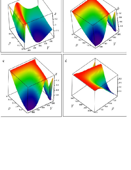
Using equations (15)-(18) we can express the asymptotic probability amplitudes, and , as functions of the and the . The results for and , when the initial state is , are displayed in Figures 1a and 1b, respectively. If the initial state is , corresponding probability amplitudes are illustrated in Figures 1c and 1d. Note that the surfaces in Figures 1b and 1c are the same. This is simply due to the symmetry in equation (16). To compute these surfaces we used the asymptotic (constant) values of the .
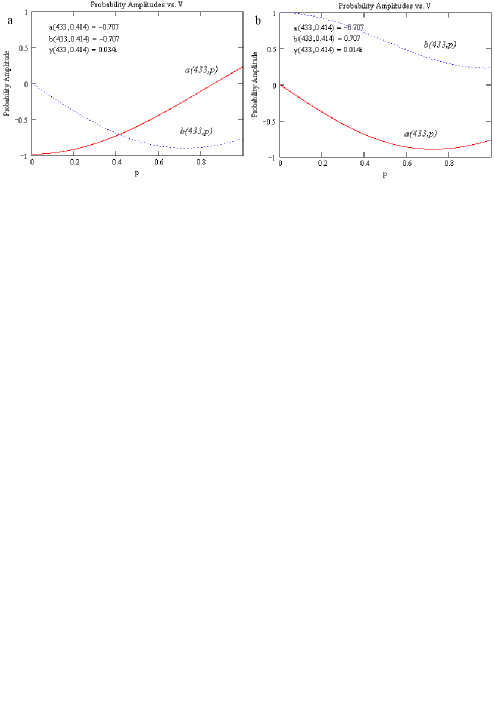
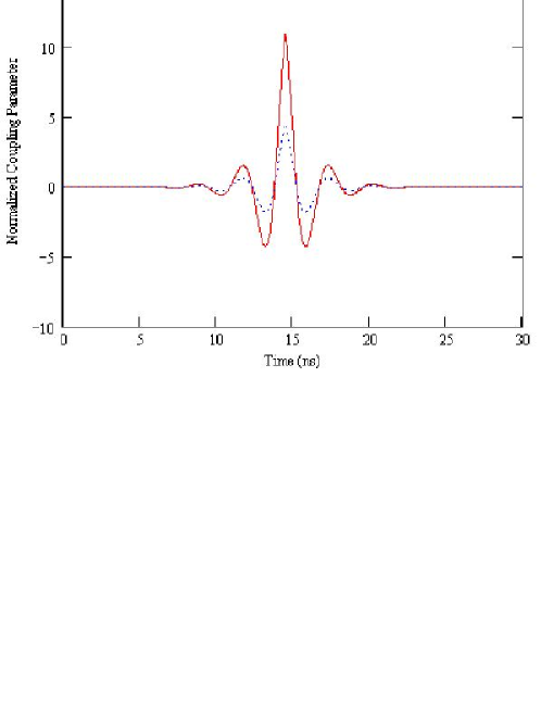
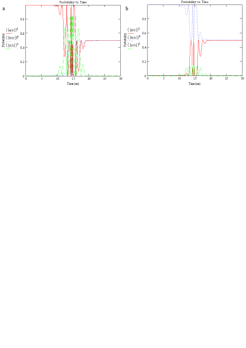
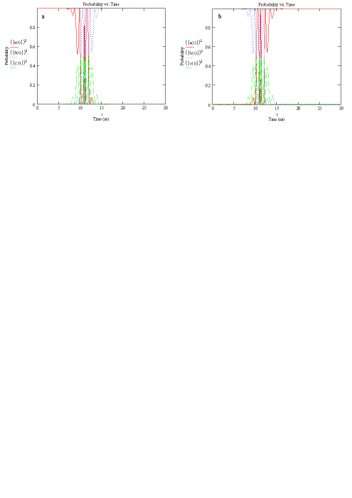
Fig. 2a illustrates a slice from the surface in Fig. 1a where the velocity of the atoms are, . Note that we obtain the maximally entangled state,
| (19) |
up to an overall phase, , when the velocities of the atoms, and the initial state is . Similarly if we keep the velocities of the atoms fixed but set the atom to be excited initially (i.e., ), we obtain the slice in Fig. 2b and thus the maximally entangled state,
| (20) |
up to the same overall phase factor as in equation (19). (In equations (19) and (20), and in the following, we omit the cavity state in the kets, since it factors out and does not contribute to logic operations with which we are concerned.)
The calculated coupling parameters in the reference frame of the atoms as a function of time, , with the specific values of , , , and are shown in Fig. 3. The solid red curve and blue dashed curve correspond to atom and , respectively. The total interaction time is less than .
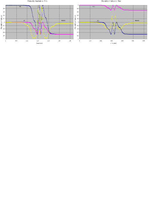
Probabilities , , and from equations (15)-(17) are graphed in Fig. 4. Fig. 4a shows the evolution of the probabilities when the initial state is . Note that the cavity is disentangled from the atoms and we end up with the final state (19). On the other hand if the initial state is , the time evolution of the probabilities is illustrated in Fig. 4b. Note that the final state in this setting becomes (20), since the cavity is again disentangled. From (19) and (20) it is clear that the quantum system we have described not only entangles the atoms but also operates as a dual-rail Hadamard gate [3] up to an overall phase.
Using the same quantum system one can also build a dual-rail NOT gate under certain conditions. If we set , for example, we obtain the following logical transformations, up to an unimportant global phase factor, which defines a dual-rail NOT gate (see fig. 5):
| (21) |
| (22) |
Furthermore using the Hamiltonian (1) it can be shown that initial state only gain a deterministic phase factor of in interaction picture. Once the conditions (21) and (22) are satisfied initial state is transformed into itself up to the same global phase with the states in (21) and (22). Thus, including these as possible initial states our dual-rail NOT gate also operates as a SWAP gate up to a relative phase of the state. During our analysis we have also observed that a dual-rail gate is also possible for some specifications.
3 Two-dimensional Photonic Crystal
In the preceding analysis we have assumed the generic form (18) for the spatial profile of the defect mode in order to demonstrate that, in principle, PC microcavities can be used as entanglers, and more specifically, as certain logic gates. In the following we apply these ideas to real two- and three-dimensional photonic crystal microcavity designs, to show that implementations of these quantum devices are indeed possible in these photonic systems. As the authors of [2] observe, however, “a rigorous calculation of the electromagnetic field in the presence of a defect in a 3D photonic crystal can be a difficult task”. In the following we address this task systematically.
First we consider a 2D photonic crystal design with a triangular lattice of dielectric rods with dielectric constant of (i.e., silicon) in Fig. 6. The radius of the rods is , where is the lattice constant. The symmetry is broken in the center by introducing a defect with reduced rod-radius of to form the microcavity of our quantum system. We assume that the atoms and travel along the dashed green lines shown in Fig. 6a, although any two of the obvious paths shown by dashed lines (or any void regions with line of sight of the cavity) work as well.
In order to find the probability amplitudes for the atoms as a function of time while travelling through the crystal, we need to calculate the coupling parameters in equation (14) and substitute them in equations (15)-(17). Once we obtain the probability amplitudes, we can demonstrate entanglement creation and construct logic gates as before. We also note that the quality factor of the cavity should be high enough that the interaction time (i.e., the logic operation time) is much less than the photon lifetime in the cavity. Below we show that typical logic operations take for the Hadamard gate and for the NOT or the SWAP gate. Thus a quality factor of should be sufficient for reliable gate operations. The quality factor of the cavity could be increased exponentially with additional period of rods in Fig. 6a [11]. We observe, however, that the spatial profile of the mode in Fig. 6b does not change significantly (and hence degrade the gate) after a certain number of periods. Thus, the exact number of periods required for a quality factor of is not essential to demonstrate our main goal in this paper, namely that such logic operations and entanglement creation are indeed possible in these photonic crystal structures.
In our generic profile (18), the coupling parameter is assumed to be real. However, for generality in real photonic crystals, we must allow it to be a complex parameter. Thus, the interaction part of the Hamiltonian (1) for a single-atom cavity interaction can be written as [12-15]
| (23) |
by incorporating complex coupling parameter into (1).
In a photonic crystal we can express the atom-field coupling parameter [12, 16] at the position of atom , as
| (24) |
where and are defined as
| (25) |
| (26) |
denotes the position in the dielectric where is maximum and is defined as the dielectric constant at that point. The cavity mode volume, , is given as
| (27) |
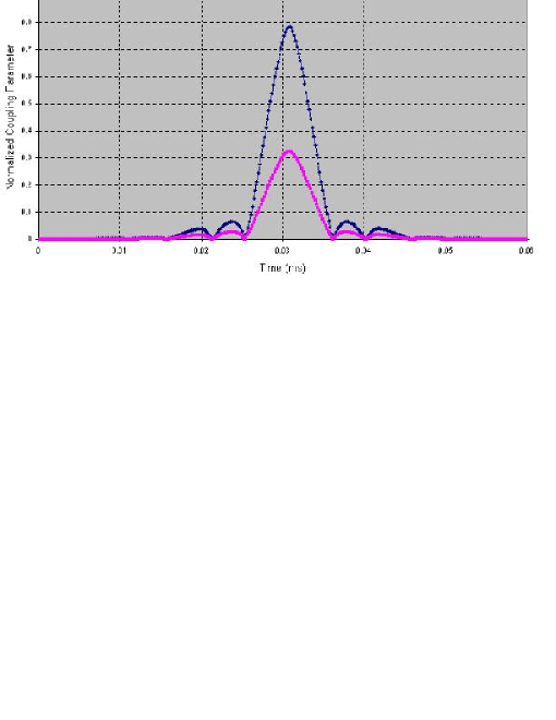
Using the block iterative plane-wave expansion method [17] we found the normalized frequency of the cavity mode shown in Fig. 6b to be . By setting , we tune the resonant wavelength to . At this wavelength, for the Rb atom is [1]. Since we observe that the energy density is concentrated in the center of the cavity, in equations (25) and (27) becomes . On the other hand, in equation (24) can be safely assumed constant for each atom, because our cavity mode is transverse-magnetic (TM) mode and its electric field polarization direction can always be assumed to have a constant angle with the atomic dipole moment vector, . We determined the coupling parameters as functions of time in the reference frame of moving atoms, as shown in Fig. 7. The tails of the coupling parameter functions do not contribute significantly to results due to exponential decay away from the cavity.
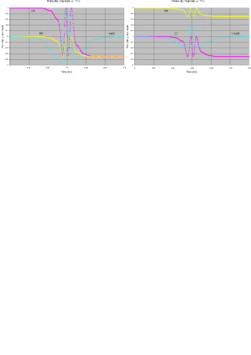
With these settings Fig. 8 demonstrates an entangler which operates as a dual-rail Hadamard gate. If the initial state is (i.e., atom is excited), we end up with state [see equation (19) and Fig. 8a]. If atom is initially excited (i.e., the initial state is ), however, we obtain the state , up to an unimportant global phase factor of [see equation (20) and Fig. 8b] as the output of the logic gate.
In order to get the system to act as a dual-rail NOT gate, we simply set the velocities of atoms . The evolution of the probability amplitudes for the atoms is shown in Fig. 9. When the excitation is initially at atom (or at atom ), it is transferred to atom (or atom ). Note that we also get an unimportant phase factor of in the output. Furthermore, as explained above, the input states (or ) are not transformed into different states, but only gain a different phase factor of . Once this phase problem with the state is solved, the system could also be exploited as a SWAP gate.
4 Three-dimensional Photonic Crystal
Although the implementation of logic gates in 2D photonic crystals looks promising, in reality we need 3D devices. The 2D analysis is useful, however, for reducing the substantial computation required for analyzing more realistic 3D structures, because there is great similarity between the modes allowed in these 2D crystals and in their carefully chosen 3D counterparts (see Fig. 10), which we describe next.
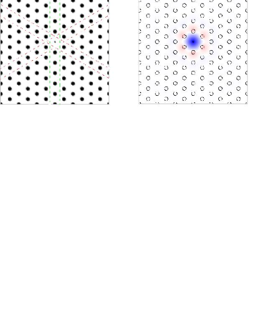
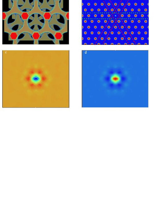
To demonstrate logic operations in 3D photonic crystals, we designed the structure [18-19] shown in Fig. 10a. The 3D photonic crystal we have chosen has various advantages over others [20-22]: emulation of 2D properties in 3D [19], polarization of the modes, and simplified design and simulation. It consists of alternating layers of a triangular lattice of air holes and a triangular lattice of dielectric rods, where the centers of the holes are stacked along the [111] direction of the face-centered cubic (fcc) lattice. The parameters for the crystal are given in the caption of Fig. 10a. We calculated that the structure exhibits a 3D band gap of over , across the frequency range of - .
As in the 2D geometry, we introduce a defect by reducing the radius of a rod inside the crystal as shown in Fig. 10b. Using the supercell method we computed that this cavity supports only a single mode with a frequency of . Setting tunes the cavity mode to the atomic transition wavelength of . Thus we can design a 3D single-mode cavity for our system to operate as the desired quantum logic gates.
The spatial profile for the electric field of the mode is shown in Figs. 10c and 10d. Note that it has similar profile with its 2D counterpart in Fig. 6b, where the energy density is also maximized in the center of the cavity. It is this similarity which simplifies our design and analysis for the 3D case.
We can quantify [19] the TM-polarization of the mode in a plane as:
| (28) |
We compute that is almost in the defect plane shown in Fig. 10b for the spatial profile exhibited in Figs. 10c and 10d. Then it is safe to assume TM polarized mode in the system Hamiltonian, because this doesn’t affect the probability amplitudes significantly in the microwave regime, for the parameters we have chosen.
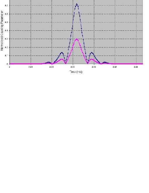
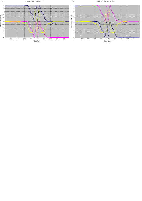
The coupling parameters as function of time in the reference frame of atoms are shown in Fig. 11, where the velocities of atoms are set to be at .
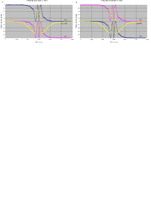
In Fig. 12 we demonstrate the 3D version of our 2D dual-rail Hadamard gate, which also acts as an atomic entangler. Similarly to the 2D case, if the excitation is on atom , the resulting state is [see equation (19)] as shown in Fig. 12a, while it is on atom the output state is [see equation (20)] as displayed in Fig. 12b, up to an unimportant global phase of . Interaction between atom and is mediated by the photonic qubit when correct parameters are set.
We set the velocity of both atoms to to obtain a dual-rail NOT gate in the 3D photonic crystal, up to an unimportant global phase factor, . The probability amplitude evolution of the atoms is displayed in Fig. 13.
The excitation of the excited atom is transferred to the ground state atom with the help of the photonic qubit allowed in the designed cavity. Note that because of the symmetry of the problem, the s in Figs. 5a, 9a and 13a are indeed approximately the same as the s of Figs. 5b, 9b and 13b, respectively. Furthermore, for the same reason as in the 2D case, analyzed above, our 3D dual-rail NOT gate also operates as a SWAP gate up to some deterministic phase. That is,
| (29) |
| (30) |
| (31) |
| (32) |
Note also that the velocities of the atoms and for the 2D logic gates agree more than with those in 3D. This makes sense due to the fact that the localized modes allowed in 2D and 3D cavities, respectively, which we considered above, have more than overlap in their spatial profiles [19]. Thus our results are also consistent with ref. [19] and this is another reason, why we first investigated 2D case.
5 Conclusions
To summarize, photonic band gap materials could be especially promising as robust quantum circuit boards for the delicate next generation quantum computing and networking technologies. The high quality factor and extremely low mode volume achieved successfully in microcavities have already made photonic crystals an especially attractive paradigm for quantum information processing experiments in cavity QED [1,2,7]. In our paper we have extended this paradigm by solving analytically the Jaynes-Cummings Hamiltonian under dipole and rotating wave approximation for two syncronized two-level atoms moving in a photonic crystal and by applying it to produce the two maximally entangled states in equations (19) and (20). We have also demonstrated the design of quantum logic gates, including dual-rail Hadamard and NOT gates, and SWAP gate operations. Our proposed system is quite tolerant to calculation and/or fabrication errors. Furthermore, most errors left beyond the design can also be easily circumvented by simply adjusting the velocity or the angle between the atomic moment vector of atoms and the mode polarization in experiments. Our technique could not only be generalized to -atom entanglement [2] but also has potential for universal quantum logic gates, atom-photon entanglement processes, as well as the implementation of various, useful cavity QED based quantum information processing tasks. We should also mention the methodological result that thanks to the emulation of 2D photonic crystal cavity modes in 3D photonic crystals [19], one can design the more sophisticated circuit first in 2D to reduce difficulty of the 3D computations where typically much more computational power is needed.
References
- [1] N. Vats et al, “Quantum Information Processing in Localized Modes of Light within a Photonic Band-gap Material”, J. Mod. Opt. 48, 1495 (2001).
- [2] M. Konopka and V. Buzek, “Entangling Atoms in Photonic Crystals”, Eur. Phys. J. D 10, 285 (2000).
- [3] M. A. Nielsen and I. L. Chuang, “Quantum Information and Quantum Computing", Cambridge University (2000).
- [4] J. D. Joannopoulos et al, “Photonic Crystals: Molding the Flow of Light”, Princeton University Press (1995).
- [5] D. Ö. Güney et al, “Design and Simulation of Photonic Crystals for Temperature Reading of Ultra-small Structures”, 2001 IEEE/LEOS Annual Meeting Conference Proceedings 1, La Jolla, CA, USA.
- [6] O. Painter et al, “Two-dimensional Photonic Band Gap Defect Mode Laser”, Science 284, 1819 (1999).
- [7] J. Vuckovic et al, “Design of Photonic Crystal Microcavities for Cavity QED”, Phys. Rev. E 65, 016608 (2001).
- [8] S. John and J. Wang, “Quantum Optics of Localized Light in a Photonic Band Gap”, Phys. Rev. B 43, 12772 (1991).
- [9] J. J. Sakurai, “Modern Quantum Mechanics”, Addison-Wesley (1994).
- [10] M. Tavis and F. W. Cummings, “Exact Solution for N-Molecule-Radiation Field Hamiltonian”, Phys. Rev. 170, 379 (1968).
- [11] P. R. Villeneuve et al, “Microcavities in Photonic Crystals: Mode Symmetry, Tunability, and Coupling Efficiency”, Phys. Rev. B 54, 7837 (1996).
- [12] Private communication with J. Vuckovic of the Stanford University.
- [13] H. J. Kimble, “Strong Interactions of Single Atoms and Photons in Cavity QED”, Physica Scripta T76, 127 (1998).
- [14] S. Haroche and J. M. Raimond, in “Cavity Electrodynamics”, edited by P. Berman, Academic Press 1994.
- [15] Y. Yamamoto and A. Imamoglu, “Mesoscopic Quantum Optics”, Wiley-Interscience Publication 1999.
- [16] R. J. Glauber and M. Lewenstein, “Quantum Optics of Dielectric Media”, Phys. Rev. A 43, 467 (1991).
- [17] S. G. Johnson and J. D. Joannopoulos, “Block-iterative Frequency-domain Methods for Maxwell’s Equations in a Planewave Basis”, Opt. Exp. 8, 173 (2001).
- [18] S. G. Johnson and J. D. Joannopoulos, “Three-dimensionally Periodic Dielectric Layered Structure with Omnidirectional Photonic Band Gap”, Appl. Phys. Lett. 77, 3490 (2000).
- [19] M. L. Povinelli et al, “Emulation of Two-dimensional Photonic Crystal Defect Modes in a Photonic Crystal with a Three-dimensional Photonic Band Gap”, Phys. Rev. B 64, 075313 (2001).
- [20] S. Fan et al, “Design of Three-Dimensional Photonic Crystals at Submicron Lengthscales”, Appl. Phys. Lett. 65, 1466 (1994).
- [21] K. H. Dridi, “Intrinsic Eigenstate Spectrum of Planar Multilayer Stacks of Two-Dimensional Photonic Crystals”, Opt. Exp. 11, 1156 (2003).
- [22] K. H. Dridi, “Mode Dispersion and Photonic Storage in Planar Defects within Bragg Stacks of Photonic Crystal Slabs”, J. Opt. Soc. Am. B 21, 522 (2003).
- [23] Y. Mu and C. M. Savage, “One-atom Lasers”, Phys. Rev. A 46, 5944 (1992).
- [24] T. B. Pittman and J. D. Franson, “Cyclical Quantum Memory for Photonic Qubits”, Phys. Rev. A 66, 062302 (2002).