A finite element analysis of a silicon based double quantum dot structure
Abstract
We present finite-element solutions of the Laplace equation for the silicon-based trench-isolated double quantum-dot and the capacitively-coupled single-electron transistor device architecture. This system is a candidate for charge and spin-based quantum computation in the solid state, as demonstrated by recent coherent-charge oscillation experiments. Our key findings demonstrate control of the electric potential and electric field in the vicinity of the double quantum-dot by the electric potential applied to the in-plane gates. This constitutes a useful theoretical analysis of the silicon-based architecture for quantum information processing applications.
pacs:
85.35.Be, 03.67.LxRecent experiments conducted on trench-isolated double quantum-dot (IDQD) structures have successfully demonstrated detection of single-electron polarization,Emiroglu:03 and coherent-charge oscillation.Gorman:05 This highlights the possibility of constructing charge-based quantum computer circuits in Si, with coherence times of the order ns.NielsonBook ; Loss:98 The architecture for a single qubit device is a complex, three-dimensional structure consisting of a single-electron transistor (SET), an IDQD, and gate electrodes. This makes it difficult to determine theoretically the system evolution by means of a complete and self-consistent Schrödinger-Poisson analysis. This is particularly the case if the analysis were to fully take into account the device geometry and all interactions while performing quantum manipulations within the coherence time of the qubit.ft1
In this paper, we present a significant contribution to such an analysis by a finite-element solution of the Laplace equation with the three-dimensional device geometry and material composition taken into account. The aim of this work is to demonstrate the electrostatic effect on the IDQD structure when voltages are applied to the in-plane control gates of the device.
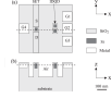
Figures 1(a) and 1(b) show device schematics in the - and --planes, respectively. The trench isolation, illustrated in Fig. 1(b), is formed by high-resolution electron-beam lithography and reactive-ion etching. Each trench is approximately nm deep and runs into the buried-oxide (BOX) layer of the silicon-on-insulator (SOI) wafer. The active regions of the device elements are P doped Si, which are electrically isolated from other device elements, as seen in Fig. 1. In this work, we use rectangular approximations to the device elements and the etched profiles to simplify the analysis.ft2
The small dimensions of the quantum dots and the nm constriction between them, which is fully depleted and acts as a tunable inter-dot tunnel barrier, result in a significant double-well type confinement potential for the electrons that occupy discrete quantum states on each quantum dot.Fujisawa:98 ; vanDerWiel:02 The tunable inter-dot coupling causes the wave functions in the two dots to overlap and hybridize so that they may be thought of as pseudo-molecular states of an artificial two atom molecule. The IDQD is an electrically-isolated component that is coupled only capacitively to the rest of the circuit, including the SET for read-out, and the in-plane control gates (G1 to G3) for manipulation. Voltages applied to the gates G1 to G3 are used to tune the electric field in the vicinity of the IDQD, and thus, the confinement potential asymmetry and inter-dot tunnelling. Hence, an electron initially localized on one quantum dot may be allowed to tunnel to the opposite quantum dot by such manipulation.
An electric field is induced on the SET as a result of this polarization process. This modulates the chemical potential of the SET, and, therefore, the conductance through the source and drain leads under a finite SET bias condition. To maximize the change in conductance, the SET is initially tuned to the charge-sensitive regime by an appropriate voltage bias at G4, and under a small source-drain bias to ensure operation in the linear transport regime. Such manipulation of the device has only been shown through experiment so far. Therefore, a thorough theoretical analysis is necessary to complement the recent experimental findings, and build a more comprehensive understanding of the physical mechanisms involved.
Analytic methods exist for calculating the electrostatic potential in two-dimensional electron gases generated by patterned surface gates on GaAs/AlGaAs heterostructures.Davies:94 ; Davies:95 While these analytic methods yield useful results for such devices, they are unsuitable for trench-isolated Si structures, where the geometry is much more sophisticated. Therefore, numerical methods have to be implemented. The finite-element method is a well-suited means for simulation of geometrically-complicated domains,Cook ; Zienkiewicz and is commonly used to solve Poisson-type equations.Iserles ; DpBook2
In order to determine the electric field throughout the modelled device regions, the numerical solution to the Laplace equation in three-dimensions is performed:
| (1) | |||||
| (2) | |||||
| (3) |
where is the electrostatic potential and is the material dielectric parameter. The dielectric parameter varies discontinuously on moving through the different materials - air (Fm-1), Si () and SiO2 (). We apply Dirichlet boundary conditions to the surfaces of the metal gates and to the grounded base of the device, and the Neumann boundary condition to the exposed surfaces. (We apply Neumann boundary conditions with , but for generality, we include in our discussion the possibility of non-zero ).
The finite element solution of the Laplace equation is well covered in the literature.Iserles ; DpBook2 ; Mohan The basic idea of the finite element method is to approximate the unknown fields, for example in the Laplace equation above, by which is a combination of linearly independent basis functions
| (4) |
where is the number of basis functions and are the expansion coefficients to be determined. In the finite element method, the computational domain is divided into a number of elements, and the are chosen to be piecewise polynomials such that they are non-zero only in a ‘few’ adjacent elements.ft3 ; Iserles The method then requires the substitution of into the Laplace equation, and the residual to be orthogonal to the space spanned by a linearly independent set . In our calculations, we implement the orthogonality through the weighted residual statement:
| (5) |
and Galerkin’s method i.e. set equal to the basis functions to obtain
| (6) |
Using integration by parts, we reduce the order of derivatives in Eq. (6);
| (7) |
The weighted residual method and integration by parts leads to a natural mechanism for the incorporation of derivative boundary condition given by Eq. (3) for the Laplace operator . Hence, we obtain after expanding the approximation for
| (8) |
where summation is implied over repeated indices. The problem has now been reduced to one of matrix inversion;
| (9) |
where the ‘stiffness’ matrix is given by
| (10) |
and the RHS vector is given by
| (11) |
and is simply the vector of unknowns . Dirichlet boundary conditions are implemented by forcing prescribed values of .
In the formulation and solution of Eq. (9) we have chosen linear basis functions corresponding to 8-noded brick elements. This method therefore has a convergence rate for error of 2.0.ft4
We have employed Gaussian quadrature in three-dimensions for the volume integrals and two-dimensions for surface integrals, and a conjugate gradient method with Incomplete Lower and Upper (ILU) factorization preconditioning to solve the resulting linear system of equations. Sufficient resolution was obtained by a mesh with nodes in the , and directions, respectively. We implemented adaptive mesh refinement along axis to improve accuracy in the vicinity of the active region.
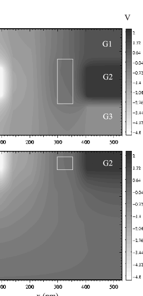
Figures 2(a) and 2(b) show cross-sectional slices along orthogonal planes of the full three-dimensional solution for the simulated electric potential. The simulation was performed with the following parameters: the gate potentials of G1, G2 and G3 are set to + V, V and - V, respectively; G4 is set to V. The voltage chosen for G4 is approximately equal to that used for this gate in the experimental demonstrations in Ref. Emiroglu:03, where single electron polarization of the IDQD was obtained for such a device. The choices of G1, G2 and G3, are also similar to those in the experiments but for this simulation, the exact values are chosen so that three-dimensional illustrations are as clear as possible.
Figures 2(a) and 2(b) clearly demonstrate the effect of the applied gate voltages on the potential landscape of the IDQD and the device as a whole; the result of applying a voltage on the in-plane gates is that a significant fraction of the applied voltage is induced on the IDQD, despite the etched trench gap. The abrupt change in the effective permittivity from the metallic gates to the voids, from the voids to the SiO2, and from Si to SiO2, causes some definition of the gates and the IDQD in the plots. The difference between the relative permittivity of air, Si and SiO2 leads to a potential gradient, such that the absolute value of the potential is prone to vanish more rapidly in air, compared with Si and SiO2. However, Fig. 2(b) clearly demonstrates that for this particular pillar height, which matches the device used in experiment, the potential at the IDQD is due mainly to the electric field vectors that are on a direct path through the trench isolation, and not the underlying substrate. This is consistent with experimental observations and is the preferred mechanism of device operation, since it is relatively easier in design and theoretical analysis, compared with the case where the majority of the electric field is through the semiconductor base and the field lines arrive at the IDQD from several different paths.
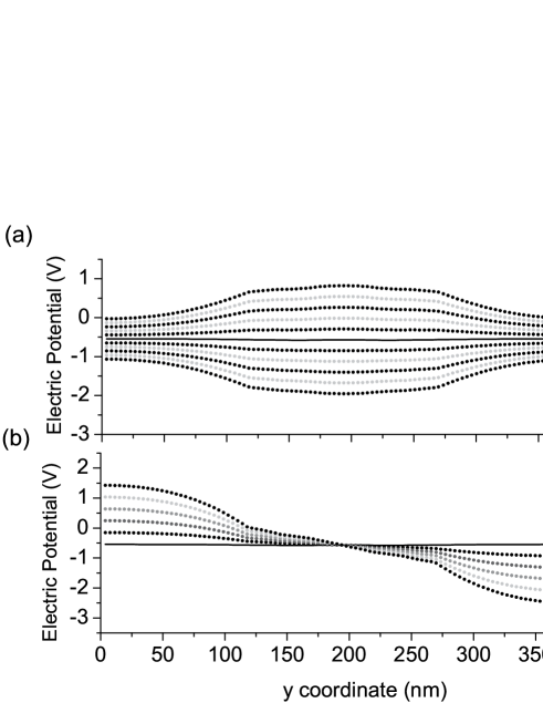
For a more quantitative analysis, we determine the electric potential along the active region of the IDQD as a function of the applied gate voltages. This is shown in Figs. 3(a) and 3(b), where different gates are used to apply the in-plane electric field. Figure 3(a) shows that the effect of varying the voltage applied to gate G2, from - V to + V, is to induce a voltage at the IDQD from - V to + V, respectively. Note that G4 had lowered the overall potential by approximately V in this case.
The data in Fig. 3(a) shows a maximum change of V of the electrostatic potential at the IDQD, when the G2 gate voltage is raised or lowered by V. This field coupling factor of is approximately one order of magnitude greater than what was observed in experiment.Emiroglu:03 However, the measured quantity in experiments is the SET current, and the IDQD coupling terms are inferred from such measurements. The task of calculating such coefficients exactly as measured in experiment is beyond the scope of a purely electrostatic model, since, with the SET present, the global system that must be treated consists of interacting sub-systems of quantum mechanically bound electrons. Therefore, we project that a self-consistent Schrödinger-Poisson analysis of the system would yield results for the coupling coefficients that are closer to actual values observed in experiment.
Our results are also consistent with the experimental demonstrations of Ref. Emiroglu:03, where the voltage on gate G2 is swept continuously from V to V, with G4 set to V, in order to demonstrate conductance resonances of the SET currents but also resonances due to the single electron polarization of the IDQD. (The device in Ref. Emiroglu:03, had a slight asymmetry in the alignment of the IDQD relative to G2, hence the ability of G2 to polarize the IDQD.)
The abrupt changes in the potential at nm and nm are due to the change of relative permittivity at the air-SiO2 interface. The difference between the potential gradient in the air and in the semiconductor regions is more evident in these figures. Figure 3(b) shows the effect of applying voltages of opposite sign to gates G1 and G3. This results in a potential gradient across the IDQD, which has a maximum value of Vnm-1 in these simulations. This clearly demonstrates an effective mechanism for externally tuning the internal potential asymmetry of the IDQD electronic states.
In the experimental demonstrations of Ref. Gorman:05, , a voltage bias is pulsed across in-plane metallic gates, which are placed perpendicularly to an IDQD as in our case, and this was shown to result in the coherent oscillation of a single electron charge present in an IDQD. This is again consistent with our results which suggests a strong electric field is induced at the IDQD due to the electric field at the in-plane gates.
In summary, we have successfully demonstrated, by means of finite-element solutions to the Laplace equation, that the electric potential and potential gradient across the confining region of the IDQD in trench-isolated Si devices may be manipulated effectively by the voltages applied to capacitively-coupled in-plane gates. Our calculations show good correlation with recent experimental demonstrations, where the IDQD electron states are manipulated by such methods.
We thank S. Pfaendler and R. Schumann for comments and useful discussions. SR, JG, and CB acknowledge the support of the EPSRC through the QIP IRC. SR acknowledges the Cambridge-MIT Institute for financial support.
References
- (1) E. G. Emiroglu, D. G. Hasko and D. A. Williams, Appl. Phys. Lett. 83, 3942-3044 (2003).
- (2) J. Gorman, D. G. Hasko and D. A. Williams, Phys. Rev. Lett. 95, 090502 (2005).
- (3) D. Loss and D. P. DiVincenzo, Phys. Rev. A 57, 120-126 (1998).
- (4) M. A. Nielsen and I. L. Chuang, Quantum Computation and Quantum Information, Cambridge University Press, (2003).
- (5) The most significant interaction is that between the SET and the IDQD because it directly influences the read-out operation and the degree of back-action.
- (6) The device elements are in fact roughly rectangular, so this approximation introduces only a small error to the results presented.
- (7) W. G. van der Wiel, S. De Francheshi, J. M. Elzerman, T. Fujisawa, S. Tarucha and L. P. Kouwenhoven, Reviews of Modern Physics, 75, 1-22, (2003).
- (8) T. Fujisawa, T. H. Oosterkamp, W. G. van der Wiel, B. W. Broer, R. Aguado, S. Tarucha and L. P. Kouwenhoven, Science, 282, 932-935, (1998).
- (9) J. H. Davies, I. A. Larkin and E. V. Sukhorukov J. Appl. Phys. 77, 4504-4512 (1995).
- (10) J. H. Davies and I. A. Larkin, Phys. Rev. B 49(7), 4800-4809 (1994).
- (11) R. D. Cook, D. S. Malkus and M. E. Plesha, Concepts and Applications of Finite Element Analysis, Wiley, (1989).
- (12) O. Zienkiewicz, The Finite Element Method, McGraw-Hill, 4th edition (1994).
- (13) A. Iserles, A first course in the numerical analysis of differential equations, Cambridge University Press, (1995).
- (14) H. P. Langtangen, Computational Partial Differential Equations - Numerical methods and Diffpack Programming, Springer, 2nd edition (2003).
- (15) L. Ramdas Ram-Mohan, Finite Element and Boundary Element Applications in Quantum Mechanics, Oxford University Press, 1st edition, (2002).
- (16) The choice of piecewise polynomials results in a speed-up over spectral methods with little increase in error.
- (17) Higher-order basis functions were also implemented but had not resulted in any significant improvement in the accuracy of the results presented.