The ultra–sensitive electrical detection of
spin Rabi oscillation at paramagnetic defects
Abstract
A short review of the pulsed electrically detected magnetic resonance (pEDMR) experiment is presented. PEDMR allows the highly sensitive observation of coherent electron spin motion of charge carriers and defects in semiconductors by means of transient current measurements. The theoretical foundations, the experimental implementation, its sensitivity and its potential with regard to the investigation of electronic transitions in semiconductors are discussed. For the example of the center at the crystalline silicon (111) to silicon dioxide interface it is shown experimentally how one can detect spin Rabi-oscillation, its dephasing, coherence decays and spin–coupling effects .
pacs:
71.55.-i 72.20.Jv 76.90.+d 72.25-bI Introduction
Electron spin resonance (ESR) has proven in the past to be a useful characterization method for the microscopic investigation of paramagnetic semiconductor defects. The limitations of ESR spectroscopy on semiconductors is set by its sensitivity. Wavelengths in the microwave range are too long to be detected as single photons. Thus, as low dimensional semiconductors and mesoscopic structures such as quantum–wells, -dots or -wires or semiconductor thin films have increasingly become subjects of research, ESR spectroscopy that typically reaches sensitivity limits of the order of spins for semiconductor samples at the widely used X-Band (GHz), is hardly applicable anymore.
In order to achieve higher sensitivities, magnetic resonance methods have been combined in the past with other measurement techniques such as force microscopy Rugar:2004 , photoluminescence Jelezko:2002 ; Jelezko:2004 or conductivity measurements Kouven:2004 ; Jiang:2004 which have all reached single spin detection sensitivity in recent years. Among these methods, the electrically detected magnetic resonance (EDMR) technique may be most beneficial for the spin spectroscopy of semiconductors since naturally, it is very sensitive to centers which influence conductivity while it is blind to all other spins. For most of the EDMR studies found in literature, including those reporting on a single spin detection, the experiments were conducted as pure continuous wave (cw) measurements; Pulsed (p) EDMR experiments have only been demonstrated recently Boediss ; Boe7 . Since pEDMR combines the advantages of pulsed ESR with those of cw EDMR, these first results suggest that new insights can potentially be found for the many materials on which cw EDMR has been performed in the past. Beyond material spectroscopy, pEDMR is also expected to play a role for semiconductor based quantum information concepts: So far, only electrical single spin detection but not electrical single spin readout experiments have been demonstrated Kouven:2004 ; Jiang:2004 . A readout of a single spin requires a coherent spin measurement that allows to distinguish between different eigenstates. A requirement which can only be met by coherent spin–detection schemes as used for pEDMR experiments.
In the following, a brief review of the theoretical and experimental foundations of pEDMR experiments is given. It is shown how one can access coherent spin–Rabi oscillation by means of electric currents and how this observation can reveal insights into the nature of the observed defect centers. The sensitivity limitations of pEDMR are addressed, too. As model system, centers located at the crystalline silicon (c-Si) (111)/silicon dioxide () interface are used.
II Theoretical background
PEDMR takes advantage of the spin dependency of charge carrier transitions in semiconductors which occurs when spin conservation is imposed on electronic transitions. Spin–dependent transition rates between paramagnetic centers can be described in terms of a spin pair ensemble consisting of pairs of two spins with corresponding to the two states between which transitions occur KSM ; HabDie ; Boe6 . The transition rates will be proportional to the singlet content and thus, by measuring currents as a function of time, the evolution of can be accessed.
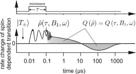
The challenge for pEDMR measurements is to detect very small current changes with high time resolution on top of comparatively large constant current offsets. It is usually impossible to attain a time resolution with electrical measurements that is within the coherence time of the spin systems and that is at the same time sensitive enough to detect the subtle signal currents. This contradiction between sensitivity and time resolution is solved for pEDMR with an indirect detection scheme Boediss ; Boe7 ; Boe6 ; Boe3 ; Boe9 where the change of the photocurrent after a coherent pESR excitation is measured as a function of the length of the resonant pulse. A sketch of this measurement principle is illustrated in fig. 1: The experiment begins when the steady state ensemble that, due to the short singlet lifetimes, consists mainly of pure triplet eigenstates, is coherently manipulated and brought into a non–steady state, non–eigenstate which is determined by , the microwave field strength and the microwave frequency . After the excitation, the non–eigenstates will carry out a Larmor precession whose influence on the net transition rate will fade quickly due to the ensemble dephasing Boe1 . Thus, a short time after the end of the microwave pulse, a non–steady state transition rate is present that relaxes slowly (on a s to ms time scale) back to the steady state. It is known Boe6 that the integral of this relaxation current, , is proportional to the the density change
| (1) |
wherein and are the density matrix and the steady state density matrix elements, respectively and , and correspond to the exchange coupling, the dipolar coupling and the Larmor separation within the pairs, respectively Boe6 ; Boediss . Because of this, is a function of the ensemble state right at the end of the pulse and thus, it is possible to determine the evolution of during the excitation by measuring as function of . The time resolution of this measurement scheme is obviously not determined by the current amplifier but by the pulse length generator and thus, a low ns–range time resolution is technically easy to achieve.
For the detection of spin–Rabi oscillation during the coherent excitation, can be recorded when is strong enough so that Rabi frequencies are larger than the coherence time of the spin pairs and is in ESR with a selected defect or impurity. A quantum mechanical description of this experiment Boe6 has revealed an expression
| (2) |
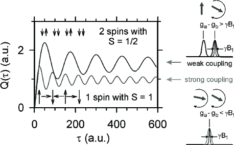
under the assumption of homogeneous fields and a sufficiently smooth line shape of the spins in resonance which means . In eq. 2, pair partner has a Landé factor, , and is exposed to an external magnetic field whereas denotes a factor whose value depends on the spin–spin coupling within a pair. An illustration of two of these coupling cases based on a theoretical calculation Boe6 is given in fig. 2. Weak coupling () implies that an ESR excitation can always manipulate either spin a or spin b, depending on the chosen excitation frequency . Hence, the Rabi oscillation reflects the transient nutation of a simple electron spin and therefore, . When the coupling is strong (), the excitation is not selective for any pair partner anymore and hence, two electron spins are turned and . The transients plotted in fig. 2 where calculated under negligence of incoherence. The decay of the oscillation is due to the gradual spectral narrowing of the excitation width with increasing .
In addition to the two coupling cases illustrated in fig. 2, another case shall be mentioned here: When (strong coupling) but , then . While this case has so far not been described theoretically for pulsed EDMR experiments, one can deduce it from the description of transient nutation experiments of systems without hyperfine influences as given by Astashkin and Schweiger schweiger:1990 .
III A pEDMR experiment with -centers
We have chosen recombination of photoexcited charge carriers at the well understood and well characterized -center to serve as a model system for the demonstration of pEDMR. centers are trivalent Si atoms at the c-Si/SiO2 interface. They dominate interface trapping and recombination, they are paramagnetic when uncharged Poin:1981 ; Poin:1984 and they are strongly localized, anisotropic electronic states lena:1998 . For the c-Si (111) surface orientation, all centers point into a direction perpendicular to the interface. Because of this, their microscopic anisotropy is reflected by the ESR as well as EDMR spectra as shown repeatedly in the literature lena:1998 ; Friedrich:2004 . First pEDMR studies at the -center have been carried out recently by Friedrich et al. Friedrich:2004 which revealed that charge carrier trapping and recombination can take place without the presence of additional shallow trapping centers through a two step trapping/readjustment direct capture process that had been described theoretically first by Shockley and Read shoc:1952 and later Rong et al. rong2 .
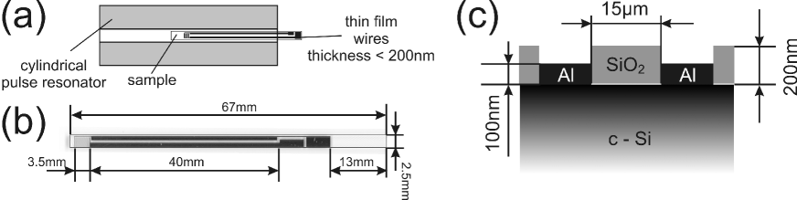
In order to conduct pEDMR, a semiconductor sample must be placed inside a microwave resonator such that the field about the centers that are to be excited can be generated. Since electrical contacts naturally consist of conducting material, they may alter the eigenmodes of a microwave cavity whose geometry was designed under the assumption that the fill–factor of conducting material therein is negligible. The uncontrolled change of eigenmodes leads to a strong inhomogeneity of throughout the resonator, especially at the sample position. This causes a rapid, artificially induced dephasing of the spins in resonance and thus, the observation of Rabi oscillation becomes impossible. Thus, the sample and especially the contacts must be designed such that a distortion is as small as possible. One can achieve this with sample substrates whose conductivity is as low as possible and sample contacts with thicknesses below the microwave penetration depth. An example for such a complete thin film contact wiring of the sample within the microwave resonator is illustrated in fig. 3(a) to (c). In (a), a sketch of a thin film wired sample within a cylindrical microwave resonator is shown. While the actual semiconductor sample with its interdigited contact grid is located at the tip of the match–like substrate in the center of the cavity, it is connected to the contact pads on the outside by 40 mm long and less than 200 nm thin Al stripes. Figure 3(b) displays a photo of an acutal thin–film wire and contact structure. One can see the structure and its dimensions with contact pads, wires and grids. The grid area consists of 75 grid pairs where each grid has 5 m width and 15 m distance to its respective neighbors as indicated in fig. 3(c). With the sample and contact geometry given, one can (i) minimize sample resistances and therefore maximize sample currents, time resolution and sensitivity and (ii) the actual semiconductor sample will be at the center of the cavity where has its maximum, while (iii) the eigenmodes of the cavity especially at its center remain undistorted.
The sample used for the experiment was made from a 380 m thick (111) surface oriented, slightly phosphorous doped ( 10 cm) Czochralski grown c-Si wafer whose surface was subjected to an RCA cleaning procedure followed by the formation of an about 200 nm thick thermal oxide layer. The oxide was formed at 1050 oC under exposure of the sample to O2 for 200 min. The thickness of the resulting oxide was confirmed by profilometer measurements. After the oxide formation, the contact and wire system was deposited by means of a photolithographic lift–off procedure before the wafer was cut into match–like stripes. The current detection and coherent microwave excitation as well as the extraction of spin–dependent currents from microwave induced currents was executed with the same setup and the same procedure as described in Refs. Boediss and Boe7 .
All experiments presented in the following were performed at a sample temperature of K and a sample
irradiation of 0.2(1) W/cm2 with Ar+ laser light ( nm). For the coherent excitation, a Bruker E580 X-Band pulse ESR spectrometer was used. A photocurrent of A was established by a constant current source with long dwell time (1 s) to allow for a drift compensation. In order to measure the charge , the current was then subtracted by the constant offset before it was transformed by an impedance changer into a voltage signal which was then filtered by a high pass and subsequently digitized by an 8 bit transient recorder. The integration took place between 14 s and 30 s after the pulse which is the part of the photocurrent relaxation transient where the current signal reached its maximum.
The signal to noise ratios (SNR) per charge carrier pair, which poses an upper limit for the spin sensitivity since several charge carrier pairs can undergo transitions at one defect, was at 250 W microwave power with n being the number of accumulated transients. Thus, within an 8 hour period and 300 s shot repetition time, one can attain a sensitivity of a few hundred charge carriers. This sensitivity is about 9 orders of magnitude higher than conventional ESR measurements under comparable conditions, yet it is still not a single spin or even a single spin per single shot sensitivity. The reason for this limit is the presence of strong artifact currents within the sample due to the application of the strong microwave pulses. It is therefore not a principle limitation of the measurement method but due to the sample design. A further downscaling of the sample area and the prevention of shunt currents due to diffused excess charge carriers into the c-Si bulk could push the sensitivity even further.
IV Experimental results
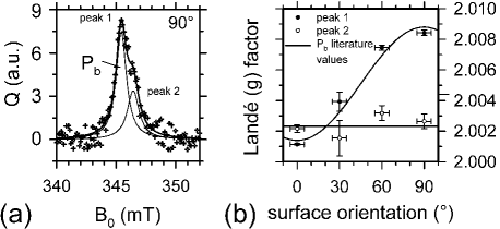
We have recorded as a function of the strength of the external magnetic field as well as the angle between and the c-Si (111) orientation of the sample in order to confirm that the measured signals are due to electronic transitions at centers. Figure 4(a) displays this for a sample orientation of 90∘ which was recorded after an excitation with ns and a microwave power of 4 W. The data was fit with two Lorentzian line shapes. One can see that peak 1 has a much stronger intensity in comparison to peak 2. The measurement represented by fig. 4(a) was repeated for sample orientations with angles of 60∘, 30∘, and 0∘. In all cases, the data could be fit reasonably with two Lorentzians. The factor of all fits are displayed in fig. 4(b) and show that peak 1 has the anisotropy of the centers as it can be found in the literature lena:1998 and as it is shown by the solid line. We therefore assign peak 1 to the center. Peak 2 shows no identifyable anisotropy.
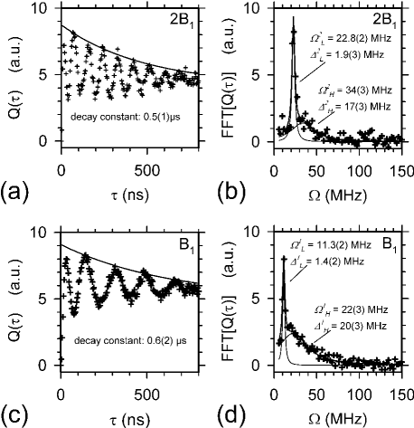
For the electrically detected spin–Rabi oscillations, the sample orientation was turned back into the 90∘ position since then, the two peaks were well separated such that an excitation of peak 2 was minimized. The microwave frequency and the external field where adjusted such that the peak maximum at was on resonance. Then, was changed between 0 and 800 ns in 2 ns steps. The resulting transients are displayed in fig. 5(a) and (c) for applied microwave powers of 250W and 62W, respectively. This corresponds to arbitrary microwave fields and , respectively. One can clearly see the oscillatory behavior of in both plots.
The maxima in the plots (a) and (c) of fig. 5 were fit with simple exponential decay functions. The two fits agree within the margin of error and reveal a time constant of ns. In order to determine the frequency components of the two data sets, they were subjected to fast Fourier transforms (FFT) whose absolute results are plotted in fig. 5(b) and (d) for the microwave fields and , respectively. The data of both plots was fit with two Lorentzians with the fit plotted in the graphs. Note that, within the margin of error, the exponential decay functions of fig. 5(a) and (c) agree with the fit results for the width of the peaks with lower frequency and in the FFT plots (b) and (d) which shows that the lower frequency component belongs to the slowly decaying process.
V Discussion of results
We have shown that it is possible to observe coherent spin–Rabi oscillation by means of transient current measurements. This shows that distinct eigenstates of spins in semiconductors can be read electrically. One can interpret the data presented ins figs. 4 and 5 by taking advantage of Rabis formula Boe6 , wherein is expressed in gyromagnetic units. Note that when we measure on resonance. Since this is exactly the case for the center frequencies and of peak 1 as shown in fig. 5(b) and (d), one can conclude that the slowly decaying oscillation is solely due to spin–Rabi oscillation involving the center. For the higher, broadly distributed frequencies centered around and this is different: From Rabis formula, we learn that when we measure off–resonant at arbitrary Rabi frequencies and with two different fields with ratio , the Larmor–frequency difference can be calculated as
| (3) |
With regard to the data in fig. 5 where , this means that mT for the broad peaks in fig. 5(b) and (d) and thus, we can conclude, that the process responsible for these peaks can be associated with peak 2 of fig. 4(a) whose Larmor–frequency was about 0.9mT higher than the excitation frequency .
Another consequence of Rabis formula mentioned above is that when we have different frequency components and in one measurement, we can obtain the ratio of their coupling factors
| (4) |
from two measurements 1 and 2 collected at two arbitrary but different fields. Note that eq. 4 is independent of the Larmor–frequency difference which means it does not play a role whether the pair centers are on or off resonance. Thus, when the fit results of fig. 5(b) and (d) are plugged into eq. 4 we obtain . With the margin of error for given, one can not distinguish whether or . However, since the mechanism associated with peak 1 has been attributed to a direct capture process into strongly coupled pairs in the past Friedrich:2004 , it becomes clear that the process associated with peak 2 must involve strongly coupled pairs, too.
VI Summary
The ultra–sensitive electrical detection of electron spin–Rabi oscillation at centers has been demonstrated and it was shown how new insights into the nature of charge carrier recombination at centers can be gained. In addition, PEDMR at the c-Si/SiO2 interface showed that a second, from the –direct capture process qualitatively different spin–dependent transition exits. With the used sample design, the electrical measurements of coherent spin motion reached a sensitivity below 1000 spins. Since this limitation is purely due to offset and microwave artifact currents, it is conceivable that further downscaling and a different sample design may be able to shift this limit towards a coherent single spin readout.
VII Acknowledgements
We thank Kerstin Jacob for the sample preparation and Jan Behrends, Kai Petter, Felice Friedrich, Walther Fuhs and Gerry Lucovsky for inspiring discussions
References
- (1) D. Rugar and R. Budakian and H. J. Mamin and B. W. Chui, Nature (London) 430 (2004) 329.
- (2) F. Jelezko and I. Popa and A. Gruber and C. Tiez and J. Wrachtrup and A. Nizovtsev and S. Kilin, Appl. Phys. Lett. 81 (12) (2002) 2160.
- (3) F. Jelezko and T. Gaebel and I. Popa and A. Gruber and J. Wrachtrup, Phys. Rev. Lett. 92 (7) (2004) 076401–1.
- (4) J. M. Elzerman and R. Hanson and L. H. Willems van Beveren and B. Witkamp and L. M. K. Vandersypen and L. P. Kouwenhoven, Nature (London) 430 (2004) 431.
- (5) M. Xia and I. Martin and E. Yablonovitch and H. W. Jiang, Nature (London) 430 (2004) 435.
- (6) Christoph Böhme, Dynamics of spin–dependent charge carrier recombination, Cuvillier Verlag, Göttingen, 2003.
- (7) C. Boehme and K. Lips, Phys. Rev. Lett. 91 (24) (2003) 246603.
- (8) D. Kaplan and I. Solomon and N. F. Mott, J. Phys. (Paris) – Lettres 39 (4) (1978) L51–L54.
- (9) R. Haberkorn and W. Dietz, Solid State Commun. 35 (6) (1980) 505–508.
- (10) C. Boehme and K. Lips, Phys. Rev. B 68 (24) (2003) 245105.
- (11) C. Boehme and K. Lips, Appl. Phys. Lett. 79 (26) (2001) 4363–4365.
- (12) C. Boehme and K. Lips, Appl. Magnetic Resonance 27 (2004) 109–122.
- (13) C. Boehme and P. Kanschat and K. Lips, Europhys. Lett. 56 (5) (2001) 716–721.
- (14) A. V. Astashkin and A. Schweiger, Chemical Physics Letters 174 (6) (1990) 595–602.
- (15) E. H. Poindexter and P. J. Caplan and B. E. Deal and R. R. Razouk, J. Appl. Phys. 52 (1981) 879.
- (16) E. H. Poindexter and G. J. Gerardi and M.-E. Rueckel and P. J. Caplan and N. M. Johnson and D. K. Biegelsen, J. Appl. Phys. 56 (10) (1984) 2844.
- (17) P. M. Lenahan and J. F. Conley, J. Vac. Sci. Technol. B 16 (1998) 2134–2153.
- (18) F. Friedrich and C. Boehme and K. Lips, J. Appl. Phys. 97 (2005) 056101.
- (19) W. Shockley and W. T. Read, Jr., Phys. Rev. 87 (5) (1952) 835.
- (20) F. C. Rong and G. J. Gerardi and W. R. Buchwald and E.H. Poindexter and M. T. Umlor and D. J. Keeble and W. L. Warren, Appl. Phys. Lett. 60 (5) (1992) 610–612.