Demonstration of an optical quantum controlled-NOT gate without path interference
Abstract
We report the first experimental demonstration of an optical quantum controlled-NOT gate without any path interference, where the two interacting path interferometers of the original proposals (Phys. Rev. A 66, 024308 (2001), Phys. Rev. A 65, 012314 (2002)) have been replaced by three partially polarizing beam splitters with suitable polarization dependent transmittances and reflectances. The performance of the device is evaluated using a recently proposed method (Phys. Rev. Lett. 94, 160504 (2005)), by which the quantum process fidelity and the entanglement capability can be estimated from the 32 measurement results of two classical truth tables, significantly less than the 256 measurement results required for full quantum tomography.
pacs:
03.67.Lx, 03.67.Mn, 03.65.Yz, 42.50.ArQuantum computing promises to solve problems such as factoring large integers SHOR97 and searching over a large database GRO97 efficiently. One of the greatest challenges is to implement the basic elements of quantum computation in a reliable physical system and to evaluate the performance of the operation in a sufficient manner. In one of the earliest proposals for implementing quantum computationMIL88 , each qubit was encoded in a single photon existing in two optical modes. The main advantage of the photonic implementation of qubits is the robustness against decoherence and the availability of one-qubit operations. However, the difficulty of realizing the nonlinear interactions between photons that are needed for the implementation of two-qubit operations has been a major obstacle. In recent work, Knill, Laflamme and Milburn (KLM) KLM01 have shown that this obstacle can be overcome by using linear optics, single photon sources and photon number detectors. By now, various controlled-NOT (CNOT) gates for photonic qubits using linear optics have been proposed KYI01 ; Pit01 ; Hof01 ; Ral01 ; Ral02 ; Nie04 and demonstrated Pit02 ; San02 ; Pit03 ; Bir03 ; Bir04 ; Zhao05 .
In particular, it has been shown in Hof01 ; Ral01 that a ‘compact’ CNOT gate can be realized by interaction at a single beam splitter and post-selection of the output. Since this gate requires no ancillary photon inputs or additional detectors, it should be especially useful for experimental realizations of optical quantum circuits. However, there have been two crucial difficulties. In the original schemeHof01 ; Ral01 , the polarization sensitivity of the operation was achieved by separating the paths of the orthogonal polarizations, essentially creating two interacting two-path interferometers. Therefore, the initial experimental realizations based the original proposal Bir03 ; Bir04 are very sensitive to the noisy environment (thermal drifts and vibrations), making it necessary to control and to stabilize nanometer order path-length differences. In addition to these problems, perfect mode-matching is required in each output of the interferometer. Thus, it is very difficult to construct quantum circuits using devices based on those experimental setups. Another difficulty is the evaluation of experimental errors in multi qubit gates. In order to obtain the most complete evaluation of gate performance possible, quantum process tomography has been used in the previous experiment Bir04 . However, 256 different measurement setups are required to evaluate only one CNOT device. When we have to evaluate even more complicated quantum devices realized by a combination of gates, the number of measurements required for tomography rapidly increases as the number of input and output qubits increases.
In this paper, we present an experimental realization of the ‘compact’ optical CNOT gate Hof01 ; Ral01 without any path interference. We show that the CNOT gate can be implemented using three partially polarizing beam splitters (PPBSs) with suitable polarization dependent transmittances and reflectances, where the essential interaction is realized by a single intrinsic PPBS, while the other two supplemental PPBSs act as local polarization compensators on the input qubits. The gate operation can then be obtained directly from the polarization dependence of the reflectances of the PPBSs, removing the need for interference between different paths for orthogonal polarizations. We have evaluated the device operation using a recently proposed method Hof04 , by which we can determine the lower and upper bounds of the process fidelity from measurements of only 32 input-output combinations. We can thus characterize the gate operation with 1/8 the number of input-output measurements required for complete quantum process tomography. We hope that these results will open a door to the realization of more complex quantum circuits for quantum computing.
Figure 1(a) shows the previously proposed optical circuit for the CNOT gate Hof01 ; Ral01 . The beam splitter sitting in the center of the circuit is the essential one which realizes the quantum phase gate operation by flipping the phase of the state , where both photons are horizontally polarized, to due to two-photon interference. Since this operation attenuates the amplitudes of horizontally polarized components by a factor of , the other two beam splitters with reflectivity 1/3 are inserted in each of the interferometer paths in order to also attenuate the amplitudes of vertically polarized components , so that the total amplitude of any two photon input is uniformly attenuated to . If we now define the computational basis of the gate as , for the control qubit, and , for the target qubit, the gate performs the unitary operation of the quantum CNOT on the input qubits.
The difficulty in the original proposal is that we have to stabilize the two interferometers of the horizontally and vertically polarized paths by controlling the length of four optical paths with an accuracy on the order of nanometers in order to achieve a reliable operation of the device. In addition, the modes in each path have to be aligned precisely at the output ports of the polarizing beam splitters. Such difficulties have been crucial obstacles for the future realization of optical quantum circuits consisting of several CNOT gates.
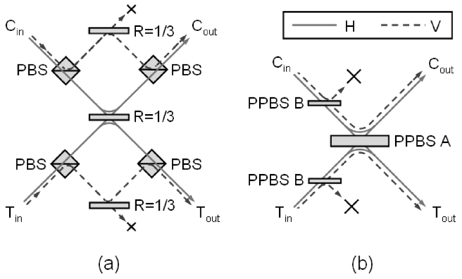
Fig. 1(b) shows our solution to this problem. We use one intrinsic PPBS (PPBS-A) and two supplemental PPBSs (PPBS-B) in the optical circuit. The intrinsic PPBS-A, which corresponds to the central beam splitter in Fig. 1(a), implements the quantum phase gate operation by reflecting vertically polarized light perfectly and reflecting (transmitting) 1/3 (2/3) of horizontally polarized light. The two supplemental PPBS-Bs are inserted to adjust the amplitudes of the local horizontal and vertical components of the photonic qubits by transmitting (reflecting) 1/3 (2/3) of vertically polarized light and transmitting horizontally polarized light perfectly. As Fig. 1(b) shows, the use of PPBSs allows us to reduce the four optical paths in Fig. 1(a) to only two optical paths, and path-interferometers are no longer required for the implementation of the ‘compact’ quantum CNOT gate.
In the following experimental demonstration, we used a simple polarization compensation instead of the two supplemental PPBS-Bs. The only purpose of the PPBS-Bs is to reduce the amplitude of the vertical component in the input to of the original input value, while leaving the horizontal component unchanged. Therefore, we can easily simulate the function of the supplemental PPBS-Bs by using compensated input states whose vertical component is reduced to . To simulate a general input state , we thus use a compensated input state of . For example, the input for the target qubit state becomes , which can be easily prepared just by changing the angle of linear polarization by rotating the /2 plate (HWP) in the target input.
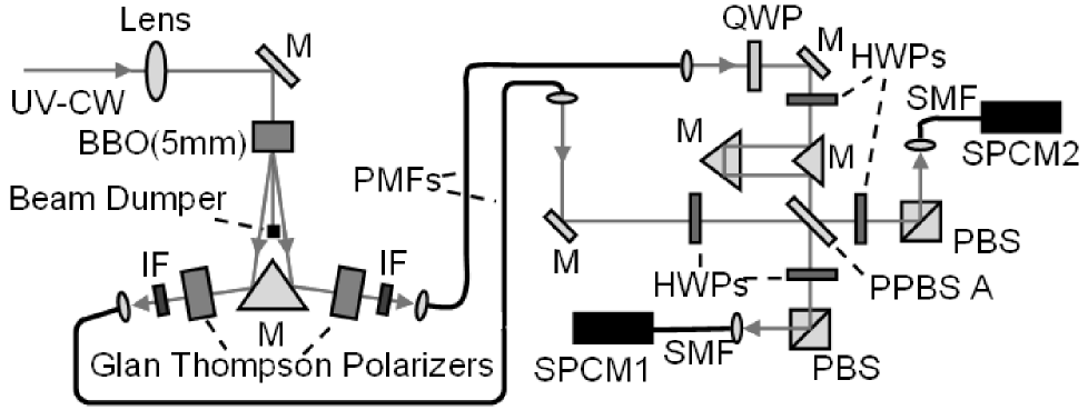
The schematic of our experimental setup is shown in Fig.2. We used a pair of photons generated through spontaneous parametric down conversion for our input. A beta barium borate (BBO) crystal cut for the type-II twin-beam condition Tak01 was pumped by an argon ion laser at a wavelength of 351.1 nm. The pump beam was focused in the BBO crystal using a convex lens to increase the photon fluxKur01 . Pairs of twin photons are emitted at 702.2 nm with orthogonal polarizations. Gland-Thompson polarizers are used to increase the extinction ratio. After removing the scattered pump light using bandpass filters (IF, center wavelength 702.2nm, FWMH 0.3nm), each of the photons was guided to polarization maintaining single-mode fibers (PMFs) via objective lens and then delivered to the CNOT verification setup. After the collimation lens for the output of the PMFs, the polarization of photons are controlled by HWPs mounted in rotating stages. The timing of the two entangled photons injected to the PPBS-A was controlled using an optical delay. A plate (QWP) was inserted to compensate the phase change between horizontal and vertical polarization in the optical delay. After the quantum interference which occurs at PPBS-A, the polarization of output photons was analyzed using HWPs and PBSs. Finally, those photons are coupled into single mode fibers (SMFs) and counted by the single photon counters (SPCM-AQ-FC, Perkin Elmer).
Our setup permits us to select various linear polarizations for the input, and to detect the corresponding linear polarizations in the output. As has been shown in Hof04 , it is possible to characterize the essential quantum properties of the gate operation by using the computational -basis given above and the complementary linearly polarized -basis given by , for the control qubit, and , for the target qubit. The operation of the gate on this input basis also corresponds to a CNOT, with the target qubit acting on the control qubit (reverse CNOT).
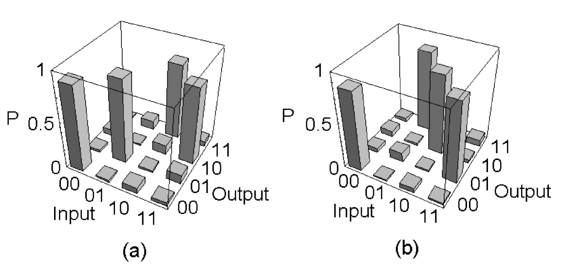
The measurement result of the input-output probabilities of our CNOT gate in the basis and in the basis are shown in tables 1(a) and 1(b), respectively. We measured the coincidence counts between two SPCMs by appropriately setting the HWPs for 16 different combinations of input and output states. In order to convert the coincidence rates to probabilities, we normalize them with the sum of coincidence counts obtained for the respective input state.
| (a) | ||||
|---|---|---|---|---|
| 0.898 | 0.031 | 0.061 | 0.011 | |
| 0.021 | 0.885 | 0.006 | 0.088 | |
| 0.064 | 0.027 | 0.099 | 0.810 | |
| 0.031 | 0.096 | 0.819 | 0.054 |
| (b) | ||||
|---|---|---|---|---|
| 0.854 | 0.044 | 0.063 | 0.039 | |
| 0.013 | 0.099 | 0.013 | 0.874 | |
| 0.050 | 0.021 | 0.871 | 0.058 | |
| 0.019 | 0.870 | 0.040 | 0.071 |
The three dimensional bar graphs of table 1 are shown in Fig. 3. The fidelity of the CNOT operation in the basis, defined as the probability of obtaining the correct output averaged over all four possible inputs, is . Similarly, the fidelity of the reverse CNOT operation in the basis is .
As discussed in detail in Hof04 , the two complementary fidelities and define an upper and lower bound for the quantum process fidelity of the gate with
| (1) |
Thus, our experimental results show that the process fidelity of our experimental quantum CNOT gate is
| (2) |
The lower bound of the process fidelity also defines a lower bound of the entanglement capability of the gate, since the fidelity of entanglement generation is at least equal to the process fidelity. In terms of the concurrence that the gate can generate from product state inputs, the minimal entanglement capability is therefore given by Hof04
| (3) |
Since our experimental results show that the minimal process fidelity of the gate is , the lower bound of the entanglement capability is
| (4) |
The experimental results shown in table 1 are therefore sufficient to confirm the entanglement capability of our gate.
In order to gain a better understanding of the noise effects in our experimental quantum gate, we can analyze the errors in the classical operations shown in table 1 and associate them with quantum errors represented by elements of the process matrix. For this purpose, it is useful to classify the errors according to the bit flip errors in the output of the operations in the and the basis, using 0 for the correct gate operation, C for a flip of the control bit output, T for a flip of the target bit output, and B for a flip of both outputs. It is then possible to expand the process matrix in terms of 16 orthogonal unitary operations , where the index 00, C0, B0, T0, 0C, CC, TC, BC, 0T, CT, TT, BT, 0B, CB, TB, BB defines the pair of error syndromes in the complementary operations in the and the basis, e.g. for a target flip error in the operation and a control flip error in the operation and for the ideal gate operation. The process matrix describing the noisy gate operation is given by the operator sum representation of the relation between an arbitrary input density matrix and its output density matrix ,
| (5) |
Since each operation describes a well defined combination of errors in the and operations, it is now possible to relate the error probabilities observed in table 1 to sums over the diagonal elements of the process matrix, as shown in table 2.
| X0 | XC | XT | XB | sum | |
|---|---|---|---|---|---|
| 0 X | |||||
| CX | |||||
| TX | |||||
| BX | |||||
| sum |
Since the correlations between errors in and errors in are unknown, a range of different distributions of diagonal elements is consistent with the experimental data. It is possible to illustrate this range of possibilities by considering the scenarios of lowest and highest process fidelity. The matrix elements of these cases are shown in tables 3(a) and 3(b).
| (a) | X0 | XC | XT | XB | sum |
|---|---|---|---|---|---|
| 0 X | |||||
| CX | |||||
| TX | |||||
| BX | |||||
| sum |
| (b) | X0 | XC | XT | XB | sum |
|---|---|---|---|---|---|
| 0 X | |||||
| CX | |||||
| TX | |||||
| BX | |||||
| sum |
In the worst case scenario of a process fidelity of shown in table 3(a), each error syndrome is only observed in either the or the basis. Therefore, the errors observed in the operation can be identified directly with C0,T0,B0, and the errors observed in the operation can be identified with 0C,0T,0B. In the optimal case of a process fidelity of shown in table 3(b), the diagonal elements of C0,T0,B0 for errors only in are all zero. The remaining errors have been distributed over the other diagonal matrix elements within the constraints given by table 2. Note that the distribution of matrix elements in the optimal case is far more homogeneous than the worst case scenario. The actual process fidelity is therefore likely to be closer to the upper limit of than to the lower limit of .
In conclusion, we have demonstrated the first experimental realization of an optical quantum CNOT gate without any path interference by measuring the fidelities of the classical CNOT operations in the computational basis and in the complementary basis. The performance of both operations by the same quantum gate at fidelities of and indicates that our device has a quantum process fidelity of and an entanglement capability of . Since the gate presented in this paper requires no path length adjustments, it should be ideal for the construction of quantum circuits using multiple gates. The present work may therefore provide an important first step towards the realization of optical quantum computation with larger numbers of qubits.
We would like to thank H. Fujiwara, K. Tsujino and D. Kawase for technical suggestions. This work was supported in part by Core Research for Evolutional Science and Technology, Japan Science and Technology Agency, Grant-in-Aid of Japan Science Promotion Society and 21st century COE program.
References
- (1) P.W. Shor, SIAM J. Comput. 26, 1484 (1997).
- (2) L.K. Grover, Phys. Rev. Lett. 79, 325 (1997).
- (3) G.J. Milburn, Phys. Rev. Lett. 62, 2124 (1989).
- (4) E. Knill, R. Laflamme and G.J. Milburn, Nature (London) 409, 46 (2001).
- (5) M. Koashi, T. Yamamoto, and N. Imoto, Phys. Rev. A 63, 030301(R) (2001).
- (6) T.B. Pittman, B.C. Jacobs, and J.D. Franson, Phys. Rev. A 64, 062311 (2001).
- (7) H.F. Hofmann, and S. Takeuchi, Phys. Rev. A 66, 024308 (2002).
- (8) T.C. Ralph, N.K. Langford, T.B. Bell, and A.G. White, Phys. Rev. A 65, 062324 (2002).
- (9) T.C. Ralph, A.G. White, W.J. Munro, and G.J. Milburn, Phys. Rev. A 65, 012314 (2002).
- (10) M.A. Nielsen, Phys. Rev. Lett. 93, 040503 (2004).
- (11) T.B. Pittman, B.C. Jacobs, and J.D. Franson, Phys. Rev. Lett. 88, 257902 (2002).
- (12) K. Sanaka, K. Kawahara, and T. Kuga, Phys. Rev. A 66, 040301(R) (2002).
- (13) T.B. Pittman, M.J. Fitch, B.C. Jacobs, and J.D. Franson, Phys. Rev. A 68, 032316 (2003).
- (14) J.L. O’Brien, G.J. Pryde, A.G. White, T.C. Ralph and D. Branning, Nature (London) 426, 264 (2003).
- (15) J.L. O’Brien, G.J. Pryde, A. Gilchrist, D.F.V. James, N.K. Langford, T.C. Ralph, and A.G. White, Phys. Rev. Lett. 93, 080502 (2004).
- (16) Z. Zhao, A. N. Zhang, Y. A. Chen, H. Zhang, J. F. Du, T. Yang, and J. W. Pan, Phys. Rev. Lett. 94, 030501 (2005).
- (17) H.F. Hofmann, Phys. Rev. Lett. 94, 160504 (2005).
- (18) S. Takeuchi, Opt. Lett. 26, 843 (2001).
- (19) C. Kurtsiefer, M. Oberparleiter, and H. Weinfurter, Phys. Rev. A 64, 023802 (2001).