Nanoscale atomic waveguides with suspended carbon nanotubes
Abstract
We propose an experimentally viable setup for the realization of one-dimensional ultracold atom gases in a nanoscale magnetic waveguide formed by single doubly-clamped suspended carbon nanotubes. We show that all common decoherence and atom loss mechanisms are small guaranteeing a stable operation of the trap. Since the extremely large current densities in carbon nanotubes are spatially homogeneous, our proposed architecture allows to create a very regular trapping potential for the atom cloud. Adding a second nanowire allows to create a double-well potential with a moderate tunneling barrier which is desired for tunneling and interference experiments with the advantage of tunneling distances being in the nanometer regime.
1 Introduction
The ongoing progress in the fabrication and manipulation of micro- or nanoscale structures has recently allowed for systematic studies of ultracold atom gases, where current-carrying wires and additional magnetic bias fields generate magnetic fields trapping neutral atoms (‘atom chips’) Folman02 ; Reichel02 . For instance, the Bose-Einstein condensation (BEC) of microchip-confined atoms has been successfully demonstrated by several groups atomBEC . So far, decoherence and atom loss constitute central impediments, since atoms are relatively close to ‘hot’ macroscopic surfaces or current-carrying wires (with typical diameters of several m), where the Casimir-Polder potential and Johnson noise can seriously affect stability Henkel99 ; chin ; Schroll03 . To reduce these effects, further miniaturization to the nanoscale regime would be desirable. In particular, this is promising in the context of integrated atomic matter-wave interferometry and optics Kasevich , and combines the strengths of nanotechnology and atomic physics. While at first sight this goal conflicts with the requirement of large currents forming tight trapping potentials, we propose that when using suspended carbon nanotubes (NTs) tubes (with diameters of a few nm) as wires, nanoscale atom chip devices with large current densities can be designed. In turn, these devices allow to trap ultracold atom gases basically free of trap-induced decoherence or atom losses, with the gas containing few tens of atoms. Since disorder is generally weak in NTs, the (extremely large) current density distribution is spatially homogeneous, which allows to overcome the problem of fragmentation of the atom cloud. Moreover, they can be built with state-of-the-art technology.
With relevant length scales below optical and cold-atom de Broglie wavelengths, this also paves the way for the observation of interesting and largely unexplored many-body physics in one dimension (1D) Petrov04 . Examples include the interference properties of interacting matter waves chen , the 1D analogue of the BEC-BCS crossover becbcs and shape resonances in 1D trapping potentials olshanii . Previous realizations of 1D cold atoms were reported using optical lattices esslinger ; Paredes04 ; Weiss and magnetic traps Goerlitz01 , but they involve arrays of 1D or elongated 3D systems, where it is difficult to separately manipulate a single 1D atom cloud (the distances between the 1D systems composing the array are few hundred nm). A noteworthy advantage of our proposal against dipole optical traps is that arrays of many NT waveguides can be built, where it is possible to manipulate an individual trap by changing the current through an individual NT. Moreover, our proposal allows to minimize unwanted substrate effects and implies a drastically reduced transverse size (a few nm) of the cloud. We expect that our approach allows to observe new interesting many-body features not accessible by the otherwise very successful atom chip setup. This could provide a fruitful link between atomic and condensed matter physics with a wealth of fascinating effects.
2 The setup
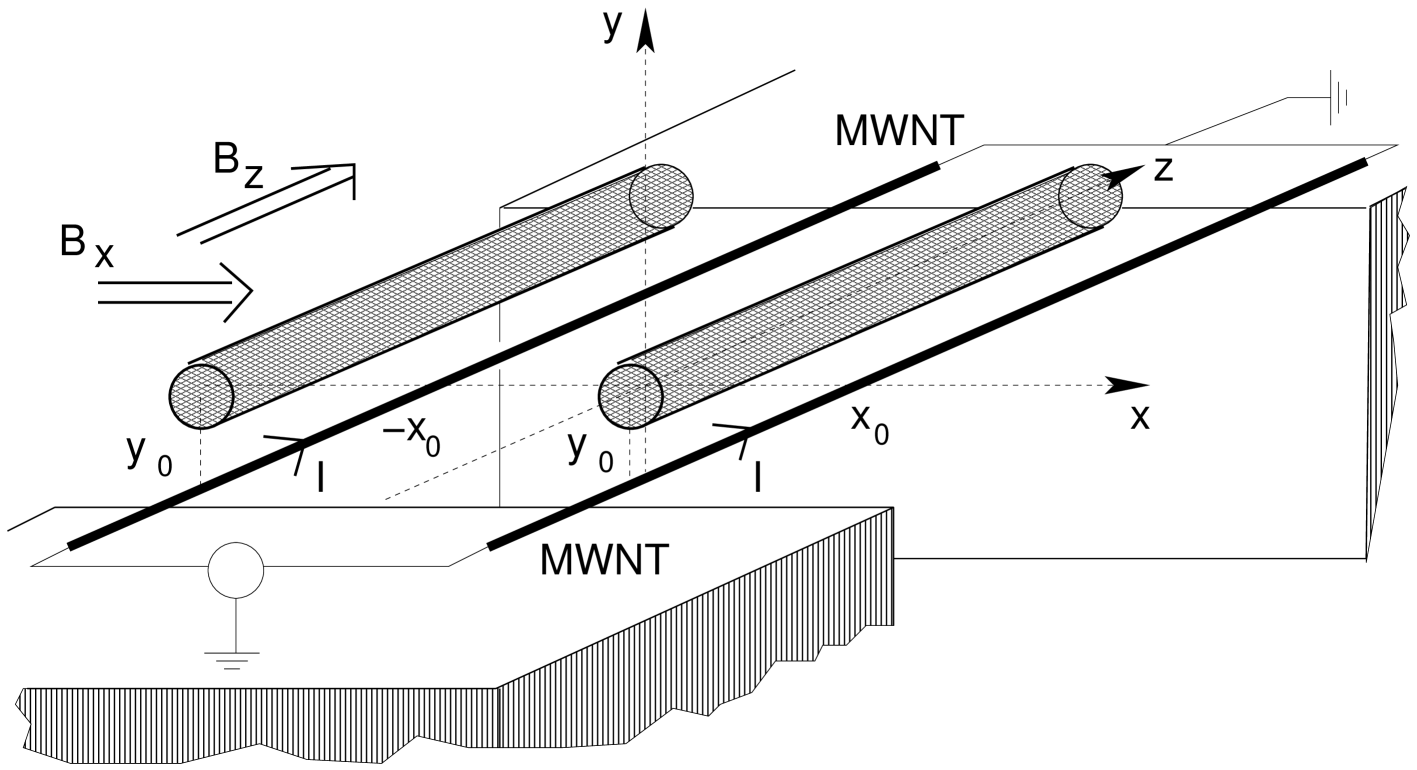
A typical proposed nanoscale waveguide setup to confine ultracold atoms to 1D is sketched in Fig. 1. The setup employs a single suspended doubly-clamped NT (left NT in Fig. 1, the second suspended NT on the right will be used to create a double-well potential, see below), where nanofabrication techniques routinely allow for trenches with typical depths and lengths of several m tubes . To minimize decoherence and loss effects chin , the substrate should be insulating apart from thin metal strips to electrically contact the NTs. Since strong currents (hundreds of A) are necessary, thick multiwall nanotubes (MWNTs) or ‘ropes’ tubes are best suited. The suspended geometry largely eliminates the influence of the substrate. A transverse magnetic field is required to create a stable trap while a longitudinal magnetic field suppresses Majorana spin flips sukumar ; jones . With this single-tube setup, neutral atoms in a weak-field seeking state can be trapped. Studying various sources for decoherence, heating or atom loss, and estimating the related time scales, we find that, for reasonable parameters, detrimental effects are small. As a concrete example, we shall consider 87Rb atoms in the weak-field seeking hyperfine state .
We next describe the setup in Fig. 1, where the (homogeneous) current flows through the left NT positioned at . With regard to the decoherence properties of the proposed trap, it is advantageous that the current flows homogeneously through the NT, as disorder effects are usually weak in NTs tubes . Neglecting boundary effects due to the finite tube length , the magnetic field at is given by
| (1) |
with the vacuum permeability . To create a trapping potential minimum at , the transverse magnetic field is . Then the transverse confinement potential is , where with the Landé factor and the Bohr magneton . It has a minimum along the line , with the distance between the atom cloud and the wire being . Under the adiabatic approximation sukumar , is a constant of motion, and the potential is harmonic very close to the minimum of the trap, i.e., , with frequency and associated transverse confinement length , where is the atom mass. The adiabatic approximation is valid as long as with the Larmor frequency . Non-adiabatic Majorana spin flips to a strong-field seeking state generate atom loss Folman02 ; jones characterized by the rate , with sukumar . For convenience, we switch to a dimensionless form of the full potential by measuring energies in units of and lengths in units of ,
| (2) |
which depends only on and . The trap frequency then follows as
| (3) |
Note that a real trap also requires a longitudinal confining potential with frequency .
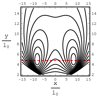
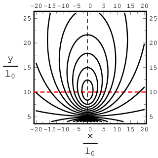
To obtain an estimate for the design of the nanotrap, we choose realistic parameters: , corresponding to a rate of spin flip transition per oscillation period . Decreasing increases the trap frequency. However, cannot be chosen too small, for otherwise the potential is not confining anymore (and the harmonic approximation becomes invalid). Using for the potential at , we now show that for , the harmonic approximation breaks down. To see this, note that for , the potential provides a confining barrier (in units of the trap frequency ) of , while for , we get only . Thus exceedingly small values of would lead to unwanted thermal atom escape processes out of the trap. To illustrate the feasibility of the proposed trap design, we show in Table 1 several parameter combinations with realistic values for the MWNT current together with the resulting trap parameters. In practice, first the maximum possible current should be applied to the NT, with some initial field . After loading of the trap, the field should be increased, the cloud thereby approaching the wire with a steepening of the confinement. At the same time, and consequently decrease. This procedure can be used to load the nanotrap from a larger magnetic trap (ensuring mode matching). For a given current, there is a corresponding lower limit for stable values of from the requirement , as already mentioned above. To give an example, the confining potential is shown in Fig. 2a) for A, representing a reasonable current through thick NTs tubes , , and (where ). The resulting trap frequency is kHz and the associated transverse magnetic field is G.
3 Influence of destructive effects
For stable operation, it is essential that destructive effects like atom loss, heating or decoherence are small.
(i) One loss process is generated by non-adiabatic Majorana spin flips as discussed above.
(ii) Atom loss may also originate from noise-induced spin flips, where current fluctuations cause a fluctuating magnetic field generating the Majorana spin flip rate Henkel99
| (4) |
At room temperature and for typical voltages V, we have , and is expected to equal the shot noise of a diffusive wire. For the parameters above, a rather small escape rate results, Hz. If a (proximity-induced) supercurrent is applied to the MWNT, the resulting current fluctuations could be reduced even further.
(iii) Thermal NT vibrations might create decoherence and heating, and could even cause a transition to the first excited state of the trap. Using a standard elasticity model for a doubly clamped wire in the limit of small deflections, the maximum mean square displacement is Sapmaz03
where is the NT displacement, the (suspended) NT length, the temperature, the Young modulus, and the NT’s moment of inertia. For m and typical material parameters from Ref. tubes , we find nm at room temperature. This is much smaller than the transverse size of the atomic cloud. Small fluctuations of the trap center could cause transitions to excited transverse trap states. Detailed analysis shows that the related decoherence rate is also negligible, since the transverse fundamental vibration mode of the NT has the frequency
| (5) |
with , the mass density , and the cross-sectional area . For the above parameters, MHz is much larger than the trap frequency itself. Due to the strong frequency mismatch, the coupling of the atom gas to the NT vibrations is therefore negligible.
(iv) Another decoherence mechanism comes from current fluctuations in the NTs. Following the analysis of Ref. Schroll03 , the corresponding decoherence rate is
| (6) |
where is the NT conductivity and the cross-sectional area through which the current runs in the NT. For the corresponding parameters we find .
(v) Another potential source of atom loss could be the attractive Casimir-Polder force between the atoms and the NT surface. The Casimir-Polder interaction potential between an infinite plane and a neutral atom is given by chin ; Casimir48 . For a metallic surface and 87Rb atoms, Jm4, implying that at a distance of m from the surface, the characteristic frequency associated with the Casimir-Polder interaction is kHz. In our setup, however, we cannot apply this estimate since the assumption of an infinite plane is not realistic for a NT with a diameter of a few tens of nm. Instead, we expect that the distance between the cloud and the NT can be reduced without drastically increasing the Casimir-Polder force. The proposed setup could be an interesting playground to study the Casimir-Polder interaction for our more complicated geometry.
(vi) A further possible mechanism modifying the shape of the confining potential is the influence of the electric field between the two contacts of the nanowire and the macroscopic leads which is created by the transport voltage. This field depends strongly on the detailed geometry of the contacts. However, the electric field can in general be reduced if the total length of the NT is increased. (Note that can be different from the length over which the NT is suspended). Due to the small intrinsic NT resistivity, the influence of the contact resistance then decreases for longer NTs. Finally, we mention that superconducting leads could be used to reduce the voltage drop.
4 Number of trapped atoms and size of atom cloud
Next we address the important issue of how many atoms can be loaded into such a nanotrap. This question strongly depends on the underlying many-body physics which determines for instance the density profile of the atom cloud. Since the trap frequencies given in Table 1 exceed typical thermal energies of the cloud, we will consider the 1D situation. Within the framework of two-particle s-wave scattering in a parabolic trap, the effective 1D interaction strength is related to the 3D scattering length according to olshanii
| (7) |
where Interestingly, shows a confinement-induced resonance (CIR) for olshanii . For nearly parabolic traps respecting parity symmetry, this CIR is split into three resonances Peano . However, for the typical trap frequencies displayed in Table 1, corresponding to non-resonant atom-atom scattering, the parabolic confinement represents a very good approximation. For free bosons in 1D, the full many-body problem can be solved analytically Lieb . It turns out that the governing parameter is given by , where is the atom density in the cloud. For weak interactions (large ), a Thomas-Fermi (TF) gas results, while in the opposite regime, the Tonks-Girardeau (TG) gas is obtained.
For realistic traps with an additional longitudinal confining potential with frequency , the problem has been addressed in Ref. Dunjko . The corresponding governing parameter is where is the cloud density in the center of the trap in the TF approximation. Small characterizes a TG gas whereas large corresponds to the TF gas. The longitudinal size of the atom cloud in terms of the atom number and the longitudinal (transversal) trap frequencies () has been computed in Ref. Dunjko , with the result
| (8) |
in the TF regime and
| (9) |
in the TG regime. In order to determine the cloud size , we first calculate for fixed and , and then use the respective formula Eq. (8) or (9). In the crossover region, both expressions yield similar results that also match the full numerical solution Dunjko . Typical results for realistic parameters are listed in Table 2 for kHz. From these results, we conclude that the length of the suspended NT should be in the m-regime in order to trap a few tens of 87Rb atoms.
To summarize the discussion of the monostable trap, we emphasize that the proposed nanotrap is realistic, with currents of a few 100 A and lengths of few m of the suspended parts of NT. No serious fundamental decoherence, heating or loss mechanisms are expected for reasonable parameters of this nanotrap. We note that we did not consider additional specific noise sources from further experimental equipment.
5 Double-well potential with two carbon nanotubes
In order to illustrate the advantages of the miniaturization to the nanoscale, let us consider a setup which allows two stable minima separated by a tunneling barrier. The simplest setup consists of two parallel NTs carrying co-propagating currents , a (small) longitudinal bias field and a transverse bias field . Such a double-well potential for 1D ultracold atom gases would permit a rich variety of possible applications. Experiments to study Macroscopic Quantum Tunneling and Macroscopic Quantum Coherence phenomena weiss between strongly correlated 1D quantum gases could then be performed. In addition, qubits forming the building blocks for a quantum information processor could be realized. The rich tunability of the potential shape, including tuning the height of the potential barrier as well as the tunneling distance, is a particularly promising feature.
To realize this potential, we propose to place a second current-carrying NT at , where the condition guarantees the existence of two minima located at . By tuning the transversal magnetic field and the current , and thus the location of the minima can be modified. Around these minima, the potential is parabolic with frequency
| (10) |
Similar to the considerations above, we obtain the potential in units of , which depends only on , and ,
Figure 2b) shows the corresponding bistable potential for the particular case of , A, nm and nm. The two minima are clearly discerned. To see how the frequency in the single well develops if the current in the second wire is turned on, we introduce the reference frequency in the single-well case with a fixed current and a fixed transverse field , such that . Then we obtain the ratio
| (12) |
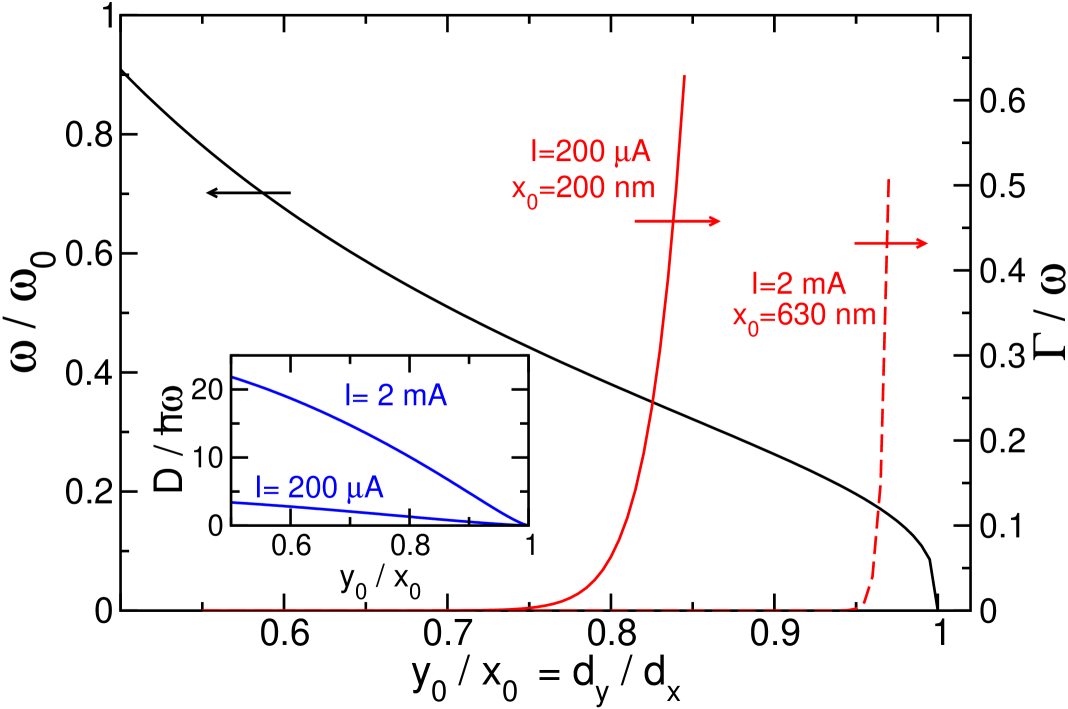
For decreasing and keeping constant, we find that decreases as shown in Fig. 3 (black solid line and left scale), while the distance of the atom cloud increases. In the limit , the two minima merge and the potential becomes quartic and monostable, implying that . For the above parameter set, we find kHz. Since one could obtain the same for a larger current and a correspondingly larger distance , one gets the same trap frequency for a fixed ratio of . However, and themselves would change and since the parabolic frequency is fixed, only the non-linear corrections to the parabolic potential will be modified. This in turn influences the height of the potential barrier and the tunneling rate between the two wells. Next we study the influence of the length scale on these two quantities.
Taking the full potential into account, we estimate the barrier height and the tunneling rate within a simple single-particle WKB approximation. The barrier height separating the two stable wells,
| (13) |
is shown as a function of for two values of in the inset of Fig. 3. Note that the barrier height is of the order of a few multiples of the energy gap in the wells, implying that the potential is in the deep quantum regime, favoring quantum-mechanical tunneling between the two wells. The corresponding tunneling rate for the lowest-lying pair of energy eigenstates follows in WKB approximation as
| (14) |
where are the (dimensionless) classical turning points in the inverted potential at energy , which is approximately the ground-state energy of a single well. The integral in Eq. (14) is calculated along the line connecting the two minima corresponding to . Results for are shown in Fig. 3 (red solid lines and right scale) as a function of for two different values of the current and the distance yielding the same . Note that for the smaller current, A, assumes large values already for large frequencies . This also implies that the detrimental effects discussed above are less efficient. On the other hand, for large currents, the tunneling regime is entered only for much smaller trap frequencies. For the above parameters, we find kHz. For the smaller current, the tunneling regime starts at frequencies of around kHz, corresponding to a temperature of K, while for the larger current, the tunneling regime is entered at kHz corresponding to K. This behaviour illustrates qualitatively (in the single-particle picture) one of the benefits of miniaturization. We believe that the features also appear in a more detailed consideration involving the atomic correlations which is not pursued here.
A potential drawback of the double wire configuration could be the transverse NT deflection due to their mutual magnetic repulsion. For an estimate, note that the NT displacement field obeys the equation of motion . The static solution under the boundary conditions is . Using again parameters from Ref. tubes , we find the maximum displacement nm for m. Hence the mutual magnetic repulsion of the NTs is very weak. Finally, we note that a potential misalignment of the two NT wires is no serious impediment for the design. Experimentally available techniques could be combined which allow on the one hand to move a NT on a substrate by an atomic force microscope Henk00 , while on the other hand, the NTs can be suspended and contacted after being positioned Kim02 .
6 Conclusions
To conclude, we propose a nanoscale waveguide for ultracold atoms based on doubly clamped suspended nanotubes. We have analyzed this scenario from an atom chip point of view. All common sources of imperfection can be made sufficiently small to enable stable operation of the setup. Two suspended NTs can be combined to create a bistable potential in the deep quantum regime. When compared to conventional atom-chip traps employed in present experiments, such nanotraps offer several new and exciting perspectives that hopefully motivate experimentalists to realize this proposal. More refined models to study the interplay between the mechanical motion of the NTs and the coherent dynamics of the atom cloud are imaginable and could establish a link between the field of nanoelectromechanical systems and cold atom physics.
First, rather large trap frequencies can be achieved while at the same time using smaller wire currents. This becomes possible here because both the spatial size of the atom cloud and its distance to the current-carrying wire(s) would be reduced to the nanometer scale, and because NTs allow typical current densities of Anm2, which should be compared to the corresponding densities of nAnm2 in noble metals. For the case of a single-well trap, the resulting trap frequencies go beyond realized chip traps Folman02 . Large trap frequencies at low currents are generally desirable, since detrimental effects like decoherence, Majorana spin flips, or atom loss will then be significantly reduced. Moreover, the faster dynamics of the atoms could lead to the construction of fast ”chip circuits”.
Second, regarding our proposal of a bistable potential with strong tunneling, the miniaturization towards the nanoscale represents a novel opportunity to study coherent and incoherent tunneling of a macroscopic number of cold atoms. The proposed bistable nanotrap is characterized by considerably reduced tunneling distances, thus allowing for large tunneling rates at large trap frequencies. Note that the energy scale associated with tunneling is larger than thermal energies for realistic temperatures. Such a bistable device could then switch between the two stable states on very short time scales enabling the design of fast switches. Within our proposal the parameters of the bistable potential can be tuned over a wide range by modifying experimentally accessible quantities like the current or magnetic fields.
A third advantage of this proposal results from the homogeneity of the currents flowing through the NTs. As NTs are characterized by long mean free paths, they often constitute (quasi-)ballistic conductors, where extremely large yet homogeneous current densities are possible which avoids the fragmentation problem Folman02 .
Detection certainly constitutes an experimental challenge in this truly 1D limit. However, we note that single-atom detection schemes are currently being developed, which would also allow to probe the tight 1D cloud here, e.g., by combining cavity quantum electrodynamics with chip technology Reichel02 , or by using additional perpendicular wires/tubes ‘partitioning’ the atom cloud reichel . This may then allow to study interesting many-body physics in 1D in an unprecedented manner.
7 Acknowledgments
We thank A. Görlitz, Y. Kobayashi, C. Mora, H. Postma, and J. Schmiedmayer for fruitful discussions. V. P. and M. T. would like to thank H. Takayanagi and K. Semba for the kind hospitality at the NTT Basic Research Laboratories, where parts of this work have been accomplished. We acknowledge support by the DFG-SFB TR-12 and by the Japanese CREST/JST.
References
- (1) R. Folman, P. Krüger, J. Schmiedmayer, J. Denschlag, and C. Henkel, Adv. At. Mol. Opt. Phys. 48, 263 (2002)
- (2) J. Reichel, Appl. Phys. B 75, 469 (2002)
- (3) H. Ott, J. Fortagh, G. Schlotterbeck, A. Grossmann, and C. Zimmermann, Phys. Rev. Lett. 87, 230401 (2001); W. Hänsel, P. Hommelhoff, T.W. Hänsch, and J. Reichel, Nature 413, 498 (2001); A. Leanhardt, Y. Shin, A. P. Chikkatur, D. Kielpinski, W. Ketterle, and D. E. Pritchard, Phys. Rev. Lett. 90, 100404 (2003); S. Schneider, A. Kasper, Ch. vom Hagen, M. Bartenstein, B. Engeser, T. Schumm, I. Bar-Joseph, R. Folman, L. Feenstra, and J. Schmiedmayer, Phys. Rev. A 67, 023612 (2003)
- (4) C. Henkel, S. Pötting, and M. Wilkens, Appl. Phys. B 69, 379 (1999)
- (5) Yu-ju Lin, I. Teper, C. Chin, and V. Vuletić, Phys. Rev. Lett. 92, 050404 (2004)
- (6) C. Schroll, W. Belzig, and C. Bruder, Phys. Rev. A 68, 043618 (2003)
- (7) M.A. Kasevich, Science 298, 136 (2002)
- (8) M.S. Dresselhaus, G. Dresselhaus, and Ph. Avouris (eds.), Carbon Nanotubes (Berlin, Springer 2001)
- (9) D.S. Petrov, D.M. Gangardt, and G.V. Shlyapnikov, J. Phys. IV France 116, 5 (2004)
- (10) S. Chen and R. Egger, Phys. Rev. A 68, 063605 (2003).
- (11) I.V. Tokatly, Phys. Rev. Lett. 93, 090405 (2004); J.N. Fuchs, A. Recati, and W. Zwerger, ibid. 93, 090408 (2004); C. Mora, R. Egger, A.O. Gogolin, and A. Komnik, ibid. 93, 170403 (2004)
- (12) M. Olshanii, Phys. Rev. Lett. 81, 938 (1998); T. Bergeman, M.G. Moore, and M. Olshanii, ibid. 91, 163201 (2003)
- (13) T. Stöferle, H. Moritz, C. Schori, M. Köhl, and T. Esslinger, Phys. Rev. Lett. 92, 130403 (2004)
- (14) B. Paredes, A. Widera, V. Murg, O. Mandel, S. Fölling, I. Cirac, G. V. Shlyapnikov, T. W. H nsch, and I. Bloch, Nature 429, 277 (2004)
- (15) T. Kinoshita, T. Wenger, and D.S. Weiss, Science 305, 112 (2004)
- (16) A. Görlitz, J. M. Vogels, A. E. Leanhardt, C. Raman, T. L. Gustavson, J. R. Abo-Shaeer, A. P. Chikkatur, S. Gupta, S. Inouye, T. Rosenband, and W. Ketterle, Phys. Rev. Lett. 87, 130402 (2001)
- (17) C.V. Sukumar and D.M. Brink, Phys. Rev. A 56, 2451 (1997)
- (18) M. P. A. Jones, C. J. Vale, D. Sahagun, B. V. Hall, and E.A. Hinds, Phys. Rev. Lett. 91, 080401 (2003)
- (19) S. Sapmaz, Ya.M. Blanter, L. Gurevich, and H.S.J. van der Zant, Phys. Rev. B 67, 235414 (2003)
- (20) H. B. G. Casimir and D. Polder, Phys. Rev. 73, 360 (1948)
- (21) V. Peano, M. Thorwart, C. Mora, and R. Egger, unpublished results, see also cond-mat/0411517
- (22) E. H. Lieb, W. Liniger, Phys. Rev. 130, 1616 (1963)
- (23) V. Dunjko, V. Lorent, and M. Olshanii, Phys. Rev. Lett. 86, 5413 (2001)
- (24) U. Weiss, Quantum Dissipative Systems (World Scientific, Singapore, 1999)
- (25) H. W. Ch. Postma, A. Sellmeijer, and C. Dekker, Adv. Mater. 17, 1299 (2000)
- (26) G.-T. Kim, G. Gu, U. Waizman, and S. Roth, Appl. Phys. Lett. 80, 1815 (2002)
- (27) J. Reichel and J.H. Thywissen, J. Phys. IV France 116, 265 (2004)
| 1000 | 10 | 2460 | 144 | 14 |
| 250 | 5 | 2460 | 72 | 14 |
| 250 | 10 | 228.7 | 576 | 58 |
| 100 | 5 | 273.8 | 180 | 36 |
| 100 | 10 | 24.6 | 1440 | 144 |
| 50 | 5 | 218.4 | 360 | 72 |
| 25 | 5 | 24.6 | 720 | 144 |
| N | ||||
|---|---|---|---|---|
| 2460 | -26.65 | 30 | 0.11 | 7.7 |
| 2460 | -26.65 | 50 | 0.15 | 10 |
| 273.8 | -223 | 30 | 0.67 | 7.3 |
| 273.8 | -223 | 50 | 0.94 | 8.7 |
| 273.8 | -223 | 100 | 1.49 | 11 |
| 228.76 | -603 | 30 | 2.55 | 5.3 |
| 228.76 | -603 | 50 | 3.58 | 6.3 |
| 228.76 | -603 | 100 | 5.72 | 7.9 |
a1)
 b1)
b1)

a2)
 b2)
b2)