Atomic spin decoherence near conducting and superconducting films
Abstract
We derive scaling laws for the spin decoherence of neutral atoms trapped near conducting and superconducting plane surfaces. A new result for thin films sheds light on the measurement of Y.J. Lin, I. Teper, C. Chin, and V. Vuletić [Phys. Rev. Lett. 92, 050404 (2004)]. Our calculation is based on a quantum-theoretical treatment of electromagnetic radiation near metallic bodies [P.K. Rekdal, S. Scheel, P.L. Knight, and E.A. Hinds, Phys. Rev. A 70, 013811 (2004)]. We show that there is a critical atom-surface distance that maximizes the spin relaxation rate and we show how this depends on the skin depth and thickness of the metal surface. In the light of this impedance-matching effect we discuss the spin relaxation to be expected above a thin superconducting niobium layer.
pacs:
42.50.Ct, 34.50.Dy, 03.75.BeTrapped neutral atoms have intrinsically long coherence times, making them suitable for many proposed applications based on quantum state manipulation. These include interferometry interferometry , low-dimensional quantum gas studies quantum gas , and quantum information processing Jaksch ; Calarco ; proposals . The trapping structures required for these applications typically have feature sizes on the micron or sub-micron scale, sizes that are comparable with the atomic de Broglie wavelength. The required trap frequencies are typically in the 1 kHz to 1 MHz range, this being energetic enough to compete with the temperature and chemical potential and to allow adiabatic manipulation on the sub-ms timescale. One way to achieve these requirements is with intensity gradients of light, which make neutral atom traps by virtue of the optical dipole force. Major progress has been made with this approach Bloch ; Esslinger ; Phillips ; Ketterleinterferometer , but still, the light is not arbitrarily configurable and it is difficult to address specific sites of an optical lattice. Structures microfabricated on a surface, known as atom chips, are emerging as a very promising alternative Hindsreview ; Schmiedmayerreview . These can be patterned in complex arrays on micrometer length scales. The locally-addressed electric, magnetic and optical fields on a chip provide great flexibility for manipulating and addressing the atoms. Magnetic traps on atom chips are commonly generated either by microfabricated current-carrying wires Schmiedmayerreview or by poled ferromagnetic films Hindsreview ; Eriksson attached to some dielectric or metallic substrate. These are used to create local minima of the magnetic field strength in which low-field-seeking alkali atoms are trapped by the Zeeman effect.
In order to utilize atom chip structures of small scale, the atoms must be held close to the surface. However, this same proximity threatens to decohere the quantum state of the atoms through electromagnetic field fluctuations that occur in the vicinity of a surface. The free photon field does not perturb ground state alkali atoms appreciably, but the evanescent field modes associated with surface currents can be dense enough to generate significant rf noise. This effect arises because the resistivity of the surface material is always accompanied by field fluctuations as a consequence of the fluctuation-dissipation theorem. Several experimental studies have recently shown that rf spin flip transitions occur when atoms are held close to thick metallic or dielectric surfaces Jones ; Cornell ; Vuletic . Comparison with theory Henkel ; Rekdal has shown that this spin relaxation is indeed due to thermal fluctuations of the surface modes.
In this article, we explore the possibilities for reducing the spin decoherence due to surface fields by making metallic surfaces thin and by the possible use of superconducting materials. Previous studies have found valuable scaling laws for the lifetime near thick metallic slabs Henkel and multi-layer wires Rekdal . The new results we derive here are of interest because they describe the current generation of atom chips using thin films and can guide future designs to achieve long qubit coherence times.
Consider a ground-state alkali atom in hyperfine magnetic state and trapped at position near a surface. The rate of the magnetic spin flip transition to state has been derived by Rekdal et al. Rekdal as
| (1) | |||||
Here is the Bohr magneton, is the electron spin -factor and is the matrix element of the electron spin operator corresponding to the transition . Thermal excitations of the electromagnetic field modes are accounted for by the factor , where
| (2) |
is the mean number of thermal photons per mode at the frequency of the spin flip. The dyadic Green tensor is the unique solution to the Helmholtz equation
| (3) |
U being the unit dyad. This tensor contains all relevant information about the geometry of the set-up and also, through the dielectric permittivity , about the electric properties of the surface. Equation (1) follows from a consistent quantum-mechanical treatment of electromagnetic radiation in the presence of absorbing bodies (for a review, see Buch ). It is obtained by by considering the Heisenberg equations of motion for a quantized magnetic dipole in the rotating-wave and Markov approximations. The result is similar to calculations using Fermi’s Golden Rule Henkel , where the local density of states plays the rôle of the imaginary part of .
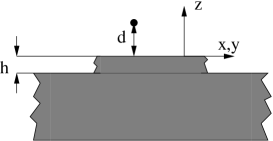
The geometry we are considering is illustrated in Fig. 1. We assume that a metallic slab of thickness extends to infinity in the and directions (this is solely for the computational simplicity that follows from translational invariance in two directions). There is a thick non-metallic substrate below and a vacuum above, where the atom is located at a distance from the surface of the metal. Our choice of -axis corresponds to having a bias magnetic field parallel to the surface, as is normally the case for a Ioffe-Pritchard trap above an atom chip. The Green function for this 3-layer structure, which is needed in order to use Eq. (1), is commonly expressed in terms of a series of cylindrical vector wave functions with appropriately chosen generalized (Fresnel) reflection coefficientsgreen . There are straightforward numerical routines that compute the required elements of the Green tensor.
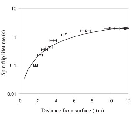
Recent experiments measuring spin flip relaxation rates of atoms trapped near thick surfaces have demonstrated the importance of thermal field fluctuations Jones ; Cornell ; Vuletic . This has promoted great interest in thin surfaces because they should generate less thermal noise, a conjecture that we confirm here. A recent publication Vuletic gives experimental values for the loss rate of 87Rb atoms in the state, magnetically trapped near a thin surface. The surface was a m-thick copper layer on a substrate of nitride-coated silicon. The data points shown in Fig. 2 reproduce the lifetimes for loss of atoms from the trap in Vuletic . At distances greater than about 7 m from the surface, the loss rate is essentially constant and is due to collisions with the background gas. At shorter distances, the lifetime is reduced by thermally-induced spin relaxation. Seeking a comparison with theory, the authors interpolated scaling laws given in Henkel and found agreement between theory and experiment for distances down to m. Below that, there seemed to be a discrepancy, with the observed lifetimes being substantially shorter than expected. It was surmised that this discrepancy might be due to patch potentials on the surface.
In the hope of resolving the discrepancy, we have calculated the lifetimes from Eq. (1). This was done numerically, using the Green’s function technique discussed above. Our result is shown as the solid line in Fig. 2. For the permittivity of the substrate, we ignored the silicon nitride and took corresponding to the silicon, but the result is not appreciably different even for because the permittivity of the metal layer () is so high that the Fresnel coefficients are not sensitive to such detail. At the greatest distances in Fig. 2 there is just the residual gas lifetime given by the authors of the experiment. Below m, our calculation gives a slightly low lifetime because the metal surface in the experiment was only m wide, rather than being infinitely wide as our calculation supposes. At lower heights still, where infinite width is a good approximation, we again see agreement with the experiment. This result indicates that the measurements in ref.Vuletic were correct and there is no need to invoke a possible contamination of the surface.
The spin flip lifetime for the transition depends on three independent length scales: the substrate thickness , the atom-surface distance , and the skin depth of the substrate material, defined via the Drude relation Jackson . For certain regimes of these parameters it is possible to approximate the integrals involved to obtain analytical results for the lifetime . Our results are
| (4) |
Here, is the lifetime in free space at zero temperature, given by . At a transition frequency of kHz this has the value s. At a temperature of K, the factor reduces the free-space lifetime to s, but this is still very long, being approximately the age of the universe. The remaining factors take into account the effect of the surface and these lead to much more dramatic reductions in lifetime. The first two results in Eq. (4) describe the case of a thick slab and are already known from ref. Henkel . The third result is new and describes the case of a thin film, which is the case for most atom chips in use today.
In order to illustrate some aspects of these results, Fig. 3 shows the spin-flip lifetime versus the skin depth of the metal film for the same Rb transition in an atom placed m away from the surface. The two curves correspond to an infinitely thick film (solid line) and to a m-thick film (dotted).

Where the skin depth is less than m, the two cases are effectively the same because the source of the noise lies within approximately one skin depth of the surface. Here the lifetime scales as in accordance with the first line of Eq. (4). As the skin depth becomes longer we enter a range where for the thin film. Here the thin film produces a shorter lifetime than the thick one, somewhat surprisingly. Once becomes large compared with , the case of the thick film is described by the second line of Eq. (4) whereas that of the thin film follows the third line. In either case , as can be seen on the right side of Fig. 3, with the important difference that the thin film gives a longer lifetime by a factor of .
Between the large and small extremes of skin depth the lifetime exhibits a minimum (see also Rekdal ). For thick films, we find the minimum at , whereas for thin films it is at . Evidently the minimum represents a condition for coupling the excitation most efficiently out of the atom and into surface excitations - a kind of impedance matching. One consequence of the minimum is that for any fixed atom-surface distance , there are two possible choices for the skin depth of the metallic film to produce a given lifetime. For example, with the atom placed m above a thick slab, Fig. 3 shows that skin depths of m and m both lead to a s lifetime. At the kHz frequency used for this figure, the larger skin depth corresponds to a slab of metal such as Cu (m) or Al (m), both excellent conductors.
There are of course no normal metals with a skin depth at kHz as small as m (a resistivity of m), but superconductors are possible candidates. In a material with superconducting gap at temperature , the usual Maxwell-Boltzmann distribution determines the fraction of Cooper pairs that are thermally broken to form a gas of normally conducting electrons Tinkham . Typically , where is the transition temperature. Thus, at temperatures that are moderately below there is a significant fraction of normally-conducting electrons. On the other hand, when , this fraction becomes vanishingly small.
One particularly relevant superconducting material for possible use in atom chips is niobium, because it has a high transition temperature. In bulk material K Klein , while K has been measured for films with nm thickness Pronin . The superconducting energy gap is estimated to be Pronin . Measurements of the complex magnetic susceptibility of ultra-pure niobium (residual resistivity ratio ) have recently been published in Casalbuoni . These are of particular interest here because they provide explicit figures for the real part of the complex conductivity at frequencies MHz. Just above the superconducting transition temperature the conductivity is Casalbuoni , which, through the relation , gives a skin depth in the normal state at kHz of m. The magnetic susceptibility measurements of Casalbuoni show a hundredfold increase in conductivity when the temperature drops to K, corresponding to a skin depth of m. This is significantly larger than the zero-temperature London penetration depth of nm Casalbuoni .
This analysis shows that i) superconducting films have the potential to provide surfaces with skin depths of 1 micron or less. ii) that the atom-surface distances similar in magnitude to the skin depth are to be avoided. For atom chips with the atoms at tens of microns away from the surface, the use of superconducting niobium wires at 4K can boost the spin relaxation time to s. This boost comes partly from the lower temperature which accounts for a 100 times smaller value of . This enhancement would be present for normal metals as well. From Fig. 3 we also see that part of this boost comes from the smaller skin depth of superconductors. However, small scale trapping structures are required for many quantum information processing schemes (e.g. Calarco ), and then it is natural to hold the atoms one or two microns away from the surface. In these cases, the unfortunate similarity between the atom-surface distance and the skin depth can make a superconducting surface a worse choice than a normal metal.
In conclusion, we have used a consistent quantum-theoretical description of electromagnetic radiation near metallic/dielectric bodies to derive an expression for the spin relaxation lifetime of a neutral atom held near the thin plane metallic surface of an atom chip. We have been able to show that the lifetime reported near such an atom chip by the group of Vuletić Vuletic is consistent with this theory. We have found that the spin-relaxation lifetime of an atom trapped at a given height above a metallic surface exhibits a minimum with respect to the skin depth of the surface. For atoms placed tens or hundreds of microns away from the surface, superconducting atom chips at low temperature offer improved lifetimes. However, we find that when atoms are placed only a few microns from the surface, as in many current atom chip experiments, the spin relaxation above normal metals is liable to be slower than above a superconductor. These results will be helpful in guiding the design of future miniaturized atom chips.
We acknowledge valuable discussions with D. Lee. This work was supported by the UK Engineering and Physical Sciences Research Council (EPSRC) and the European Commission (FASTnet and QGATES programmes). P.K.R. acknowledges support by the Research Council of Norway. S.S. enjoys the support of the EPSRC through an Advanced Research Fellowship.
References
- (1) E.A. Hinds, C.J. Vale, and M.G. Boshier, Phys. Rev. Lett. 86, 1462 (2001); W. Hänsel, P. Hommelhoff, T.W. Hänsch, and J. Reichel, Phys. Rev. A 64, 063607 (2001).
- (2) Journal de Physique IV 116, ‘Quantum Gases in Low Dimensions 2003’ eds. L. Pricoupenko, H. Perrin, and M. Olshnii (EDP Sciences, France 2004).
- (3) D. Jaksch, C. Bruder, J.I. Cirac, C.W. Gardiner, and P. Zoller, Phys. Rev. Lett. 81, 3108 (1998).
- (4) T. Calarco, E.A. Hinds, D. Jaksch, J. Schmiedmayer, J.I. Cirac, and P. Zoller, Phys. Rev. A 61, 022304 (2000); D. Jaksch, Contemp. Phys. 45, 367 (2004).
- (5) U. Dorner, P. Fedichev, D. Jaksch, M. Lewenstein, and P. Zoller, Phys. Rev. Lett. 91, 073601 (2003); J.K. Pachos and P.L. Knight, Phys. Rev. Lett. 91, 107902 (2003).
- (6) M. Greiner, O. Mandel, T. Esslinger, T.W. Hänsch, and I. Bloch Nature (London) 415, 39 (2002); O. Mandel, M. Greiner, A. Widera, T. Rom, T.W. Hänsch, and I. Bloch, Nature (London) 425, 937 (2003).
- (7) H. Moritz, T. Stöferle, M. Köhl, and T. Esslinger, Phys. Rev. Lett. 91, 250402 (2003).
- (8) S. Peil, J.V. Porto, B. Laburthe Tolra, J.M. Obrecht, B.E. King, M. Subbotin, S.L. Rolston, and W.D. Phillips, Phys. Rev. A 67, 051603(R) (2003).
- (9) Y. Shin, M. Saba, T.A. Pasquini, W. Ketterle, D.E. Pritchard, and A.E. Leanhardt, Phys. Rev. Lett. 92, 050405 (2004).
- (10) E.A. Hinds and I.A. Hughes, J. Phys. D: Appl. Phys. 32, R119 (1999).
- (11) R. Folman, P. Krüger, J. Schmiedmayer, J. Denschlag, and C. Henkel, Adv. At. Mol. Opt. Phys. 48, 263 (2002).
- (12) S. Eriksson, F. Ramirez-Martinez, E.A. Curtis, B.E. Sauer, P.W. Nutter, E.W. Hill and E.A. Hinds, Appl. Phys. B 79, 811 (2004).
- (13) M.P.A. Jones, C.J. Vale, D. Sahagun, B.V. Hall, and E.A. Hinds, Phys. Rev. Lett. 91, 080401 (2003).
- (14) Y.J. Lin, I. Teper, C. Chin, and V. Vuletić, Phys. Rev. Lett. 92, 050404 (2004). Also private communication, V. Vuletić (2005).
- (15) D.M. Harber, J.M. McGuirk, J.M. Obrecht, and E.A. Cornell, J. Low Temp. Phys. 133, 229 (2003).
- (16) P.K. Rekdal, S. Scheel, P.L. Knight, and E.A. Hinds, Phys. Rev. A 70, 013811 (2004).
- (17) C. Henkel, S. Pötting, and M. Wilkens, Appl. Phys. B 69, 379 (1999).
- (18) L. Knöll, S. Scheel, and D.-G. Welsch, in Coherence and Statistics of Photons and Atoms, pp. 1–63 (Wiley, New York, 2001); S. Scheel, L. Knöll, and D.-G. Welsch, Phys. Rev. A 58, 700 (1998).
- (19) W.C. Chew, Waves and Fields in Inhomogeneous Media (Van Nostrand, New York, 1990); L.W. Li, P.S. Kooi, M.S. Leong, and T.S. Yeo, J. Electromagn. Waves. Appl. 8, 663 (1994); M.S. Tomaš, Phys. Rev. A 51, 2545 (1995).
- (20) J.D. Jackson, Classical Electrodynamics (Wiley, New York, 1975).
- (21) M. Tinkham, Introduction to superconductivity (McGraw-Hill, New York, 1996).
- (22) O. Klein, E.J. Nicol, K. Holczer, and G. Grüner, Phys. Rev. B 50, 6307 (1994).
- (23) A.V. Pronin, M. Dressel, A. Pimenov, A. Loidl, I.V. Roshchin, and L.H. Greene, Phys. Rev. B 57, 14416 (1998).
- (24) S. Casalbuoni, E.-A. Knabbe, J. Kötzler, L. Lilje, L. von Sawilski, P. Schmüser, and B. Steffen, Nucl. Instrum. Meth. A (2005), in press; e-print physics/0403045.