Addressing atoms in optical lattices with Bessel beams
Abstract
A method of synthesizing localized optical fields with zeroes on a periodic lattice is analyzed. The applicability to addressing atoms trapped in optical lattices with low crosstalk is discussed.
There is much current interest in using atoms trapped in optical lattices for quantum logic devicesref.qulattice1 ; ref.qulattice3 . One of the challenges in implementing this scheme is posed by the need to address individual atoms with near resonant light. Current estimates of error limits for scalable quantum computing require primitive logic operations with errors as low asref.steane ; ref.preskill The corresponding limitation on optical crosstalk when addressing one atom in a lattice can only be quantified in the context of a particular choice of quantum gate. In atomic schemes error rates for operations that are dependent on single photon processes tend to scale with the intensity. This implies that the intensity leakage of a logical control or state readout beam at a site adjacent to a site being addressed should not exceed In this letter I describe a novel approach to image formation that allows sites in an optical lattice to be addressed with minimal crosstalk.
In order to emphasize the difficulty of achieving low crosstalk in optical lattices consider the following simple scaling relationships. We have a 1- or 2-D lattice lying in the plane that is defined by counterpropagating beams at wavelength Individual atoms are separated by a minimum distance of and we wish to address them with near-resonant light of wavelength The most obvious approach to doing so involves focusing a beam propagating perpendicular to the plane of the lattice (along ) to a small spot. Assuming a Gaussian beam profile the intensity distribution is where , is the beam waist at and Expressing the ratio of the intensity at a neighboring site to the on-site intensity as implies a beam waist For this evaluates to
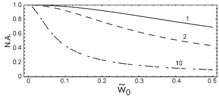
We can quantify the corresponding requirement on the ratio of trapping and addressing beam wavelengths in terms of the performance of high numerical aperture lenses. We assume a lens system with aperture diameter is used to focus the addressing light. If the ratio of the lens aperture to the Gaussian waist at the aperture is given by then a focal plane waist of implies A reasonable minimum requirement on to avoid rings surrounding the focal plane image is that the fraction of the optical power blocked by the aperture should not exceed the desired intensity ratio by more than a few times. Using an optimistic value of gives approximately 1% transmission loss at the lens and a numerical aperture of
| (1) |
The variation of the lens NA with is shown in Fig. 1. Available microscope objectives, as well as high resolution optical lithography lens systems, tend to have numerical apertures not more than unless oil immersion is used which is not compatible with atomic imaging inside vacuum chambers. This implies that the lattice light wavelength must be several times longer than the addressing wavelength in order to address single atoms with negligible leakage to neighboring sites. Thus a lattice of Rb atoms which can be manipulated with light near resonant with the D2 line at will not be individually resolvable in the context of scalable quantum logic unless
Various solutions to the addressability problem are under study. The most direct solution is to make . Arrays of widely spaced traps that use many diffractively generated beamsref.ertmer instead of lattices also fall into this category of solution. Unfortunately this is not compatible with loading from a Bose Einstein condensate via the Mott transitionref.mott , although other loading schemes may still be usedref.sw ; ref.weiss . Another possibility is to keep but load the lattice so that only every few lattice sites are occupied, or change the angle between the lattice beams after loading so that a longer periodicity is obtainedref.zoller ; ref.porto .
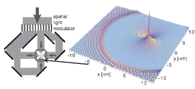
Here we analyze an alternative approach to single atom addressing in optical lattices with The idea is to accept the fact that the light cannot be localized sufficiently well, but tailor the beam profile so that the field has zeroes at neighboring lattice sites. The basic geometry is sketched in Fig. 2. beams, each with a phase controlled by a spatial light modulator pixel, propagate in the plane and are aligned to converge on the origin at The beams necessary for creating the optical lattice can in principle be combined with the imaging beams using dichroic mirrors. Each converging plane wave is polarized along with amplitude where is the azimuthal angle of wave and are adjustable amplitudes and phases. As shown in the figure this can be achieved using a single one-dimensional modulator with pixels and a system of mirrors and lenses. In the limit when and the beam amplitudes and phases are all equal the field amplitude generated on axis is just the zero order Bessel beam
When the field is synthesized from a finite number of plane waves it is quasiperiodic in space, and rings of secondary intrerference maxima occur as can be seen in Fig. 2. The diameter of the secondary rings can be estimated from Using gives , while the actual diameter found numerically is some 25% larger. Recalling the shift theorem of Fourier analysis it is straightforward to scan the spot location over a distance of up to by adding appropriate phase offsets to the incident beams, as is shown in Fig. 2. It is possible in this way to address hundreds of atoms using a multipixel modulator, without mechanical motion of the optical system. This approach to synthesis and scanning of localized optical fields also finds application in atomic lithographyref.patent .
A Bessel beam written in this way with has a central lobe with intensity radius of However the closely spaced secondary maxima of the Bessel function give crosstalk on nearby lattice sites. We describe now a method of synthesizing a beam with zeroes at regularly spaced sites of a one-dimensional lattice. An arbitrary solution of the two-dimensional Helmholtz equation can be written as a Fourier-Bessel series
| (2) |
with the complex coefficients to be determined. We have set the zero order coefficient to unity corresponding to a normalized field with unit amplitude at the origin. Any field of the form (2) can be synthesized with an amplitude and phase modulator in the geometry of Fig. 2. To make this explicit we note that the Fourier transform of (2) is
| (3) | |||||
Thus a ring of converging plane waves with wavenumber and complex amplitudes given by the term in parentheses in (3) provides the desired field. The role of the lenses shown in Fig. 2 is to tilt the wave passing through each spatial light modulator pixel towards the center of the image region, but the lenses do not tightly focus each wave. Outside of the central spot destructive interference leads to a low background light level. From the point of view of Fourier optics focusing of a beam results from interference of the constituent plane wave components, taking into account relative phase shifts due to propagation. The usefulness of the approach to image synthesis presented here is that we can directly control the amplitudes and phases of each of the plane wave components.
| max | ||||||
|---|---|---|---|---|---|---|
| 8 | 11 | 14 | 19 | |||
| 14 bit |
A field consisting of a finite number of terms in (2) that is useful for addressing a one-dimensional lattice along will have which implies that for odd. Requiring that vanish at the lattice points specified by , for and limiting the sum in (2) to terms gives linearly independent equations These equations are easily solved for the coefficients The coefficients decrease rapidly with Bessel order provided is not too much less than The series coefficients, and maximum intensity crosstalk at any site not being addressed are listed in Table 1. We see that is sufficient to ensure a crosstalk of a few times In an actual implementation there are several limiting factors to consider including the number of spatial light modulator pixels, and the amplitude and phase resolution of each one. The last row in Table 1 shows the crosstalk is up to several times higher than the theoretical value if we assume the field is synthesized from 256 beams equally spaced azimuthally, with 14 bit resolution in amplitude and phase modulation for each beam. Additional calculations with give crosstalk levels roughly 10 times lower than the example in Table 1.
In summary we have described a novel method of addressing atoms in periodic 1-D lattices with low crosstalk. The extension of this approach to a 2-D lattice is complicated by the fact that a 2-D lattice has angle dependent interatomic spacings. The Fourier-Bessel expansion (2) can still be used, but the coefficients tend to grow rapidly with Generalizations that are suitable for a 2-D geometry are currently under investigation.
This work was supported by the U. S. Army Research Office under contract DAAD19-02-1-0083, NSF, and the A. P. Sloan Foundation.
References
- (1) I. H. Deutsch, G. K. Brennen, and P. S. Jessen Fortschritte der Physik 48, 925-943 (2000).
- (2) T. Calarco, H.-J. Briegel, D. Jaksch, J.I. Cirac, P. Zoller Fortschritte der Physik 48, 945-955 (2000).
- (3) A. M. Steane, Nature 399, 124 - 126 (1999).
- (4) J. Preskill, in “Introduction to quantum computation and information,” Eds. H.-K. Lo, T. Spiller, and S. Popescu, (World Scientific , 1998).
- (5) R. Dumke, M. Volk, T. Müther, F. B. J. Buchkremer, G. Birkl, and W. Ertmer, Phys. Rev. Lett. 89, 097903 (2002).
- (6) M. Greiner, O. Mandel, T. Esslinger, T. W. Hänsch, and I. Bloch Nature 415, 39 - 44 (2002).
- (7) M. Saffman and T. G. Walker, Phys. Rev. A 66, 065403 (2002).
- (8) J. Vala, A.V. Thapliyal, S. Myrgren, U. Vazirani, D.S. Weiss, and K.B. Whaley, quant-ph/0307085.
- (9) S. Peil, J. V. Porto, B. Laburthe Tolra, J. M. Obrecht, B. E. King, M. Subbotin, S. L. Rolston, and W. D. Phillips, Phys. Rev. A 67, 051603 (2003).
- (10) P. Rabl, A. J. Daley, P. O. Fedichev, J. I. Cirac, and P. Zoller, Phys. Rev. Lett. 91, 110403 (2003).
- (11) M. Saffman, U. S. Patent application filed April 2003.