Design of photonic crystal microcavities for cavity QED
Abstract
We discuss the optimization of optical microcavity designs based on 2-d photonic crystals for the purpose of strong coupling between the cavity field and a single neutral atom trapped within a hole. We present numerical predictions for the quality factors and mode volumes of localized defect modes as a function of geometric parameters, and discuss some experimental challenges related to the coupling of a defect cavity to gas-phase atoms.
1 Introduction
A variety of passive and active optical devices can be constructed by introducing point or line defects into a periodic array of holes perforating an optically thin semiconductor slab. In such structures, light is confined within the defect regions by the combined action of distributed Bragg reflection and internal reflection. This technique has been employed in making a microcavity semiconductor (InGaAsP) laser [1] (emitting at m), and for demonstrating Si optical waveguides with sharp bends [2]. One can thus easily envision the fabrication of integrated optical “networks” on a single chip, with numerous microcavity-based active devices linked by passive waveguide interconnects.
The combination of high quality factor and extremely low mode volume that should be obtainable in point-defect microcavities makes the photonic crystal (PC) paradigm especially attractive for experiments in cavity quantum electrodynamics (cavity QED) [3], with potential applications in quantum information technology. The primary focus of this paper will be to discuss the optimization of microcavity designs for cavity QED with strong coupling between defect modes and gas-phase neutral atoms. This new paradigm for cavity QED poses formidable technical challenges with regard to atom trapping and the characterization of surface effects, so we include some discussion of these issues and of our current approaches to addressing them.
In Section II of this article we begin by analyzing elementary microcavities formed by changing either the refractive index or radius of a single defect hole. We discuss in detail some problems in previous FDTD calculations done by our group [4], as intuitions gained from the resolution of these problems are important in the microcavity design optimization for cavity QED. In Section III we present our designs of microcavities optimized for strong coupling between the cavity field and an atom trapped within a hole of the PC. Based on numerical analysis using the 3D finite-difference time-domain (FDTD) method, we predict that quality factors over can be achieved in these structures. We also discuss in this section the difficulty of estimating surface interactions between a trapped atom and the semiconductor substrate, and propose a technical strategy for confining gas-phase atoms within a defect microcavity. Finally, in Section IV we describe a procedure that we have developed for microcavity fabrication.
2 Single defect hole
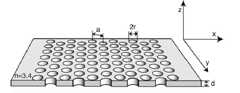
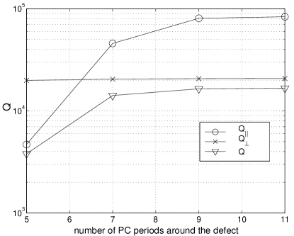
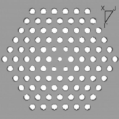
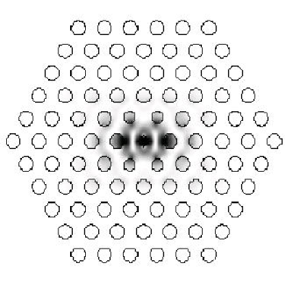
The microcavities analyzed in this paper are formed by introducing point defects into a dielectric slab patterned with a hexagonal array of air holes. The thickness of the slab is and its refractive index is equal to . The spacing between holes is denoted by and the hole radius by , as shown in Figure 1. We use to specify the optical wavelength in air. In our calculations of microcavity quality factors, the boundary for separation of vertical from lateral loss (i.e. the vertical quality factor from the lateral quality factor ) is positioned approximately at from the surface of the membrane. As the number of PC layers around a defect is increased, increases and the total quality factor approaches . We will adopt a coordinate convention in which , , denotes the center of the cavity and is the middle plane of the slab.
The simplest method of forming a microcavity within the structure shown in Figure 1 is to change the radius or index of refraction of a single hole. The former method is more interesting from the perspective of fabrication, since the lithographic tuning of geometric parameters of individual holes is a simple process, but in this section we will consider both methods. By increasing the radius of a single hole an acceptor defect state is excited, i.e., pulled into the band-gap from the dielectric band. On the other hand, by decreasing the radius of an individual hole (or by tuning its refractive index between 1 and the refractive index of the slab) a donor defect state is pulled into the band-gap from the air band [5]. Acceptors tend to concentrate their electric field energy density in regions where the larger (semiconductor) refractive index was located in the unperturbed PC, while the electric field energy density of donors is concentrated in regions where there was air in the unperturbed PC. Since the electric field intensity in air regions is small in case of acceptor defects, these are not good candidates for strong coupling with a single gas-phase atom that would be trapped within a hole. In this article we will thus focus on donor states. For a discussion of acceptor states excited in an optically thin slab perforated with a hexagonal PC array, readers are referred to Ref. [6].
2.1 Changing the refractive index of a single hole
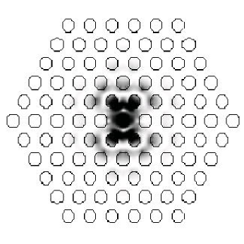
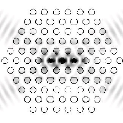
Microcavity formation by alteration of the refractive index of a single defect hole in a hexagonal PC has been analyzed previously by our group [4]. In that analysis, we predicted that dipole-like donor states (such as the -dipole mode shown in Figure 2) with quality factors up to should exist. We now believe that the quality factors of such microcavities are limited to several thousand, for reasons discussed below. This discussion reveals the extreme sensitivity of microcavity quality factors to small distortions to the local PC geometry, which will later be used as a powerful design tool in optimization for cavity QED.
In our previous work, mirror boundary conditions were applied in the , and directions to achieve an eight-fold reduction in the computational grid size. We have since realized that the manner in which even (symmetric) mirror boundary conditions are implemented in our finite-difference time domain (FDTD) code results in numerical output that properly corresponds to an analyzed structure with slight deformations relative to the intended structure. For example, the set of mirror boundary conditions used to select the -dipole mode in a defect cavity leads to a deformation of the structure as shown in Figure 3. Holes on the -axis (including the defect) are elongated in the direction by 1 point but the distance between holes in and directions is preserved. Because hole-to-hole distances are preserved under this deformation, the half-spaces and actually maintain the unperturbed PC geometry when holes in the central row are elongated by points in both the directions. The symmetry of the PC surrounding the defect is therefore broken, and this contributes to artificially high quality factors for -dipole modes. An even mirror BC was also applied in the direction in our previous analysis, causing a slight error in the thickness of the slab. The correct ratios of the structures analyzed in Ref. [4] would be 0.6, 0.46 and 1, instead the values of 0.53, 0.4 and 0.93, as noted there.
2.1.1 Perfectly symmetric cavity
We re-analyzed the structure with , , , the refractive index of the slab equal to , 5 layers of holes around the defect, and grid points. For this set of parameters, the predicted in Ref. [4] for the -dipole mode was . In the present analysis, even mirror boundary conditions were applied to the lower boundary in the direction only, to reduce the computation size by one half and to eliminate TM-like modes. Absorbing boundary conditions were applied to all boundaries in and directions and to the upper boundary in direction. Under these BC’s the intended symmetry of the defect structure was achieved. The initial field distribution was chosen in such a way as to excite or dipole modes selectively. For the -dipole mode we now calculate , and , and for the -dipole mode we calculate , and .
The difference between parameters computed for the and dipole modes comes partly from the asymmetry of the structure introduced by imperfect discretization. In a 2D PC with infinite slab thickness, these two modes should be degenerate [4]. In the thin slab however, the -dipole mode suffers more vertical scattering at the edges of holes and, therefore, has a lower . For a non-symmetric applied initial field distribution leading to excitation of both and dipole modes, we calculated , and . This mode can be represented as a superposition of the and dipole, with weighting factors depending on the initial field. Its quality factor and resonant frequency depend on these weighting factors.
2.1.2 Asymmetric cavity
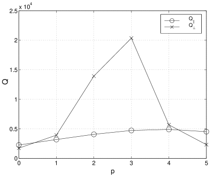
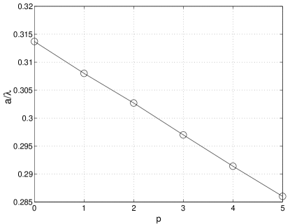
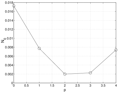
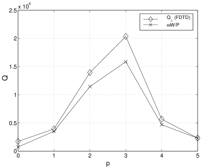
Our explanation for the discrepancy between our current and previous results leads us to ask whether a “real” (intentional) elongation of the central row of holes along the -axis may actually improve the quality factor () of the -dipole mode. A possible disadvantage of this approach is the excitation of additional states caused by enlarging holes in the central row. We have therefore analyzed how and of the -dipole mode in this structure changes as a function of the elongation parameter . Holes on the -axis (including the defect) are elongated in both the directions by points, in such a way that hole-to-hole distances are preserved and the half-spaces and maintain the unperturbed PC geometry. The structure parameters are , , , and 5 layers of holes surround the defect. The periodicity used in these calculations is equal to grid points, and the elongation step corresponds to . The results are shown in Figure 4. It is interesting that the frequency of the mode decreases as increases, even though the amount of low refractive index material increases. However, the net amount of low refractive index material does not matter; what does matter is where the low refractive index is positioned relative to the unperturbed PC. The explanation of the decrease in frequency is very simple, if we recall the -dipole mode pattern shown in Figure 2. This is a donor type defect mode, which concentrates its electric field energy density in low refractive index regions of the unperturbed PC. As increases, layers of PC holes are moved away from the defect in direction. For example, the -th layer of holes parallel to the -axis will be positioned at , instead of . Therefore, a large refractive index material will be positioned at places where the mode expects to “see” air, leading to a decrease in mode’s frequency. By tuning the mode’s frequency across the band-gap, we can also tune its factor, as noted previously [6]. For , reaches the value of . The analyzed -dipole mode mostly resonates in the direction of -axis, i.e. in the direction of photonic crystal. The tuning of the elongation parameter is, therefore, analogous to tuning of a spacer in the micropost cavity, which leads to tuning of mode’s frequency and factor. A more detailed explanation of the effect of elongations on factors is given in the appendix of this article. By increasing the number of PC periods around the defect, the total quality factor approaches , as shown in Figure 5. It is important to note that does not increase exponentially with the number of PC layers around the defect. Instead, it saturates at large number of PC layers. The reason is in the choice of a boundary for separation of from , positioned at approximately from the surface of the membrane.
From the radiation pattern of the -dipole mode, we can see
that some portion of the out-of-plane loss (mostly in the
direction) still gets collected in . This loss cannot be
suppressed by increasing the number of PC layers around the
defect, and it determines the value at which saturates.
However, much larger out-of-plane loss is collected in , which ultimately determines the total quality factor .
Therefore, a dramatic improvement in factors of dipole modes over single defect microcavities can be obtained by introducing a novel type of PC lattice defect, consisting of the elongation of holes along the symmetry axes. We call it a fractional edge dislocation, by analogy with edge dislocations in solid state physics. Edge dislocations are formed by introducing extra atomic planes into the crystal lattice. On the other hand, we here insert only fractions of atomic planes along the symmetry axes of photonic crystal.
Unfortunately, at this time, we do not know how to control
the refractive index of a single PC hole during the fabrication.
For this reason, in the next subsection we will consider
alternative methods of forming single defect microcavities, which
are much easier to construct by microfabrication.
Even after the elongation of holes on the -axis by 1 point, factors of were not obtained. This means that the application of mirror BC at and planes causes additional effects that lead to the overestimation of quality factors. One of the reasons may be that the excited dipole mode does not have a symmetry described by the applied discretized mirror BC’s. This may be partly due to the structure imperfection caused by discretization. In order to avoid problems caused by BC’s all the calculations in this paper were done by applying the even mirror symmetry to plane only, in order to select TE-like modes and to reduce the computation size by one half. Absorbing boundary conditions were applied to all boundaries in and directions and to the upper boundary in the direction. To prove that the application of mirror BC at the lower boundary does not change , we also analyzed entire structures with absorbing BC’s applied to all boundaries and obtained the same results as in the analysis of one half of the structure.
| 0.275 | 0.15 | 0.75 | 0.286 | 778 | 920 |
| 0.275 | 0.2 | 0.75 | 0.297 | 470 | 2078 |
| 0.25 | 0.15 | 0.75 | 0.277 | 230 | 1840 |
| 0.25 | 0.2 | 0.75 | 0.284 | 116 | 3190 |
2.2 Reducing the radius of a single hole
Microcavities analyzed in this subsection are formed by reducing the radius of a single hole to . We calculated parameters of excited dipole modes for a range of microcavity parameters and results are shown in Table 1. For all tabulated results, 5 layers of holes surround the defect and . Calculated ’s are not very impressive, but they do provide us with a good starting point for further optimization. Why did we decide to use a relatively small ratio for the PC? According to our calculations, increasing within the analyzed range leads to increases in the band gap and reduction of lateral losses. However, vertical scattering at the edges of holes also increases and drops. It is therefore important to find an optimum which leads to small vertical losses but preserves good lateral confinement, in order not to increase the mode volume too much.
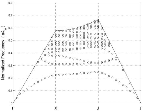
The band diagram for TE-like modes of a thin slab (, ) surrounded by air on both sides and patterned with a hexagonal array of air holes () is shown in Figure 6. These PC parameters are used in most of the calculations in the next section. From the comparison of the dipole mode frequencies tabulated in Table 1 and the band diagram shown in Figure 6, it can be confirmed that as the cavity mode’s frequency approaches the bottom of the air band, vertical losses decrease, but lateral losses increase, which in turn leads to an increase in the mode volume. Our goal in the next section will be to reduce vertical losses and improve factors even further, while preserving small mode volumes. For this purpose we will explore fractional edge dislocations. In Figure 4, one can observe that an increase in the elongation parameter can be used to tune the factor of a mode, but also leads to a decrease in the dipole mode’s frequency. This implies that by increasing , the mode is pulled deeper into the band gap, away from the air band edge, which leads to its better lateral confinement . Therefore, we can simultaneously achieve a reduction in vertical losses and an improvement in lateral confinement (i.e. an increase in both and , and a reduction in the mode volume).
3 Cavities for strong coupling
In this section we consider the design of PC microcavities to achieve strong coupling between the cavity field and a single gas-phase atom, that is, an atom located in free space rather than contained as an impurity in the dielectric slab. Our long-term goal is to investigate photonic bandgap structures for single-atom cavity quantum electrodynamics in the strong coupling regime [3]. For this purpose, the microcavity mode quality factor () has to be as large as possible and the mode volume () as small as possible. These two design rules are also followed when designing PC microcavities for semiconductor lasers. However, in a cavity for strong coupling, an atom must be trapped at the point where it interacts most strongly with the cavity field. Therefore, an additional design goal is imposed in this case: the cavity mode should have the E-field intensity as high as possible in the air region. When designing a laser cavity, the problem is opposite: one tends to maximize the overlap between the gain region and the cavity field and, therefore, wants to have the strongest E-field in the semiconductor region.
Mode volume (), critical atom () and photon () numbers are defined as follows:
| (1) | |||||
| (2) | |||||
| (3) |
where is the cavity field decay rate, proportional to the ratio of the angular frequency of the mode () and the mode quality factor ():
| (4) |
is the atomic dipole decay rate ( MHz for Cesium) and is the coupling parameter at the point where we want to put an atom:
| (5) |
denotes the vacuum Rabi frequency:
| (6) | |||||
| (7) |
Strong coupling is possible if both and are smaller
than 1. Therefore, in order to predict whether the strong coupling
can occur, we must calculate upper limits of and and
compare them to 1. In other words, it is acceptable if calculated
critical numbers are overestimated. As the number of PC layers
around the defect increases, the total quality factor
approaches and drops due to the better
lateral confinement. Hence, we can calculate and by
assuming
and using calculated for 5 PC layers around the defect.
For all calculations in this section, the refractive index of the
slab is , 5 layers of holes surround the central hole and
. The elongation step corresponds to ,
i.e. of the lattice periodicity . The material and PC
properties are chosen in such a way that cavities operate at
nm (the wavelength corresponding to the D2 atomic
transition in ).
3.1 Single defect with fractional edge dislocations
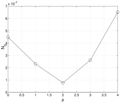
Let us study microcavities formed by reducing the radius of a single hole and simultaneously applying a fractional edge dislocation (of order ) along the -axis. It is important to note that all holes along the -axis are elongated in this process, including the defect hole of the reduced radius. We will calculate the dependence of the -dipole mode properties on parameter . Parameters of the unperturbed PC are: , , and the defect hole radius is . The critical atom () and photon () numbers are shown as a function of the elongation parameter for the -dipole mode in Figure 7. does not change significantly with and it is approximately equal to for all structures. When increases, the frequency of the mode moves away from the band edge, towards the center of the band gap, increases and peaks at the value of for .
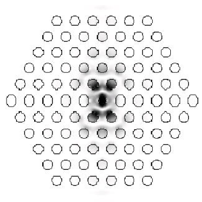
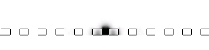
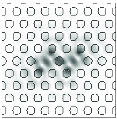
From the electric field intensity pattern of the -dipole mode shown in Figure 8, one can see that the electric field intensity is very strong within the defect hole. Therefore, an atom trapped there should interact very strongly with the cavity field. From the calculated critical atom and photon numbers, it then should be possible to achieve very strong coupling. At , the parameters of such a cavity are , , and . Due to extremely small mode volumes in these cavities, strong coupling is possible even for moderate values of , as did not exceed in the parameter range of Fig. 7. Furthermore, is much smaller than , which means that we can try to improve factors further at the expense of increasing . factors above and similar values of and can also be obtained for the cavity consisting of a single defect with and a fractional edge dislocation of order , produced in the photonic crystal whose parameters are , and .
3.2 Tuning holes around the defect
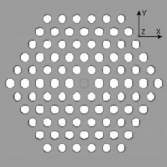
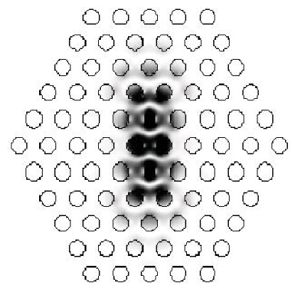
Dipole modes are particularly sensitive to the geometry of holes closest to the defect. By tuning these holes, we can induce frequency splitting of dipole modes and dramatically influence their factors. In Ref. [4], the variation of two nearest neighbor holes along the -axis was analyzed. Here, we will test the influence of changing 4 holes closest to the defect in directions. The analyzed structure is shown in Figure 9. The radius of the central hole is reduced to and the radii of the 4 closest holes in directions are reduced to . These 4 holes are simultaneously moved away from defect, by in directions, which preserves the distance between them and the next nearest neighbors in the same directions. This design will improve the factor of the -dipole mode and spoil the of the -dipole mode. We analyzed structures with various parameters, but our best result was obtained for , , , and . The electric field intensity pattern of the excited -dipole mode is shown in Figure 10, and its calculated parameters are and . From Table 1 we can see that a dipole mode excited in a single defect microcavity with this , , has . Therefore, the tuning of 4 holes can lead to a substantial increase in of the -dipole mode. The disadvantages of this design include the excitation of defect modes other than dipoles (coming from variation of several holes).
Let us try to improve of this cavity even further, by also employing the idea of elongation of holes along desired directions. Our mode of choice is the -dipole and we will elongate holes sitting on the -axis by points in the direction in such a way that the half-spaces and remain the unperturbed PC geometry. The dependence of (which decreases with ) on parameter is shown in Fig. 11. does not change significantly with and is in the range between and . The calculated is around for all structures. Again, a very strong coupling is achievable by this design, and we note that at the point achieves a value .
3.3 Atomic physics
Given that microcavities with strong coupling parameters can be designed and fabricated, two further technical issues must be addressed in order to establish the feasibility of cavity QED with neutral atoms in PC’s. First, we must identify a method for stably trapping an individual atom within a hole of the PC. Second, accurate estimates or measurements must be made of the surface interaction between such a trapped atom and the semiconductor substrate. Although definitive solutions to these challenges are the subject of future work, we include in this subsection a brief discussion of each topic.
In addition to the creation of photonic crystals, modern micro-fabrication techniques enable the patterning of either conductive wires or ferromagnetic materials at the micron scale and below. As a result, it should be possible to construct magnetic microtraps with field curvatures G/cm2 [7, 8, 9, 10]. With this magnitude of field curvature an Ioffe trap could hold a Cs atom with Lamb-Dicke parameter in the radial direction, yielding nm in the ground state of the trapping potential and enabling resolved-sideband laser cooling as a means of putting single atoms in the ground state.
We are currently investigating fabrication and laser cooling techniques for an atom-trapping scheme in which micron-scale wires would be deposited on the surface of the PC semiconductor substrate, such that the circular wire pattern of an Ioffe microtrap are arranged concentrically around a defect microcavity. The trap designs discussed in [7] have sufficiently large inner diameter not to disturb the photonic bandgap structure of the defect cavity. Such a wire arrangement would project a magnetic field with a stable minimum at the geometric center of the microcavity, such that one or more atoms could be confined within the defect hole and would therefore experience strong coupling. A similar geometry could be envisioned for microtraps based on permanent magnets rather than current-carrying wires, which would have significant advantages in terms of heat load to the PC substrate.
A neutral atom trapped within a hole of a PC structure will experience surface (van der Waals) interactions that are quite difficult to estimate. The significance of such interactions is twofold. The sensitive dependence of the ground state energy shift on an atom’s position will lead to mechanical forces that must be compensated by the trap design. Differential shifting of the atomic ground and excited states on the cavity QED transition must also be accounted for, as this will introduce a position-dependent detuning relative to the fixed microcavity resonance. Although van der Waals shifts can be computed for alkali atoms near dielectric or metallic boundaries with simple symmetry [11, 12], the case of an atom in a PC hole is far more complex. The local geometry seen by a trapped atom will be that of a cylindrical hole with finite extent, and a proper calculation must take into account the overall modification of vacuum modes due to the extended photonic crystal.
Furthermore, the resonant frequencies of many atomic transitions that connect to low-lying states, and therefore contribute strongly to their van der Waals shifts, are above the bandgap of the semiconductor substrate. Such transitions will “see” an absorptive surface while those below the bandgap will see a dielectric surface. This set of factors brings the complexity of the desired calculation well beyond that of existing analytic results in the literature. It should be noted that experimental measurements of the van der Waals shifts in our proposed system would be of significant interest for the general subject of quantum electrodynamics of semiconductors.
We are pursuing a numerical strategy for estimating the magnitude of surface interactions. In a linear response approximation, it should be possible to compute leading-order contributions to the van der Waals shifts from FDTD simulations of the electromagnetic field created by an oscillating dipole source in the photonic crystal structure. While the nature of the code does not allow us to compute directly the backaction of the scattered field on the source dipole, we believe that elementary field theory can be used to relate the simulated field to van der Waals shifts. Our findings will be reported in a forthcoming publication.
3.4 Coupled dipole defect modes
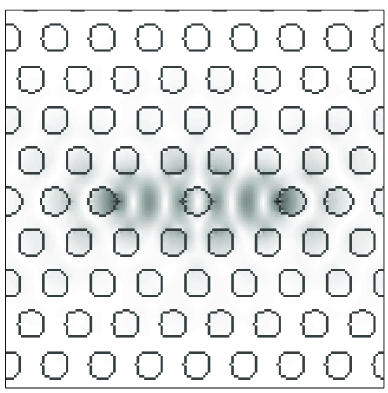
The significance of surface effects that could perturb atomic radiative structure within the small defect hole is still unknown. For that reason, we will try to investigate ways of increasing the radius of the hole where the coupling between the atom and the cavity field should occur. Let us now analyze the cavity design where the strong E-field intensity can be achieved in the center of an unperturbed hole. The idea is to use coupling of two dipole defect states. Resonant modes of the microcavity formed by coupling two single defects are presented in Figure 12. Based on the resultant electric field intensity in the central, unperturbed hole, we call them constructively or destructively coupled defect states. They have different frequencies, as well as factors. We will analyze properties of the constructively coupled state, since the central, unperturbed hole would be a good place for an atom.
We analyzed a series of structures with different parameters. The best results were obtained for two coupled defects with in a PC with the following parameters: , , and . Holes in the direction, in columns containing defects, are elongated by 2 points in the direction. The mode pattern of the constructively coupled defect state is shown in Figure 13. Parameters of the mode are: , , , and . An atom can now be trapped in the central hole of unperturbed radius. For , this radius is , which is a significant improvement over the previous design, where an atom must be trapped within a radius hole. Again, a strong coupling is achievable in this cavity.
An alternative way of forming the coupled defects state is represented in Figure 14. We use the same PC parameters as previously: , , , and . Holes in rows containing defects, are elongated by 2 points in the direction.
The mode pattern of the constructively coupled defect state is shown in Figure 14. Parameters of the mode are: , , , and . Strong coupling is achievable for an atom trapped in any of the two central holes of the unperturbed radius (positioned between the defects). For , this radius is again .
4 Fabrication
We have recently developed the fabrication procedure for making these cavities in . The material and PC properties are chosen in such a way that cavities operate at (the wavelength corresponding to the atomic D2 transition in ).
The fabrication process starts by spinning of thick high molecular weight PMMA (polymethylmethacrylate) on top of the wafer. The PMMA layer is subsequently baked on a hot plate at for 20 minutes. A desired 2D PC pattern is beamwritten on the PMMA by electron beam lithography in a Hitachi S-4500 electron microscope. The exposed PMMA is developed in a 3:7 solution of 2-ethoxyethanol:methanol for 30 seconds. The pattern is then transferred into the layer using the assisted ion beam etching. After that, the sacrificial layer is dissolved in hydrofluoric acid (HF) diluted in water. HF attacks very selectively over for [13]. Therefore, the percentage of in our layer is around . Finally, the remaining PMMA may be dissolved in acetone.
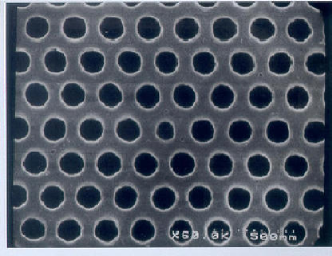
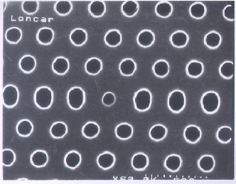
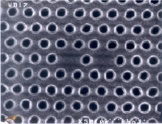
Three SEM pictures showing top views of fabricated microcavity structures are shown in Figure 15. We are currently working to measure the passive optical properties of such microcavities in order to validate our theoretical predictions.
5 Conclusion
In conclusion, we have theoretically demonstrated that PC cavities can be designed for strong interaction with atoms trapped in one of PC holes. At present, we are working on further optimization of the design and the characterization of fabricated structures.
Critical issues for further investigation include efficient coupling of light in and out of the PC microcavity, as well as accurate estimation of surface effects that could perturb atomic radiative structure within the small defect hole. The extremely small mode volume in these structures also poses an interesting theoretical question of how standard cavity QED models must be modified when the single-photon Rabi frequency exceeds the atomic hyperfine spacing.
6 Appendix: The effect of fractional edge dislocations
Any wavefront can be considered as a source of secondary waves that add to produce distant wavefronts, according to Huygens principle. Let us assume that we know the field distribution accross the plane , positioned in the near field, above the free standing membrane and in parallel to the membrane surface. The far fields can be considered as arising from the equivalent current sheets on this plane. Therefore, we can calculate the far field distribution and the total averaged radiated power into the half-space above the plane [14]:
| (8) |
where and represent radiation vectors, whose components in the rectangular coordinate system are proportional to Fourier transforms of tangential field components at the plane [15]:
| (9) | ||||
| (10) | ||||
| (11) | ||||
| (12) | ||||
| (13) | ||||
| (14) |
Therefore, just by knowing the Fourier transforms of the tangential field components at the plane , we can evaluate the time averaged radiated power . From the previous expressions it is clear that the wave-vector of interest lies within the light cone for any values of angles and in the circular polar coordinate system (i.e. ). This implies that the radiated power depends only on the wave-vector components located within the light cone. It is also clear that by suppressing the Fourier components within the light cone, one can reduce . Having in mind that for the -dipole mode and fields are odd with respect to both and symmetry axes, and do not contribute significantly to the integral in expression 8 (they are both equal to zero at any point in the k-space with either or equal to zero). On the other hand, and field components are even with respect to both and axes and their Fourier transforms are generally non-zero at small wave-vector values. However, by tuning the elongation factor , one can balance the energy in the positive and negative field lobes and minimize the Fourier components of and within the light cone. This also leads to a decrease in the radiated power . We can conclude that the improvement in the factor after the application of fractional edge dislocations is due to the suppression of the wave-vector components composing the defect mode, which are located within the light cone. A more detailed explanation of this phenomenon and how it can be used to improve factors of other types of modes will be presented in our forthcoming publication[15].
The factor of a mode can be expressed as
, where is the total energy of a mode in
the half-space . The comparison between the factor
calculated using the method presented in this appendix, and
previously estimated using the FDTD, for the structure
from the subsection 2.1.2, is shown in Figure
16. The plane is positioned directly above the
surface of the membrane in this case. From Figure
5 it follows that the total factor saturates
at about , when the number of PC layers around the defect
increases in the structure with . This is very close to the
maximum value estimated from the expression 8.
Acknowledgement
This work has been supported by the Caltech MURI Center for Quantum Networks.
References
- [1] O. Painter, R.K. Lee, A. Scherer, A. Yariv, J.D. O’Brien, P.D. Dapkus, and I. Kim. Two-Dimensional Photonic Band-Gap Defect Mode Laser. Science, 284:1819–1821, June 1999.
- [2] M. Lončar, D. Nedeljković, T. Doll, J. Vučković, A. Scherer, and T. P. Pearsall. Waveguiding at 1500nm using photonic crystal structures in silicon on insulator wafers. Applied Physics Letters, 77:1937–1939, September 2000.
- [3] H. J. Kimble. in Cavity Quantum Electrodynamics, edited by P. Berman. Academic Press, San Diego, 1994.
- [4] O. Painter, J. Vučković, and A. Scherer. Defect Modes of a Two-Dimensional Photonic Crystal in an Optically Thin Dielectric Slab. Journal of the Optical Society of America B, 16(2):275–285, February 1999.
- [5] E. Yablonovitch, T.J. Gmitter, R.D. Meade, A.M. Rappe, K.D. Brommer, and J.D. Joannopoulos. Donor and acceptor modes in photonic band-structure. Physical Review Letters, 67:3380–3383, 1991.
- [6] J. Vučković, M. Lončar, and A. Scherer. Design of photonic crystal optical microcavities. Proceedings of SPIE, Photonix West 2001, 2001.
- [7] J. D. Weinstein and K. G. Libbrecht. . Physical Review A, 52:4004, 1995.
- [8] M. Drndić, C. S. Lee, and R. M. Westervelt. Three-dimensional microelectromagnet traps for neutral and charged particles. Physical Review B, 63:085321, 2001.
- [9] J. Reichel, W. Hansel, P. Hommelhoff, and T. W. Hansch. Applications of integrated magnetic microtraps. Applied Physics B, 72:81, 2001.
- [10] M. Bartenstein, D. Cassettari, T. Calarco, A. Chenet, R. Folman, K. Brugger, A. Haase, E. Hartungen, B. Hessmo, A. Kasper, P. Kruger, T. Maier, F. Payr, S. Schneider, and J. Schmiedmayer. Atoms and wires: Toward atom chips. IEEE Journal of Quantum Electronics, 36:1364, 2000.
- [11] G. Barton. Van der Waals shifts in an atom near absorptive dielectric mirrors. Proceedings of the Royal Society of London A, 453:2461–2495, 1997.
- [12] Martine Chevroliier, Michele Fichet, Marcos Oria, Gabriel Rahmat, Daniel Bloch, and Martial Ducloy. High resolution selective reflection spectroscopy as a probe of long-range surface interaction: measurement of the surface van der Waals attraction exerted on excited Cs atoms. Journal de Physique II, 2:631–657, 1992.
- [13] E. Yablonovitch, D.M. Hwang, T.J. Gmitter, L.T. Florez, and J.P Harbison. Van der Waals Bonding of GaAs Epitaxial Liftoff Films onto Arbitrary Substrates. Applied Physics Letters, 56(24):2419–2421, June 1990.
- [14] S. Ramo, J.R. Whinnery, and T. Van Duzer. Fields and waves in communication electronics. John Wiley and Sons, Inc., New York, 1994.
- [15] J. Vučković, M. Lončar, H. Mabuchi, and A. Scherer. Optimization of Q-factor in microcavities based on free-standing membranes. IEEE Journal of Quantum Electronics, 38(7):850–856, July 2002.