Photoconductance Quantization in a Single-Photon Detector
Abstract
We have made a single-photon detector that relies on photoconductive gain in a narrow electron channel in an AlGaAs/GaAs 2-dimensional electron gas. Given that the electron channel is 1-dimensional, the photo-induced conductance has plateaus at multiples of the quantum conductance 2e2/h. Super-imposed on these broad conductance plateaus are many sharp, small, conductance steps associated with single-photon absorption events that produce individual photo-carriers. This type of photoconductive detector could measure a single photon, while safely storing and protecting the spin degree of freedom of its photo-carrier. This function is valuable for a quantum repeater that would allow very long distance teleportation of quantum information.
pacs:
72.20.-i, 72.40.+w, 73.23.-b, 73.63.-b, 78.67.-nThe detection of individual photons has become common in the last few decades with the proliferation of avalanche photodetectors, Yoshizawa01 and negative electron affinity Antypas74 photocathode photomultipliers. However, it is becoming desirable now to transmit something more sophisticated than single-photon states. Namely, we want to distribute quantum entanglement information over long distances to enable teleportation Bennett93 and other forms of advanced telecommunication. For this, single-photon sensitivity is not enough. New types of single-photon photodetectors are needed, which preserve the spin information of the photo-carrier.
New selection rules have been identified in the III-V semiconductor photodetectors, that permit the transfer Vrijen01 of photon polarization information directly to photo-electron spin. Unfortunately, the avalanche multiplication process is relatively violent, of necessity, and it destroys any spin information that might have been present on the original photo-electron. New forms of single-photon detection have been developed recently, that are gentle enough to preserve the photo-electron spin state, while providing the gain needed to detect a single photon. For example photoconductive gain can provide for single-photon detection.
Shields et al.Shields00 recently demonstrated single-photon sensitivity in a two-dimensional (2D) electron channel controlled by photoelectric charge trapped on adjacent InxGa1-xAs precipitates in AlGaAs. In photoconductive gain, electric charges become trapped for long periods, and while trapped, their electric charge can influence the channel conductivity. Over time, vast amounts of electric charge can be transferred in the channel current, far more than the original trapped charge, creating a huge photoconductive gain. Trapping of an individual photo-carrier produces a step function in current that can persist for long periods. In AlGaAs alloys at low temperature this is called persistent photoconductivity, and the current can last for weeks. An analogous electrical transport sensitivity enhancement was spectacularly used to detect individual far-infrared photons by Komiyama et al.Komiyama00
In this report, we demonstrate that an ordinary, conventional, AlyGa1-yAs/GaAs modulation-doped field effect transistor, in a 2D electron gas quantum point contact configuration, can already detect single-photon events. InxGa1-xAs precipitates in GaAs are unnecessary, as the ordinary defect centers that are already present in AlyGa1-yAs/GaAs can trap photo-carriers successfully. Furthermore, the trapped photocharge has the same effect as a positive external gate in un-pinching the channel, leading to conductance quantization steps. Thus we are in the interesting situation where individual single-photon-conductivity steps are superimposed on the 1D channel conductance quantization steps associated with a variable width point contact channel. As an aside, this may also be the first observation of photo-induced 1D channel conductance quantization.
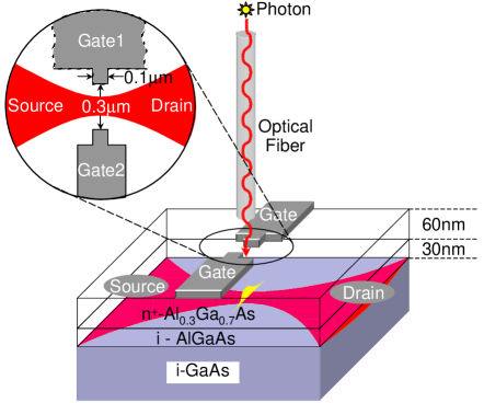
The sample used for these experiments is a modulation-doped heterostructure with a quantum point contact defined by a pair of split gates on Al0.3Ga0.7As/GaAs, as illustrated in Fig. 1. All layers are grown by molecular beam epitaxy on semi-insulating GaAs, consisting of a nominally undoped GaAs buffer layer, an i-Al0.3Ga0.7As spacer layer 30 nm thick, a Si-doped (11018cm-3) n-Al0.3Ga0.7As layer 60 nm thick, and a Si-doped GaAs cap layer, 5 nm. The 2D electron gas in the heterointerface has a carrier density of 3.31011 cm-2, a mobility of 1.1106 cm2/V s and a Fermi energy (EF) of 1.8 meV. The Ti/Au split gate, of lithographic length 0.1 m, and spacing 0.3 m, is fabricated on the heterostructure using electron-beam lithography and electron-gun evaporation. The 1D channel is formed as a line by depletion in the 2DEG between the two gates.
The sample is illuminated by monochromatic light through a large-core glass fiber, that is carefully shielded to block any photons from the outer jacket. The light is created by a tungsten lamp and then filtered by a monochromator, a long-pass filter passing wavelengths 530 nm, and a 20 dB neutral density filter. The optical power at the end of the fiber measured by a Si detector is 9 pico-Watts. The area of illumination at the device is about 1 mm in diameter due to end-fire coupling from the fiber. Given the small device area 310-10 cm2 defined by the gates, we estimate the actual light power in the active area to be 710-9 times smaller. Thus the incident photon flux is estimated to be 0.1 photon per second on the effective device area.
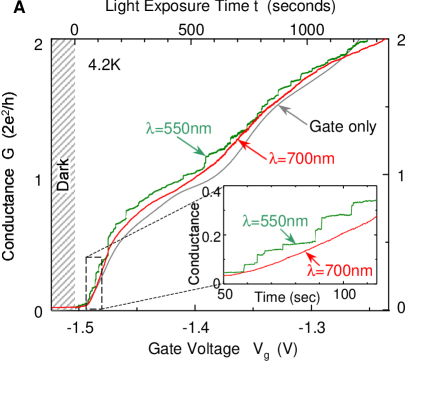
The source/drain current is measured at a constant voltage drop (VSD) of 0.5 mV, at a temperature of 4.2 K. Figure 2A shows the corresponding source/drain conductance, as a function of either gate voltage, or of the light exposure time. As the channel is opened up, a series of electron wave-guided modes successively contribute conductance steps,van Wees88 ; Wharam88 in units of the conductance quantum, 2e2/h 1/13,000 , where e is the electronic charge, the factor 2 accounts for spin, h is Planck’s constant, and is Ohms. The first two steps are shown in Fig. 2A, and their sharpness is consistent with the temperature, 4.2 K. In addition there is a well-known Thomas96 shoulder at conductance 0.7 (2e2/h) thought to be associated with electron spin exchange interaction Wang98 effects.
What is remarkable about Fig. 2A is that there are two different physical phenomena, producing almost identical source/drain conductance on the vertical axis. The curve labeled “gate only” shows that positive gate voltage, above the -1.5 Volt gate threshold, opens up the electron channels producing conductance steps. Likewise, exposure to a weak light source of wavelength = 700 nm, at a fixed bias voltage produces trapped positive charge that also opens up the electron waveguide channels, producing exactly the same conductance steps. In fact the processes are the same. In either case, positive net charge opens up the source/drain electron current channels, leading to the observed electron conductance steps.
An enduring, photo-induced, increase in conductivity has been well known Nelson77 ; Kastalsky84 ; Wei84 in III-V semiconductors, and is called persistent photoconductivity. At temperatures much lower than 100K the net positive trapped charge, is known to persist for weeks. The photo-exposure begins at time t = 0 in Fig. 2A, to the right of the crosshatched dark region where the conductivity begins as a constant. If the photo-exposure is prematurely terminated, the conductance becomes constant again in Fig. 2A, persisting at the new value for weeks.
Photoconductivity in an electron channel requires fixed positive charge from trapped photo-holes. The hole trapping centers can be either neutral donors d0, that become ionized undergoing the transition d0 + h+ d+, or they can be DX- centers Lang77 ; Lang79 ; Chadi88 ; Chadi89 ; Linke98 that become neutralized by hole capture,Brunthaler89 DX- + h+ d0. In any case, the net trapped positive charge has the same effect on the source/drain electron channel as positive gate increments do. The only difference in Fig. 2A is that the horizontal axis at the top measures the net positive charge in terms of optical exposure time from a weak = 700 nm beam, and the horizontal axis at the bottom measures positive increase of gate voltage. The same quantum conductance plateaus are produced in either case.
When the photon wavelength is reduced to = 550 nm, well beyond the Al0.3Ga0.7As bandgap, an additional phenomenon appears, that is plotted in Fig. 2A, as the curve labeled “ = 550 nm”. That curve still follows the overall shape of the quantized conductance steps, but the curve itself consists of many smaller steps that, in aggregate, produce the quantized conductance shape, including the 0.7 (2e2/h) feature. The smaller steps, we attribute to absorption of individual photons, and the corresponding capture of a single photo-hole. Since the traps are at variable distances from the source/drain channel, each photon produces a different step height. This is different from the Millikan oil-drop experiment, but similar to the observations by Shields et al.,Shields00 who trapped photo-holes on InGaAs islands.
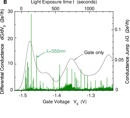
The photon steps for = 550 nm in Figs. 2A seem to be taller where the conductance curve is steeper, due to greater sensitivity to electrostatic charge changes when dG/dVg is larger. This point is illustrated in Fig. 2B, that plots: (1) dG/dVg versus gate voltage on the left and bottom axes, and on the same graph, (2) G, single-photon step height versus photon exposure time on the right and top axes, respectively.
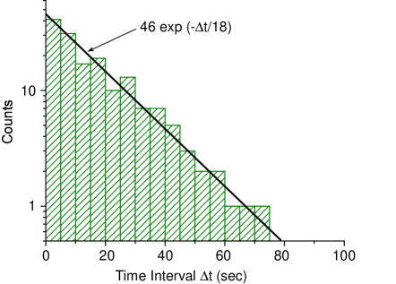
The = 550 nm “curve” in Fig. 2A is seen in Fig. 2B to consist of about 70 individual photon steps. We can test for proper photon statistics by plotting a histogram of the time intervals between photon events, as illustrated in Fig. 3. The intervals should fall on a decaying exponential for random photon events, as is appropriate for un-squeezed photon statistics, with the average interval between photon events being 18 seconds in this case. This low photon detection rate is consistent with an active area of 310-10 cm2, and a quantum efficiency of around 30%. The monotonic upward conductance changes are to be distinguished from “random telegraph signal”, Ralls84 that fluctuates in either direction.
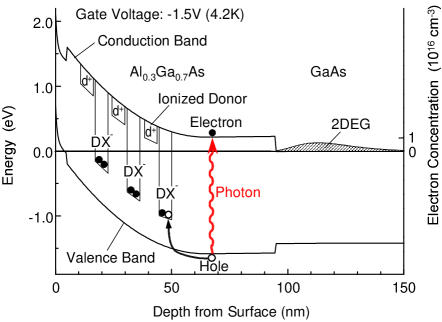
The wavelength dependence of the onset of the single-photon-conductivity steps is correlated with the 1.9 eV bandgap of the Al0.3Ga0.7As layer, on top of the 2D electron gas. The onset of single-photon steps begins at wavelengths shorter than 650 nm, becoming more pronounced at = 550 nm where the Al0.3Ga0.7As is more absorbing. By contrast, the single-photon steps are not seen at = 700 nm. A corresponding model of the photo-conductive process at = 550 nm is illustrated in Fig. 4. A photon is absorbed in the Al0.3Ga0.7As layer, with the photo-hole being trapped at DX- centers that are associated with the n-type doping. Alternately the photo-hole can be trapped at neutral donors, d0, though none are shown in Fig. 4. (According to the negative-U property DX of DX- centers, neutral donors segregate into ionized donors d+ and DX- centers.) Regardless, in either case, the net increase in positive charge among the donor defects opens up the source/drain channel creating a permanent increase in electron current.
In converse, at = 700 nm, photons are absorbed in the nominally undoped GaAs buffer layer, which is usually weakly n-type. Thus the photo-hole recombination centers, residual neutral donors d0, are very dilute. They are too far away from the source/drain channel to produce noticeable discrete jumps in current for single-photon events at = 700 nm. Nonetheless, the smooth photoconductance channel quantization steps are still observed at = 700 nm, as shown in Fig. 2A.
The photo-electron plays a lesser role. It usually ends up in the channel, and then becomes swept away in the source and drain electrodes. Since those are ohmic contacts, they can continue to inject replacement electrons indefinitely. This is essentially the mechanism Rose78 of secondary photoconductivity and photoconductive gain that is responsible for the single-photon sensitivity.
The conductance curve in Fig. 2A ends at the 2 conductance units (2e2/h) plateau. Above this conductance level, the gate-induced and photo-induced conductance changes no longer match. The photo-induced conductance change tends to saturate above 2 conductance units (2e2/h), after about 70 discrete photon conductance steps, but the gate-induced change continues to higher conductance. We attribute the saturation of the photo-induced conductance to saturation of the doping-induced trapping centers. Within the active area of 310-10 cm2 there are 3.31011 carriers/cm2 or only about 100 carriers, explaining the saturation in photoconductance. At a channel capacitance of 0.1 femto-Farad, the 70 charges produce about the same electric field as the gate voltage change of Vg = 0.2 Volt that was required to reach the 2 (2e2/h) conductance plateau.
In this photoconductive single-photon detector, a photo-hole is trapped, producing a discrete change in source/drain channel conductance. If the photosensitive layer were strained, the light/heavy hole degeneracy would be lifted, and the hole spin degree of freedom might be a viable long-lived qubit. Strained hole spin coherence has been maintained Feher60 for about 100 nsec in p-Silicon. In n-type material however, trapped holes are subject to electron/hole recombination. It is generally accepted Awschalom99 that a trapped photo-electron spin is the preferred qubit compared to a photo-hole spin. Electron traps may require artificial engineering, for example, they could be electron potential wells created by electrostatic gates above a heterointerface.
In addition to changing the sign of the trapped carrier, a further change may be needed to increase the quantum efficiency. Photoconductive detectors can inherently be quite efficient, since the photo-carriers are produced by band-to-band absorption in a direct bandgap semiconductor. Nonetheless, it might be desirable in practice to incorporate the absorbing region into an optical cavity to make it a cavity-enhanced photodetector.
In principle, a photoconductive detector can store and detect an optically injected photo-carrier charge, preserving its quantum mechanical spin information. This would safely prevent the charge measurement from disturbing the spin. We have demonstrated single photo-carrier charge sensitivity, but we have used naturally occurring defect centers that are subject to carrier recombination. It remains yet to create an artificial potential well that would safely trap and store the spin.
We thank HongWen Jiang, James Chadi, and Mineo Saito for helpful discussions. The project is sponsored by the Defense Advanced Research Projects Agency & Army Research Office Nos. MDA972-99-1-0017 and DAAD19-00-1-0172. The content of the information does not necessarily reflect the position or the policy of the government, and no official endorsement should be inferred.
References
- (1) A. Yoshizawa, H. Tsuchida, Japanese J. of Appl. Phys. 40, 200 (2001).
- (2) G. A. Antypas, J. Edgecumbe, Appl. Phys. Lett. 26, 371 (1974).
- (3) C. H. Bennett et al., Phys. Rev. Lett. 70, 1895 (1993).
- (4) R. Vrijen, E. Yablonovitch, Physica E 10, 569 (2001).
- (5) A. J. Shields et al.,Appl. Phys. Lett. 76, 3673 (2000).
- (6) S. Komiyama, O. Astafiev, V. Antonov, T. Kutsuwa, H. Hirai, Nature 403, 405 (2000).
- (7) B. J. van Wees et al., Phys. Rev. Lett. 60, 848 (1988).
- (8) D. A. Wharam et al., J. of Physics C 21, L209 (1988).
- (9) K. L. Thomas et al., Phys. Rev. Lett. 77, 135 (1996).
- (10) C.-K. Wang, K.-F. Berggren, Physica E 2, 964 (1998).
- (11) R. J. Nelson, Appl. Phys. Lett. 31, 351 (1977).
- (12) A. Kastalsky, J. C. M. Hwang, Solid State Communications, 51, 317 (1984).
- (13) H. P. Wei, D. C. Tsui, Appl. Phys. Lett. 45, 666 (1984).
- (14) D. V. Lang, R. A. Logan, Phys. Rev. Lett. 39, 635 (1977).
- (15) D. V. Lang, R. A. Logan, M. Jaros, Phys. Rev. B 19, 1015 (1979).
- (16) D. J. Chadi, K. J. Chang, Phys. Rev. Lett. 61, 873 (1988).
- (17) D. J. Chadi, K. J. Chang, Phys. Rev. B 39, 10063 (1989).
- (18) R. A. Linke, I. Redmond, T. Thio, D. J. Chadi, J. of Appl. Phys. 83, 661 (1998).
- (19) G. Brunthaler, K. Ploog, W. Jantsch, Phys. Rev. Lett. 63, 2276 (1989).
- (20) K. S. Ralls et al., Phys. Rev. Lett. 52, 228 (1984).
- (21) It is now understood that DX- is a donor ion that has captured an extra electron, thereby shifting to an interstitial site.Chadi88 ; Chadi89 It has a negative-U property, preferring to take the electron from another donor in the reaction 2d0 d+ + DX-.
- (22) Albert Rose, Rev. Ed., Concepts in photoconductivity and allied problems (Krieger Publ., Huntington, N.Y. 1978).
- (23) G. Feher, J. C. Hensel, E. A. Gere, Phys. Rev. Lett. 5, 309 (1960).
- (24) D. D. Awschalom, J. M. Kikkawa, Physics Today 52, 33 (1999).