Resonantly enhanced nonlinear optics in semiconductor quantum wells: An application to sensitive infrared detection
Abstract
A novel class of coherent nonlinear optical phenomena, involving induced transparency in semiconductor quantum wells, is considered in the context of a particular application to sensitive long-wavelength infrared detection. It is shown that the strongest decoherence mechanisms can be suppressed or mitigated, resulting in substantial enhancement of nonlinear optical effects in semiconductor quantum wells.
pacs:
PACS numbers 42.50.Gy, 42.65.-k, 78.67.De, 85.60.GzTheoretical and experimental work of the past few years has led to a renaissance in the field of resonant nonlinear optics [2]. This work is based on quantum coherence and interference effects such as electromagnetically induced transparency (EIT). Under certain conditions they allow to eliminate the resonant absorption and control the refractive index, and simultaneously enhance nonlinearities.
For example studies involving second harmonic generation [3], phase conjugation [4], nonlinear spectroscopy [5], and coherent Raman scattering [6] promise to improve considerably the performance of novel nonlinear optical mechanisms.
In the present Letter we show that these improvements can be used to make resonantly enhanced nonlinear optics feasible in semiconductor quantum well systems. Coherence based nonlinear optics eliminates the need for phase matching and strong fields. Being able to incorporate these novel methods into semiconductor materials would be a basis for small and practical devices utilizing nonlinear optics in engineerable structures with desirable properties and wavelengths.
As a specific example of such nonlinear phenomena in semiconductor quantum wells we concentrate on a coherence based variety of quantum well infrared photo detector (QWIP). Here the presence of infrared (IR) radiation can modify the transmission spectrum for light of an easier-to-access wavelength. In our example the two fields are strongly coupled via resonant tunneling [7, 8].
In particular, we address the challenges connected with decoherence, which, in semiconductor nanostructures, is a much more demanding problem than in more simple, e.g. atomic, systems. Thus we anticipate that the present approach can be also useful in a number of other applications such as efficient switching and modulation.
We begin by illustrating the basic principle of coherence based photo detection, using a generic four-state system. For the moment we assume that all coherent couplings in the scheme are accomplished by external monochromatic electromagnetic radiation.
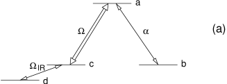
The absorption spectrum of a weak probe field () can be changed by coherently preparing a so-called -system (states , , and of Fig. 1). This can be accomplished by a strong coherent field (with Rabi frequency ) that gives rise to two interfering Stark split absorption lines [2]. When a fourth state is coupled by a weak field with Rabi frequency (from now on referred to as “IR field”) the resulting interaction Hamiltonian reads
| (1) |
Without IR field, the “dark” state is decoupled from the optical fields (). When the system is driven into this state, the pair of fields propagate through the medium unhindered, i.e. the medium is transparent on resonance (broken line in Fig. 2). In case of , nearly coincides with the dark state, thus basically all population collects in ground state .

A perturbation of the dark state by a coherent field does not necessarily lead to the destruction of coherence. However, can dramatically affect the absorption of the weak probe field. The transparency splits in two, and results in a “double dark” resonance, interfering into a very sharp, coherent absorption line in between. Nearly all electrons stay in ground state .
The propagation dynamics of the probe field is described by the susceptibility
| (2) |
where , is the electron density, are the relaxation rates of the respective coherences and , , and , where () is the detuning of the probe (coupling, IR) field to its respective transition. The absorption spectrum of the probe field is shown in Fig. 2, for the IR field on (solid line) and off (broken line)[10]. If the Rabi frequency of the perturbation is weak the sharp additional absorption line of the probe field has approximately Lorentzian line shape with a width of , where is the linewidth of the IR field, and at a frequency of , where is the probe resonance frequency, and the decay from state to . Thus frequency and width of this new resonance can be manipulated by changing detuning and intensity of the IR field.
In a system where all three fields are on resonance and the IR Rabi frequency is very small compared to , the -type absorption profile is nearly undisturbed everywhere except for the resonance region. But where there was transparency before is now a sharp absorption line which splits the transparency in two (see Fig. 2) [10].
Note that if the sharp, new transparency resonance appears near the maximum absorption of the -system (see Fig. 2, dotted line). Thus it is also possible to turn absorption into transparency.
These features make the present system suitable for a novel kind of detector. In the case of , i.e. when all three fields are on resonance, either both the probe and the IR field are absorbed, or none [11]. If the IR field is a long-wavelength infrared field, and the probe field an optical field, the absorption characteristics of the visible probe field on resonance translate into the absorption characteristics of the IR field. However, the scheme can be used in the opposite mode as well: If one detunes the perturbation to , the Stark shifted probe field absorption turns into transmission when the IR field is present. In this case, only one of the fields is absorbed, either the optical probe field or the IR field, but never both. In the following paragraphs only the first setup is closely examined. However, both setups result in similar sensitivity, and there might be cases where the second mode might be more practical [12]. This “frequency translation” can in an obvious way be used not only for detection but also, e.g., for switching, converting, imaging.
It should be mentioned here, that for an ideal setup, i.e., where all three states , , and are stable and all fields are monochromatic, this scheme possesses unlimited sensitivity. In any realistic situation the sensitivity depends on the total ratio of the decoherence, that is, the lifetime of the metastable states, and additional incoherent mechanisms such as phonon scattering, to the strength of the coherent coupling mechanisms.
The sensitivity for such a system can be found through an operator-/C-number Langevin approach, assuming -correlated noise. The strength of the signal is given by the reduction in the probe intensity transmitted when the IR field is turned on:
| (3) |
With that the efficiency reads
| (4) |
where () is the radiative decay along the probe (IR) transition, =1-10meV, the decoherence =1meV on the most critical transition (in this case the transition between states and in Fig. 1a). It turns out that for intraband quantum well systems, the ratio is usually of the order of one. For the Rabi frequency of the probe field meV, i.e., the saturation point, we can reach an efficiency of up to three orders of magnitude between the signal and the IR field. From equating signal to noise, obtained from a somewhat lengthy calculation (see [12]) we find the minimum detectable power of
| (6) | |||||
where is the photon energy of the IR field and the measuring time. For the parameters of the semiconductor example discussed later, with m, GHz this gives the order of 1J/sec for a measuring time of one second. Unity optical density is assumed.
Note that complete transparency is ideal but by no means necessary in order for the detector to perform well: The figure of merit is the factor , which describes effectively the coherence-to-incoherence ratio in the system, as mentioned above.
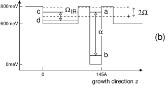
For the solid state realization in semiconductor quantum well systems, eigenstates can be treated in many aspects like atomic states. That is, in Fig. 1b the eigenstates of the uncoupled wells would be analogous to the respective states in Fig. 1a. However, in a double well potential the electrons tunnel through the very thin barrier between the two wells; thus, the states (e.g. and ) mix, split, and are shifted by . Approximately, superposition states of the uncoupled well states emerge. The splitting can be compared with the Stark splitting in atomic states caused by a strong coupling laser field, , like in Fig. 1a. The two resulting resonances (corresponding to states and) also interfere destructively, so that an EIT-like spectral pattern emerges. In this case, however, resonant tunneling and not an external monochromatic field is the coherence generating mechanism. In this case the EIT phenomenon can be viewed as resulting from Fano-type interference. We also note that another degree of freedom can be added to this system (Fig. 1b): If one side (in our case the side of increasing ) is “opened,” i.e. the potential of the right side is lowered, a quasi-continuum of states instead of the discreet eigenstates is found. The magnitude of the Fano term is directly proportional to the square root of the multiplied widths of the excited states and . This term therefore depends strongly on the excited state lifetimes.
The theoretical approach to describing states as well as coupling and dephasing strengths in quantum wells is simple, but gives only an estimate of the order of 10-50% accuracy in energy and coupling strengths. The envelope function of any particular 1-D well geometry can be determined via a transition matrix method in the case of discrete states and borrowing the method of calculating Feshbach resonances (see, e.g., [13]) for quasi-continuous states, where also the emerging finite lifetimes are found. (These states tunnel into the continuum, like the one in Fig. 1b far right, above 600meV.) The dipole element between any two states using envelope functions is found via , where is the electron charge, and the 1-D envelope functions. All emerging parameters can now be plugged into the usual Maxwell-Bloch equations.
The most important phase destroying mechanisms in semiconductor quantum wells include phonons, non-parabolicity, many-body effects, and geometrical imperfections.
The problem we are dealing with is adiabatic and includes no (or nearly no) excited state population. Thus many-body effects can be neglected (see, e.g. [9]). With electrons always having enough time to relax to the bottom of the band before any light induced transitions, non-parabolicity can be neglected as well compared to most other dephasing mechanisms, in particular in GaAs based structures, where the effect of non-parabolicity is very small.
Phonons are strongly frequency and temperature dependent: Since the energy gap between state and the higher lying states is several hundred meV, not even polar optical phonons are playing a big role in population transfer, as it would be the case in a traditional QWIP, where the electrons have to be transported only over a range of few tens of meV. On the other hand, phonons do play a role as dephasing agents. The relevant quantity for both optical and acoustical phonons is the matrix element , where acoustical phonons are proportional to , and polar optical phonons are proportional to , where is the in-plane momentum. The upper limits of acoustical and polar optical phonons (cf. [14]) in this proposed structure are smaller than meV and 0.1meV, respectively.
It thus turns out that the most threatening dephasing mechanism derives from geometrical imperfections, that is, interface roughness scattering: The quantum wells and barriers needed for this kind of device are often only several atomic layers thick. Even in the best molecular beam epitaxy machines that are found today it is impossible to grow the required quantum structures completely smooth. But differences in thickness in the barriers or wells have a relatively strong influence on the energy of and resonances between eigenstates. In the experiments on this subject [7] the coherence decay due to interface roughness is roughly 0.5-1meV.
The rule of thumb, that most incoherent broadening can be somehow mitigated, probably also applies here: Using the spin components of the electronic (or hole) eigenstates should improve the decoherence times considerably, in particular if the two states where decoherence hurts most (tates and in Fig. 1), are spin components of the same electronic eigenstate (for details see [12]).
The simulations shown in Fig. 3 have the parametric values incorporated: Two samples, both without and with additional (i.e. geometric etc.) dephasing, are tested. Both are GaAs/AlxGa1-xAs structures with high- wells for a high offset (800meV) and medium for the shallow well. The emerging offsets and well/barrier widths are as shown in Fig. 1b. The system is modulation-n-doped to provide the necessary ground state population. (Optimal electronic density is assumed which would in practice depend on the number of repetitions of the structure, beam widths etc.) For the simulations GaAs/AlGaAs effective masses of 0.067 electron masses are assumed.
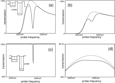
Figs. 3a,b show a structure with short lived excited states (notice the “open” geometry in the inset) and thus large Fano factors, (b) has the dephasing included. The input IR frequency has a width of 10GHz (for all Figs.) and an intensity of 2.5 mW/(10m)2, with a parametric dephasing of 1meV. In Figs. 3c,d the excited states are narrow (no quasi-continuum), and the IR power is 0.1W/(10m)2, with a parametric dephasing of 0.5meV. (This value seems attainable with present day technology, cf. [7]).
It is obvious that this kind of detector is not broadband, like QWIPs with the excited state in the continuum, but rather energy selective. For best results, a frequency filter should be used. On the other hand, comparing the sensitivity estimate (Eq. 6) with an analogous one for a QWIP with comparable coupling strength (which should be only possible with the more restrictive bound-to-bound state QWIPs) we find for the ratio of the minimum detectable powers:
| (7) |
where the decoherence in the QWIP results from the broadening of the lower QWIP state (through phonons, tunneling into continuum).
In conclusion we have demonstrated an example of a new kind of coherence based nonlinear optical process in semiconductor quantum wells. Specifically we have shown how it is possible to use this technique for sensitive photo detection.
We also note that there exists a number of avenues for improvement. A better frequency range for the probe field, e.g. visible or 1.5m, can become accessible by moving the ground state into the valence band. In this case, doping would not be necessary. Further improvement in terms of coherence lifetimes is expected from utilizing the electronic spin states in the conduction band. In this case static or dynamic magnetic fields can be coupled and detected in intraband transitions in the THz range, or polarized electromagnetic fields in interband transitions. The relevant coherence lifetimes are expected to be up to four orders of magnitude higher than for present systems.
We want to thank L. Friedman, M. D. Lukin, R. Soref, G. Sun for stimulating and helpful discussions. SFY would like to thank the Humboldt Foundation for their support.
REFERENCES
- [1]
- [2] K.-J. Boller, A. Imamoğlu, S. Harris, Phys. Rev. Lett. 64, 2593 (1991); for review see S. Harris, Physics Today 50, 7, 36 (1997).
- [3] K. Hakuta, L. Marmet, B. P. Stoicheff, Phys. Rev. Lett. 66, 596 (1991)
- [4] P. R. Hemmer et al., Opt. Lett. 20, 982 (1995); T. T. Grove et al., Opt. Lett. 22, 769 (1997); T. T. Grove et al., Opt. Lett. 22, 1677 (1997).
- [5] M. D. Lukin et al., Phys. Rev. Lett. 79, 2959 (1997).
- [6] K. Hakuta et al., Phys. Rev. Lett. 79, 209 (1997).
- [7] J. Faist et al., Nature 390, 589 (1997); A. Imamoğlu, R. J. Ram, Opt. Lett. 64, 873 (1994); H. Schmidt et al., Appl. Phys. Lett. 70, 3455 (1997).
- [8] In G. B. Serapiglia et al., Phys. Rev. Lett. 84, 1019 (2000) the transparency is not created via resonant tunneling.
- [9] D. E. Nikonov, A. Imamoglu, L. V. Butov, Phys. Rev. Lett. 79, 4633 (1997); D. E. Nikonov, A. Imamoglu, M. O. Scully, Phys. Rev. B 59, 12212 (1999).
- [10] M. D. Lukin et al., Phys. Rev. A 60, 3225 (1999).
- [11] S. Harris, Y. Yamamoto, Phys. Rev. Lett. 81, 3611 (1998).
- [12] S. F. Yelin and P. R. Hemmer, “Sensitivity estimates for a coherence based detector in semiconductor nanostructures” (in preparation).
- [13] H. Friedrich, “Theoretical Atomic Physics,” Springer, Berlin (1998).
- [14] G. Sun, Y. Lu, L. Friedman, R. A. Soref, Phys. Rev. B 57, 6550 (1998); G. Sun, L. Friedman, Phys. Rev. B 53, 3966 (1996).