Schellingstr. 4, D-80799 München, Germany
Applications of Integrated Magnetic Microtraps
Abstract
Lithographically fabricated circuit patterns can provide magnetic guides and microtraps for cold neutral atoms. By combining several such structures on the same ceramic substrate, we have realized the first “atom chips” that permit complex manipulations of ultracold trapped atoms or de Broglie wavepackets. We show how to design magnetic potentials from simple conductor patterns and we describe an efficient trap loading procedure in detail. Applying the design guide, we describe some new microtrap potentials, including a trap which reaches the Lamb-Dicke regime for rubidium atoms in all three dimensions, and a rotatable Ioffe-Pritchard trap, which we also demonstrate experimentally. Finally, we demonstrate a device allowing independent linear positioning of two atomic clouds which are very tightly confined laterally. This device is well suited for the study of one-dimensional collisions.
PACS: 32.80.Pj, 03.75.-b, 03.67.Lx
1 Introduction
Trapped laser cooled atoms are now widely used in atomic physics experiments Ketterle99a . Magnetic traps are particularly versatile, since they can be used for any atomic species possessing a magnetic moment, and provide conservative potentials even for long trapping times. Although the magnetic potential has merely served as a container in most experiments to date, it also provides an excellent means for more complex manipulation of atomic wave packets. In resonator QED experiments Pinkse00 ; Ye99 for example, it can be used to shift a trapped atom into and out of the quantized light field. Quantum computing schemes have been proposed in which a combination of electric and magnetic potentials controls state-dependent collisions in order to entangle atomic qubits Calarco00 . Such complex potentials can be realized when lithographic or other surface-patterning processes are used to produce the field-creating structures on a suitable substrate, now sometimes called an “atom chip”. The use of lithographic, planar conductor patterns for magnetic atom trapping has been proposed as early as 1995 Weinstein95 . However, no successful experiments were carried out at that time due to the difficulty of loading such traps, which have small volumes and are typically located only a few hundred micrometers or less from the substrate surface. This situation changed last year with our demonstration of an efficient loading mechanism for surface traps Reichel99 . It employs a novel mirror-MOT, using a reflecting layer on top of the circuit pattern to realize the laser fields for laser cooling and trapping in close proximity to the surface. With this loading mechanism, integrated traps for cold atoms became experimentally accessible. In the first demonstration of such a trap, the new loading mechanism was employed to fill a miniature quadrupole trap featuring transverse gradients of 1700 Gcm Reichel99 . The trapping potential was created by a lithographically produced, U-shaped conductor in conjunction with an external bias field. In the meantime, the same loading and trapping techniques have also been applied to construct a Ioffe-Pritchard (IP) trap for 7Li atoms Folman00 . The mirror-MOT technique has also proven its usefulness beyond lithographic traps as it was used to fill surface traps of a different type, which result from the combination of permanent surface fields on magnetic tape with an external bias field Rosenbusch00 .
Indeed, lithographic conductors are now increasingly employed to trap, guide and manipulate cold neutral atoms. Parallel conductors have been used to realize atom guides in which atoms are confined in two dimensions and move freely along the third Mueller99 ; Dekker00 . Very recently, more complex conductor patterns were used to realize an atomic conveyer belt, which adiabatically transports atoms and positions them with a precision of the order of m Haensel00a . Moreover, two “beam splitters” have been demonstrated, one which distributes a trapped cloud in a Y-shaped pattern Cassettari00 , and one which splits a guided beam using an X-shaped pattern Mueller00 . Such devices demonstrate the versatility of the new approach. Considering the relative ease of these experiments now that major obstacles have been removed, we foresee a wide variety of applications for lithographic microtraps. In this article, we discuss some key issues of microtrap design and realization. We propose a modular, intuitive approach to the design of complex potentials from a few simple building blocks. In the following sections, we tackle the substrate technology and give a detailed description of the loading procedure. The wide-ranging possibilities offered by simple conductor configurations are illustrated by experimental results of trapping in some fundamental types of potentials which would be very difficult to create by more traditional means. Finally, we demonstrate a linear collider for trapped atoms, which is well suited for the study of one-dimensional collisions.
2 Design of integrated microtraps
In this section we present a method to design a variety of microtraps from simple 2D-conductor configurations which serve as modular building blocks. As central part we investigate the magnetic potential at a perpendicular wire intersection, which can then be used to construct more complex magnetic potentials. Throughout the discussion we will denote the vector normal to the substrate surface, all current carrying wires are contained within the plane at =0.
2.1 2D-quadrupole fields
Ioffe-Pritchard (IP) traps can be regarded as superposition of a two-dimensional quadrupole field for transverse confinement and a longitudinally varying field for confinement along the quadrupole axis. The 2D-quadrupole field can easily be created in the vicinity of a current carrying wire (here along , if its tangential field is compensated at the point by the homogeneous field
| (1) |
(see fig. 1).
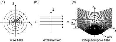
Magnetic traps and waveguides employing this scheme have been realized both with discrete Fortagh98 ; Denschlag99 and with lithographic wires Reichel99 ; Dekker00 ; Folman00 . Furthermore, schemes have been studied that permit the creation of quadrupole guides without the use of external fields (see e.g. Thywissen99 ).
2.2 Modification of the longitudinal potential
The field strength along the longitudinal trap axis can be varied by adding another field to the quadrupole field . The components yield a shift of the trap position along and respectively, whereas the modulus of determines the field strength at the shifted minimum location. Using a linear approximation for the quadrupole field
| (2) | |||||
| (3) |
the total field and the transverse trap position can be expressed to 0 and 1 order, respectively, as
| (4) | |||||
| (5) |
Here signifies the lowest value of the magnetic field within the plane perpendicular to the axis, denotes the corresponding minimum position. According to eq. 4 the transverse field minimum can be approximated by taken at the position of the unshifted quadrupole guide. This method can be used to develop an intuitive understanding of many magnetic potentials that are based on a 2D-quadrupole trap.
2.3 Wire intersection
A high field , i.e. a strong longitudinal potential, may be obtained by a wire that intersects the x axis at right angle.
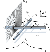
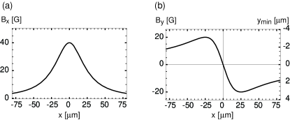
Fig. 2 illustrates the geometry of the wire intersection that will serve as building block for more complicated traps. For demonstration, we choose a current of A which together with a magnetic bias field of G yields a 2D-quadrupole guide above the surface111These parameters are realistic, see Sect. 3.1. At this distance, the current creates a field with components
| (6) | |||||
| (7) | |||||
| (8) |
which are shown in fig. 3.
As the lorentzian shape of suggests, the field contribution of the intersecting wire can be used to create a repulsive potential along the quadrupol axis (Fig. 4 a-c). However, the repulsive character of the crossing current can be converted into an attractive one if a homogeneous bias field is superimposed. In this case, the field along the axis becomes
| (9) |
which exhibits a minimum at . This field configuration thus provides a trapping potential in all three dimensions (fig. 4 d-f). Wires supporting a current flow perpendicular to a quadrupole guide can therefore be used to create repulsive as well as attractive potentials along the trap axis, depending on the strength of the external field .
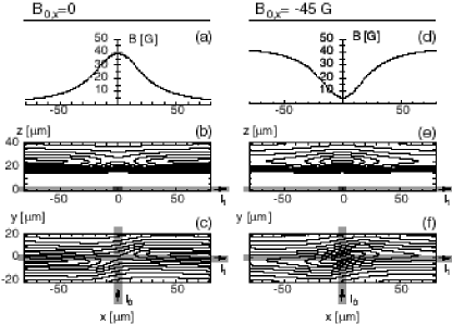
In order to reflect the physical properties of the trapping potentials, each plot in fig. 4 shows the minimum potential value within the plane (a,d) or line (b,c,e,f) that is perpendicular to the visible line or plane.
A detailed look at the potentials in fig. 4 reveals how the minimum position of the trap is displaced by the field component of the crossing current. The approximations in eq. 4 and 5 hold as long as the intersecting current is smaller than the current in the central wire (). Here we have chosen , the approximation therefore predicts to vary according to
| (10) |
as is indicated on the right hand scale of fig. 3 (b). The deviation from the approximated field strength is indeed so small that it is not visible on the scale of the plots (a) and (d) of fig. 4.
2.4 Composing more complex traps
The fields of several intersecting wires can now be added to obtain more complex magnetic potentials. Fig. 5 illustrates the potentials that arise in the vicinity of two parallel wires that intersect the central wire at two points 100 m apart from each other. For the intuitive understanding the field contributions from the two wire can be summed up in order to give the complete longitudinal potential.
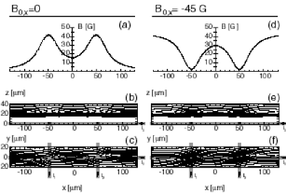
Without external bias field , the field configuration exhibits one IP-trap in the center of the two intersecting wires. Contrary to conventional IP-traps, the field direction in the center does not coincide with the slowest trapping axis: the center field is along , whereas the slow axis is turned by the influence of the vertical field components of the intersecting wires.
If a bias field is applied, two IP-traps form above the intersection points, each slightly displaced by the influence of the opposite wire (see fig. 5 f). In a similar way, a long chain of magnetic traps can be constructed. The magnetic conveyer belt Reichel99 ; Haensel00a can be understood in terms of this design principle. As multiple intersections of the modulating wires cannot be realized in a single-layer substrate, the wires are bent off to avoid the crossing.
2.5 Choosing configuration parameters
The analytical form of the longitudinal trap potential (eq. 4) can be used to design magnetic traps for specific purposes. Here we present an IP trap that is optimized for high longitudinal oscillation frequency. Applying equation 6 to the H-shaped IP trap (fig. 5 d-e), simple calculations show that, for a given height , the longitudinal field curvature is maximized if the intersection points are placed at
| (11) |
from the center.
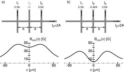
Fig. 6 (a) illustrates that the center field of this wire configuration attains comparably high values. A third current crossing the trap axis in the center of the two parallel wires and in opposite direction can thus be used to further increase the field curvature and to thereby decrease the absolute value of the minimum field strength.
The potential of this optimized four-wire trap is shown in fig. 6 (b). Table 1 lists, for all three eigenaxes, the field curvature, the oscillation frequency and the Lamb-Dicke parameter defined as , where is the recoil frequency for 87Rb. The field curvatures along the eigen-axes all exceed G/cm2, so that 87Rb atoms in the -ground state can be trapped within the Lamb-Dicke regime along all axes.
| Lamb-Dicke | |||
|---|---|---|---|
| dir. | field curvature | osc. freq. | parameter |
| 1 | G/cm2 | 42 kHz | 0.30 |
| 2 | G/cm2 | 42 kHz | 0.30 |
| 3 | G/cm2 | 5.1 kHz | 0.86 |
3 Key techniques of the microtrap experiment
3.1 Substrate technology
A wide variety of micro- and nanofabrication techniques appear suitable for atom chips, including standard microelectronics processes. Microchip materials generally have low outgassing rates, making them suitable for UHV use, although some restrictions arise from the requirement of bakeability. High field gradients and curvatures are among the most attractive features of magnetic microtraps; in order to optimize these features, the atom chip should provide low-resistance conductors suitable for high current densities. Therefore, gold and copper are desirable conductor materials. Finally, the size scale of the structures also enters in determining the most suitable process. Pure lithographic techniques used with sputtered or evaporated metal layers usually limit the maximum layer thickness to a few micrometers. If the scale of the conductor width is rather in the m range, as is the case in all current experiments, an additional electroplating step is helpful to increase the height of the conductor cross section, thereby lowering the resistance. Thin-film hybrid technology is a standard process combining lithography and electroplating. It employs gold conductors on aluminum oxide, aluminum nitride or sapphire substrates. The minimum width of conductors and gaps is typically 10 m. We have chosen this process for our experiments because it fulfills all the cited requirements and because custom-made hybrids are commercially available. A very similar, custom-developed process was used in the atom guiding experiments at Harvard Dekker00 . One interesting alternative is the process used by the Innsbruck group, which uses a uniform gold layer on a gallium arsenide substrate. This custom-made process is more difficult to produce, but has the potential to create smaller structures and leads to a very smooth gold surface.
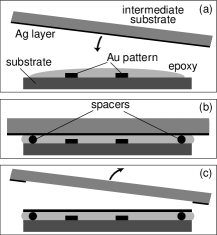
The mirror-MOT requires a reflective substrate surface. As the conductor pattern forms a relief structure on the surface, directly applying a coating to it would lead to a poor mirror with strong diffusion from the conductor edges. We therefore use a simple “replica optics” procedure as described in figure 7 to obtain a flat mirror. The final substrate has the layer structure shown in figure 8. The size of our substrates is . This is large enough even for complicated conductor patterns, but limits the size of the mirror and thus the MOT beam diameter, see section 4. Thin-film hybrid substrates are available in larger sizes, e.g. .
The maximum sustainable current through the lithographic conducters is a key parameter in order to obtain steep traps. The thinnest wires on our hybrid substrates have a cross section of m height and m width. With the literature value of cm for the specific resistance of gold, this leads to a resistance of 3.1 cm and a dissipated power of Wcm at A. Two effects impose limitations on : global heating of the substrate by this considerable total power, and local effects which lead to melting or evaporation of the wire at one specific point. The first limitation can always be alleviated by improving the heat conductivity from the substrate to the reservoir to which it is connected, or, if necessary, by cooling this reservoir (e.g., by using a small liquid nitrogen tank). The second, local effect is characteristic of the microfabrication process and materials and is the one which actually limits .
In our setup, active cooling proved to be unnecessary and the cooling system is most simple. Heat removal from the substrate is ensured by fixing it on a copper block with an UHV-compatible, thermally conductive epoxy resin (Epo-Tek H77). The copper block acts as a heat buffer and is itself connected to the stainless steel vacuum system by copper rods. We have determined the maximum sustainable currents in hybrid wires (m, , length mm) in this assembly. The tests were done in air with the copper block posed on a wooden table and initially at room temperature. We obtained the following result: currents of A could repeatably be applied for one minute; the copper block heated up by about 40 K during that period. At currents above A, some wires blew up, forming m long gaps in the wire. Thus, the highest sustainable current density (at A) was . The calculated magnetic field of a m wide conductor carrying a current of A is 425 G at a distance from the surface and has a gradient of G/cm. Superposing a sufficient longitudinal bias field to suppress Majorana losses (, see e.g. Gov00 ), a Ioffe-Pritchard trap with a transverse oscillation frequency of 270 kHz could be realized for 87Rb atoms. The resulting confinement leads to a Lamb-Dicke parameter of 0.12 with respect to the D2 line, corresponding to a ground state diameter of 60 nm. These surprising figures suggest that traps with exciting new properties may be realized with this simple technique.

3.2 Vacuum system and outgassing issues
The conductors on the substrate are contacted to connector pins by gold wire bonding. This technique, extensively used in microchip packaging, requires no soldering compounds and is therefore well suited for UHV use. However, a special wire bonder is required. Contacting with a silver-filled epoxy is an alternative if a wire bonder is not available Folman00 . Kapton isolated copper wires with matching UHV connectors are used between the connector pins and the vacuum feedthrough.
Considering the quantity of materials employed in vacuo, the final pressure in the system is of interest. Our small-volume vacuum system is pumped by a 25 ls ion pump and a simple titanium sublimator. Both pumps are connected to the glass cell containing the substrate by 35 mm stainless steel tubing, involving several angles between the cell and the pumps. A vacuum meter, which is located about midways between the pumps and the glass cell, indicates a final pressure of mbar typ. after 3 days of baking at C. More importantly, we observe lifetimes in the magnetic trap of s, depending on the Rb pressure. It seems reasonable to expect an order of magnitude gain if a separate MOT chamber is introduced and the pumping speed is improved. Thus, the atom chip materials are compatible with the vacuum level required for evaporative cooling or certain quantum manipulation experiments.
3.3 Detection
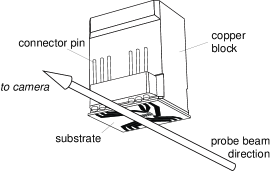
The substrate is mounted upside down in the vacuum chamber, so that atoms are “hanging” below its surface. This enables time-of-flight imaging to measure the velocity distribution. A probe beam for absorption imaging is directed parallel to the surface along the axis (figure 9). The shadow of the atom cloud is imaged onto a 12 bit CCD camera by a multi-element zoom lens. Magnification is limited by the requirement to image the full mm length of the atomic conveyer belt. This in turn sets the resolution to 23 m in object space, limited by the CCD pixel size.
After every absorption image, a reference image is taken without atoms. Dividing the intensities of both images and taking the logarithm yields the optical densities. All images shown in the following section are obtained in this way.
4 The trap loading procedure
One of the key issues of an atom chip experiment is to load cold atoms into microtraps which have much smaller volumes than usual magnetic traps and are located in close proximity to a substrate surface. Our loading scheme relies on a mirror-MOT (Reichel99 , see also Pfau97 ) for preparing cold atoms close to a surface, and on a field switching procedure in the MOT phase (from a “macroscopic” quadrupole field to a “microscopic” one) to achieve reproducible trap loading without the need for precision field alignments. A schematic of the mirror-MOT is shown in fig. 10. Two of the six MOT laser beams are generated by reflection on the mirror, the resulting total light field is identical to that of a standard MOT. The loading procedure has been described in Reichel99 and is summarized in figure 11. We obtain up to atoms trapped in the MOT, limited by the small trapping beam diameter of mm (which is itself limited by the substrate size, as MOT beams are reflected on it), by the total laser power of mW, and by the rubidium pressure. We adjust this pressure to rather low values, i.e. on the same order as the mbar background pressure, in order to achieve long magnetic trapping times. A dispenser mounted above the substrate serves as thermal rubidium source and allows for relatively fast pressure adjustments.

5 Demonstration of fundamental microtrap potentials
In Sect. 2 we have described how simple conductor patterns can be used as “modules”, which can be combined to form complex potentials. Some of these modules create potentials which are useful by themselves, and we start our presentation of experimental results with two of these: First, a conductor cross is used to create an IP trap in which the long axis and the atomic polarization can be rotated about the conductor intersection. In the second experiment, a long, “Z” shaped conductor (which approximates the “H” shape of Sect. 2) creates a very elongated IP trap, in which the atoms are strongly confined transversally and move almost freely about mm along the long axis.
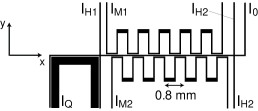
All experiments are carried out with the conductor pattern of figure 12Reichel99 ; Haensel00a . The variety of basic conductor shapes which it contains makes it versatile enough for a large number of different experiments.
5.1 Rotatable IP trap
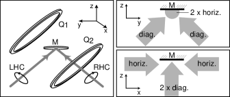
It was shown in Sect. 2.3 that two crossing conductors carrying different currents create an IP trap when a suitably oriented bias field is superposed. As the conductor pattern is symmetric, different orientations of the long trap axis can be obtained by exchanging the currents and bias field components (upper part of fig. 13). By smoothly varying the currents and bias field components, the long axis may even be turned continuously222When a pure symmetric conductor cross is used, the potential passes through a quadrupole ring shape for the intermediate situation . However, the additional field components introduced by the bent conductors in our experiment lift this degeneracy, so that the trap remains of the IP type during the whole rotation. by 90∘. We use the intersection of and to create a trap of this type (cf. Fig. 12). The lower part of Fig. 13 shows absorption images of the atoms in such a trap for different orientations of the long axis. The right image shows a trap that was obtained by turning as described above. The trap parameters are A, A, G, G, leading to curvatures and to oscillation frequencies Hz. The ability to align the magnetic polarization of the trapped cloud can be essential when a well-defined coupling to a polarized external field is required, such as the evanescent light field of a whispering gallery mode in a high-finesse microsphere resonator Treussart94 ; Vernooy98 .

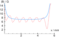
5.2 Highly elongated IP trap
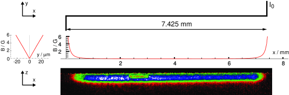
Potentials that restrict the atomic motion to one dimension are interesting from both the theoretical and the experimental point of view. The scattering properties of cold atoms Weiner99 change dramatically in reduced dimensionality Olshanii98 ; Mandonnet00 ; when the transverse level spacing exceeds the thermal energy of the atoms, one may construct single-mode de Broglie waveguides Thywissen99 , which are one of the building blocks of future trapped-atom interferometers Adams94 . With lithographic magnetic traps, the construction of such waveguide potentials is straightforward since they derive directly from the fundamental element of a single wire with a perpendicular bias field. As shown in Sect. 3.1, our m thin-film conductors permit transverse level spacings of several 100 kHz for Rb atoms. In the pattern of fig. 12, may be used to create an IP trap of this kind, with steep transversal confinement and an almost box-like longitudinal potential created by the bent parts of the conductor. The width of this conductor is m, but in our experiment the transverse curvature is not yet limited by this wire width. In fact, our modest bias coil systems permits a maximum bias field of only G, so that we cannot as yet exploit the full potential of the conductor pattern. At G, the potential of fig. 14 (center) is obtained. The bias field in this example is uniquely generated by the wire sections which are parallel to the axis, and is correspondingly small (0.01 G in the center). However, an external bias field along the axis is compatible with this potential (see next section). Figure 14 shows an absorption image in the potential described above. In this guide, the atoms experience a transverse field gradient of 3000 Gcm, which allows for trapping frequencies up to 10 kHz, depending on the bias field along the trap axis. (Cf. Sect. 3.1 for the choice of the bias field).
6 Linear cold atom collider
Highly elongated, cigar-shaped potentials like the one of fig. 14 have been considered by theorists in the context of one-dimensional scattering of cold atoms, for which surprising properties have been predicted Olshanii98 ; Mandonnet00 . Cold collisions are also a key ingredient of quantum computing schemes with cold atoms Calarco00 . An ideal situation consists of two atoms or atom clouds strongly confined in two dimensions and freely moving along the third, approaching each other with well-defined initial momentum. Such a situation can be realized in the device we demonstrate in this section. It separates two samples of cold atoms so that they move to the ends of the cigar-shaped potential, and then releases them with opposite linear velocities (while maintaining the transverse confinement), so that they meet in the center of the trap. Although our atomic samples, which have not been evaporatively cooled, are still too hot to enter into the one-dimensional regime, this device is a good illustration of the atom manipulation capabilities offered by lithographic microtraps.
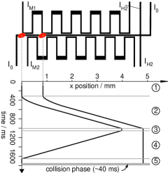
The device is based upon the atomic conveyer belt which we recently demonstrated Haensel00a , and the potential of which is which is described in Reichel99 . It enables us to cut a long Ioffe trap into a chain of small, tightly confined Ioffe traps, which can be moved along the central wire axis by smoothly alternating the current flowing through the additional wires M1 and M2 (see fig. 15). To separate two atom clouds widely, we load the two leftmost magnetic conveyer belt potentials and bring them into the collider starting point by the procedure described in fig. 15. Next, we abruptly turn off all wire currents except the central one. As described in Sect. 5, the atoms are now almost free along the long axis and tightly confined in transverse direction. Due to the steep increase of the longitudinal potential at its ends, the atoms are accelerated towards each other. Fig. 17 shows the center of mass (CM) position of both clouds before and after their encounter. The dashed lines are linear fits on the last ten points before the clouds overlap. As the kinetic energy of the clouds is much larger than the transverse level spacing, collisions will lead to a deviation from the fit line of the CM positions after the encounter due to the redistribution of kinetic energy into the transverse degrees of freedom. In the present demonstration experiment, which was not optimized for high densities, the 10 ms encounter does not lead to a significant effect of collisions. Nevertheless it represents probably the most complex manipulation of atom clouds that has been carried out in magnetic traps, and thus shows the power of the new and flexible manipulation techniques which lithographic microtraps have to offer.

7 Outlook
The results we have presented show that lithographic microtraps offer truly intriguing possibilities for the controlled manipulation of cold atoms. Multiple atom samples can be moved independently in close proximity to a surface while remaining tightly confined. Complicated potentials can easily be built from simple elements such as the wire cross. A logical next step will be to evaporatively cool the atoms in such a trap, a task for which microtraps are well suited due to the high compression which they allow one to achieve. If Bose condensation, or indeed preferential population of any single vibrational level can be achieved, a host of novel applications becomes accessible, ranging from trapped-atom interferometry to quantum gate operations employing controlled collisions.
References
- (1) See for example W. Ketterle, D. S. Durfee, and D. M. Stamper-Kurn, in Proceedings of the International Scool of Physics “Enrico Fermi”, edited by M. Inguscio, S. Stringari, and C. Wieman, cond-mat/9904034 (1999).
- (2) P. W. H. Pinkse, T. Fischer, P. Maunz, and G. Rempe, Nature 404, 365 (2000).
- (3) J. Ye, D. W. Vernooy, and H. J. Kimble, Phys. Rev. Lett. 83, 4987 (1999).
- (4) T. Calarco, E. A. Hinds, D. Jaksch, J. Schmiedmayer, J. I. Cirac, and P. Zoller, Phys. Rev. A 61, 022304 (2000).
- (5) J. D. Weinstein and K. G. Libbrecht, Phys. Rev. A 52, 4004 (1995).
- (6) J. Reichel, W. Hänsel, and T. W. Hänsch, Phys. Rev. Lett. 83, 3398 (1999).
- (7) R. Folman, P. Krüger, D. Cassettari, B. Hessmo, T. Maier, and J. Schmiedmayer, Phys. Rev. Lett. 84, 4749 (2000).
- (8) P. Rosenbusch, B. V. Hall, I. G. Hughes, C. V. Saba, and E. A. Hinds, Phys. Rev. A 61, 031404(R) (2000).
- (9) D. Müller, D. Z. Anderson, R. J. Grow, P. D. D. Schwindt, and E. A. Cornell, Phys. Rev. Lett. 83, 5194 (1999).
- (10) N. H. Dekker, C. S. Lee, V. Lorent, J. H. Thywissen, S. P. Smith, M. Drndić, R. M. Westervelt, and M. Prentiss, Phys. Rev. Lett. 84, 1124 (2000).
- (11) W. Hänsel, J. Reichel, P. Hommelhoff, and T. W. Hänsch, quant-ph/0008111 (2000).
- (12) D. Cassettari, B. Hessmo, R. Folman, T. Maier, and J. Schmiedmayer, quant-ph/0003135 (2000).
- (13) D. Müller, E. A. Cornell, M. Prevedelli, P. D. D. Schwindt, A. Zozulya, and D. Z. Anderson, physics/0003091 (2000).
- (14) J. Fortagh, A. Grossmann, C. Zimmermann, and T. W. Hänsch, Phys. Rev. Lett. 81, 5310 (1998).
- (15) J. Denschlag, D. Cassettari, and J. Schmiedmayer, Phys. Rev. Lett. 82, 2014 (1999).
- (16) J. H. Thywissen, M. Olshanii, G. Zabow, M. Drndić, K. S. Johnson, R. M. Westervelt, and M. Prentiss, Eur. Phys. J. D 7, 361 (1999).
- (17) S. Gov, S. Shtrikman, and H. Thomas, J. Appl. Phys. D 87, 3989 (2000).
- (18) T. Pfau and J. Mlynek, ”OSA Trends in Optics and Photonics” 7, 33 (1997).
- (19) F. Treussart, J. Hare, L. Collot, V. Lefèvre, D. S. Weiss, V. Sandoghdar, J. M. Raimond, and S. Haroche, Optics Lett. 19, 1651 (1994).
- (20) D. W. Vernooy, A. Furusawa, N. P. Georgiades, V. S. Ilchenko, and H. J. Kimble, Phys. Rev. A 57, R2293 (1998).
- (21) J. Weiner, Rev. Mod. Phys. 71, 1 (1999).
- (22) M. Olshanii, Phys. Rev. Lett. 81, 938 (1998).
- (23) E. Mandonnet, A. Minguzzi, R. Dum, I. Carusotto, Y. Castin, and J. Dalibard, Eur. Phys. J. D 10, 9 (2000).
- (24) C. S. Adams, M. Sigel, and J. Mlynek, Phys. Rep. 240, 143 (1994).