DESY 98-054 ISSN 0418-9833
May 1998
Revised December 1998
The Electronics of the H1 Lead/Scintillating-Fibre Calorimeters
H1 SpaCal Group
Abstract:
The electronic system developed for the SpaCal lead/scintillating-fibre calorimeters of the H1 detector in operation at the HERA ep collider is described in detail and the performance achieved during H1 data-taking is presented. The 10 MHz bunch crossing rate of HERA puts severe constraints on the requirements of the electronics. The energy and time readout are performed respectively with a 14-bit dynamic range and with a resolution of 0.4 ns. The trigger branch consists of a nanosecond-resolution calorimetric time-of-flight for background rejection and an electron trigger based on analog ‘sliding windows’. The on-line background rejection currently achieved is 106. The electron trigger allows a low energy trigger threshold to be set at 0.50 0.08 (RMS) GeV with an efficiency 99.9. The energy and time performance of the readout and trigger electronics is based on a newly-developed low noise (0.4 MeV) wideband (200 MHz) preamplifier located at the output of the photomultipliers which are used for the fibre light readout in the 1 Tesla magnetic field of H1.
Submitted to Nuclear Instruments and Methods A
H1 SpaCal Group
R.-D. Appuhn6, C. Arndt6, E. Barrelet16, R. Barschke6, U. Bassler16, F. Blouzon16, V. Boudry15, F. Brasse6, Ph. Bruel15, D. Bruncko9, R. Buchholz6, B. Cahan5, S. Chechelnitski13, B. Claxton2, G. Cozzika5,∗, J. Cvach17, S. Dagoret-Campagne16, W.D. Dau8, H. Deckers4, T. Deckers4, F. Descamps16,α, M. Dirkmann4, J. Dowdell2, C. Drancourt15, O. Durant16, V. Efremenko13, E. Eisenhandler10, A.N. Eliseev14, G. Falley6, J. Ferencei9, M. Fleischer4, B. Fominykh13, K. Gadow6, U. Goerlach6,β, L.A. Gorbov14, I. Gorelov13, M. Grewe4, L. Hajduk3, I. Herynek17, J. Hladký17, M. Hütte4, H. Hutter4, M. Janata17, W. Janczur3, J. Janoth7, L. Jönsson11, I. Kacl17, H. Kolanoski4, V. Korbel6, F. Kriváň9, D. Lacour16, B. Laforge5, F. Lamarche15 M.P.J. Landon10, J.-F. Laporte5, H. Lebollo16, A. Le Coguie5, F. Lehner6, R. Maraček9, P. Matricon15, K. Meier7, A. Meyer6, A. Migliori15, F. Moreau15, G. Müller6, P. Murín9, V. Nagovizin13, T.C. Nicholls1, D. Ozerov13, J.-P. Passerieux5, E. Perez5, J.P. Pharabod15, R. Pöschl4, Ch. Renard15, A. Rostovtsev13, C. Royon5, K. Rybicki3, S. Schleif7, K. Schmitt7, A. Schuhmacher4, A. Semenov13, V. Shekelyan13, Y. Sirois15, P.A. Smirnov14,d, V. Solochenko13, J. Špalek9, S. Spielmann15, H. Steiner6,γ, A. Stellberger7, J. Stiewe7, M. Taševský18, V. Tchernyshov13, K. Thiele6, E. Tzamariudaki6, S. Valkár18, C. Vallée12, A. Vallereau16, D. VanDenPlas15, G. Villet5, K. Wacker4, A. Walther4, M. Weber7, D. Wegener4, T. Wenk4, J. Žáček18, A. Zhokin13, P. Zini16 and K. Zuber4
School of Physics and Space Research, University of Birmingham,
Birmingham, UKa
Electronics Division, Rutherford Appleton Laboratory,
Chilton, Didcot, UK a
Institute for Nuclear Physics,
Cracow, Poland b
Institut für Physik, Universität Dortmund, Dortmund,
Germany c
DSM/DAPNIA, CEA/Saclay, Gif-sur-Yvette, France
DESY, Hamburg, Germany c
Institut für Hochenergiephysik, Universität Heidelberg,
Heidelberg, Germany c
Institut für Reine und Angewandte Kernphysik, Universität Kiel,
Kiel, Germany c
Institute of Experimental Physics, Slovak Academy of
Sciences, Košice, Slovak Republic d
10 Queen Mary and Westfield College, London, UK a
11 Physics Department, University of Lund,
Sweden e
12 CPPM, Université d’Aix-Marseille II,IN2P3-CNRS,Marseille,France
13 Institute for Theoretical and Experimental Physics,
Moscow, Russia f
14 Lebedev Physical Institute,
Moscow, Russia
15 LPNHE, Ecole Polytechnique, IN2P3-CNRS,
Palaiseau, France
16 LPNHE, Universités Paris VI and VII, IN2P3-CNRS,
Paris, France
17 Institute of Physics, Czech Academy of
Sciences, Prague, Czech Republic d,g
18 Nuclear Center, Charles University,
Prague, Czech Republic d,g
α now at ILL, Grenoble, France
β now at CRN, Université de Strasbourg, IN2P3-CNRS, Strasbourg,
France
γ permanent address: LBL, University of California, Berkeley,
USA
∗ Corresponding author. Tel.: +33 1 6908 2583,fax: +33 1 6908 6428,
e-mail: cozzika@hep.saclay.cea.fr.
a Supported by the UK Particle Physics and Astronomy Research Council, and formerly by the UK Science and Engineering Research Council.
b Partially supported by the Polish State Committee for Scientific Research, grant no. 115/E-343/SPUB/P03/002/97.
cSupported by the Bundesministerium für Forschung und Technologie, Germany under contract numbers 6DO57I, 6HH27I, 6HD27I and 6KI17P.
d Supported by the Deutsche Forschungsgemeinschaft.
e Supported by the Swedish Natural Science Council.
f Supported by INTAS-International Association for the Promotion of Cooperation with Scientists from Independent States of the Former Soviet Union under Co-operation Agreement INTAS-93-0044.
g Supported by GA ČR, grant no. 202/93/2423, GA AV ČR, grant no. 19095 and GA UK, grant no. 342.
1 Introduction
The H1 detector has been in operation at the HERA ep collider at DESY since 1992. Electrons of 27.5 GeV collide head-on with protons of 820 GeV at a 10 MHz bunch crossing rate. During the HERA winter shutdown 1994-1995, the H1 collaboration upgraded the backward part111Backward refers to the electron direction. of its detector in order to extend deep inelastic ep scattering measurements in the low Q2 ( 1 GeV2) and low Bjorken x ( 10-5) kinematic range. This upgrade program [1] was centred on the construction of two calorimeters (electromagnetic [2, 3] and hadronic [4] wheels) which are based on the lead/scintillating-fibre (SpaCal) technology. In this paper we describe the electronics associated with both calorimeters and present the performance achieved during normal data taking [5].
The major improvements related to the electronics, compared to the previous backward detector [6], concern the physics trigger and the on-line background rejection. The study of low-x deep inelastic scattering makes it necessary to measure the scattered electron down to very low energies at the level of 1-2 GeV whereas incident electrons have 27.5 GeV. A first requirement for the backward physics trigger is the ability to run with a threshold value of 12 GeV. A second requirement for the physics trigger is related to the spatial detection uniformity of this calorimeter, which has a mean value of 2 [7], an important feature that must be preserved at the trigger level. This has led to the construction of a trigger based on ‘sliding’ analog sums which enable recovery of the full deposited energy, regardless of the impact point of the particle.
The purpose of the on-line selection mentioned above is to reject background events induced by collisions between the proton beam (820 GeV) and residual molecules of gas present in the beam pipe upstream of the H1 detector. The rate of these collisions (20 kHz) is a huge source of background triggers which must be reduced by a factor of 104 ; the physics trigger rate, including photoproduction, is of the order of 20 Hz. The required background suppression is achieved by exploiting the path length difference between upstream proton background and physics energy depositions. The front face of the electromagnetic calorimeter is located at m (2.0 m for the hadronic part) from the interaction point, thereby giving rise to a time-of-flight difference of 9 (12) ns for the e.m. (hadronic) calorimeter. An on-line time-of-flight (ToF) selection, at the nanosecond level, by a SpaCal calorimeter is possible due to its intrinsic low jitter (0.35 ns) [8]. In contrast, in the previous calorimeter, out-of-time background event rejection was maintained using signals from an external set of scintillation counters.
In the following section, the general layout of the SpaCal electronics is introduced, while sections 3-7 are dedicated to the detailed description of each of the major components.
2 Main features of the H1 SpaCal electronics
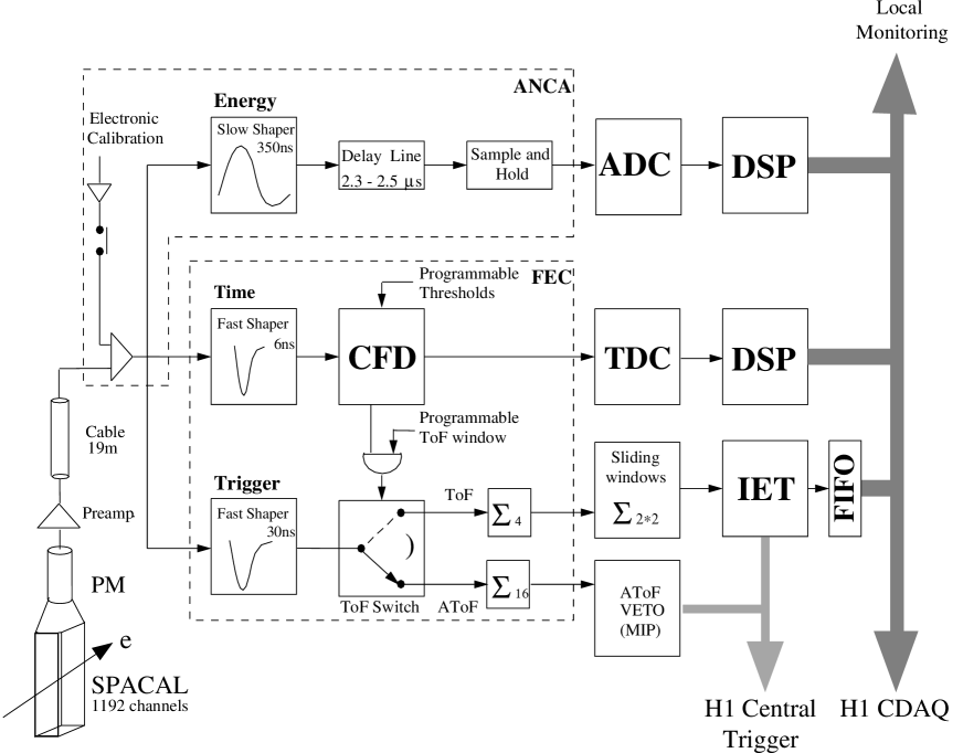
Fig.1 shows the electronics associated with the 1192 channels of the electromagnetic calorimeter. Except for the electron trigger, the same electronics is also used for the 136 channels of the hadronic detector, so only minor differences will be mentioned when necessary, the electronics description always referring to the electromagnetic wheel.
The basis of the improvement discussed in the introduction is a very low-noise wideband readout of the SpaCal light, achieved by a combination of a photomultiplier and a charge preamplifier. The fiber light is read out by fine-mesh Hamamatsu R5505 phototubes (R2490-05 for the hadronic section) which provide a gain of 104 (2 104 for the hadronic section) in the 1 Tesla magnetic field of H1. The detailed characteristics and performance of these photomultipliers are given in references [3, 9, 10]. In order to transmit the photomultiplier pulses to the next stages of the electronics with the best signal to noise ratio, a charge preamplification is performed at the anode output of the phototube. The wideband preamplification associated with the photomultiplier tube is described in the next section, where it is shown that a dynamic range greater than 17 bits at a frequency of 50 MHz is achievable.
As shown in Fig. 1, at the receiver end of the 19 m long 50 transmission cables the pulses are fed into three parallel signal processing chains, which are:
-
•
The energy readout branch described in Sect. 4,
-
•
The timing branch (Sect. 5); as shown in Fig.1, the constant-fraction discriminator (CFD) output of the timing branch is on one hand digitized by a TDC system (Sect. 6) and, on the other hand, used in coincidence with a programmable gate for the on-line time selection of the physics events. This function as well as the two fast shapers and the analog sums ( and ) are performed on the calorimetric ToF board described in Sect. 5.
-
•
The trigger branch (section 7) which includes the level-1 physics trigger mentioned in the introduction, and the total energy Etot first level triggers for physics events as well as for background collisions; the latter are used as vetoes for other H1 triggers.
The three branches are characterized by different time constants, as can be seen in Fig. 1 where peaking-time values are indicated. For on-line background rejection (timing branch), the short time-constant enables the high frequency information of the pulses to be recovered. For the trigger branch, the shaping is chosen in order to get the minimum time occupancy corresponding to the period (96 ns) of the HERA machine clock. For the energy readout branch, the time occupancy per channel due to the 20 KHz background rate allows a longer shaping time compared to the trigger branch.
Part of the electronics (the ANCA and FEC boards of Fig.1) is located close to the iron yoke of the H1 detector in analog boxes designed for optimal shielding and access. Each analog box contains 8 pairs of energy read-out/calorimetric-ToF boards. The electronics of the trigger elements, and the TDC and ADC systems are located 20 m further away, in the main H1 electronics trailer.
3 Preamplification
Usually, a photomultiplier is read out by connecting a matched resistor Rm at the end of a transmission cable. With this configuration, the transimpedance gain:
| (1) |
is constant up to frequencies where ; is the capacitance of the last dynode-anode of the phototube and is the stray capacitance. is the voltage measured across the resistor and the current pulse delivered by the photomultiplier. By using such a readout, it is implicitly assumed that the photomultiplier gain (10) ensures a high signal-to-noise ratio, independent of the signal processing performed in the next stages of the electronics ; here noise means the pickup noise which is added to the signal through the transmission line, the current noise contribution of the dark current being negligible.
However, in our present application the lower gain (104) [10] of the fine-mesh phototubes inside the H1 magnetic field does not ensure such a high signal-to-noise ratio. Therefore it is necessary to preamplify the charge of the current pulse222SpaCal pulses have a rise time of 5 ns and decay with a time constant of 3 ns. = delivered by the photomultiplier (see Fig. 2), using the dynode-anode capacitance as the integrating capacitor. The step voltage decays according to the time constant =, where the mean value of has been set to 180 ns ( = 12 k, ) in order to avoid saturation of the electronics by pile-up effects; this time constant varies from channel to channel (20 maximum) due to the variation of the geometrical capacitance value of the phototube. For the hadronic calorimeter, the fine-mesh phototubes R2490-05 have a larger capacitance value ( 50 pF), so has been chosen equal to 3.3 k.
The two emitter-follower transistors (see Fig. 2) drive the voltage into the transmission cable which is matched at both ends; matching at the emitter side reduces to a negligible level reflected pulses due to residual mismatching at the receiver end. For a background event, such delayed pulses (about two bunch-crossing later) could lead to wrong low-energy physics triggers.
The transimpedance gain of the arrangement of Fig. 2 is given by:
| (2) |
with the complex frequency. In this expression, the higher poles corresponding to the transition frequency (5 GHz) of the transistors (Philips BFQ23) are neglected and a unit voltage gain for both transistors is assumed. Comparing this transimpedance gain with the one provided by the usual readout discussed above, (Eq. 1), we find that, for = 50 , over the wide frequency range MHz.
There are two reasons to use such a preamplifier instead of a conventional charge preamplifier with a feedback capacitor :
-
•
For an energy deposit of 30 GeV inside a SpaCal tower, we already achieve a step voltage amplitude 333Voltage range delivered by the preamplifier is 4 V. (a light yield of 1 photoelectron per MeV deposited energy is assumed) of 3.2 V. So there is no need to increase the gain by using a smaller integrating capacitor,
-
•
With a feedback charge preamplifier, the rise-time of the output pulse is related to the transimpedance of the input transistor and to the total input capacitor. As these two quantities are channel dependent, the use of a feedback charge preamplifier would have introduced timing performance variations, an undesirable feature for the calorimetric ToF function.
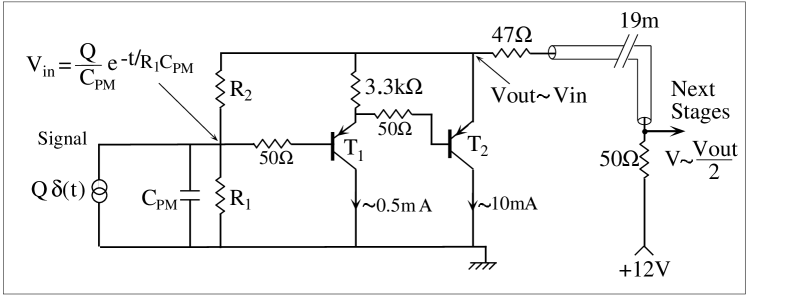
A drawback of the arrangement of Fig. 2 is the gain dependence on the value of , an undesirable feature which is usually removed in a conventional charge preamplifier by knowledge of the value of . However, with phototubes this gain dependence is compensated when the amplification gain of the phototubes is tuned by balancing their response in terms of energy.
The noise contribution introduced by this preamplification is discussed below in order to show that, in terms of energy, it is below 1 MeV. The noise spectral density at the output of the second transistor (Fig. 2) is given by the following expression:
| (3) |
where stands for addition in quadrature ; and are series and parallel noise generators respectively, the impedance given by equation 2.
The series noise generator is equal to:
| (4) |
where 10 is the base spreading resistor of the transistor and () the transconductance of the transistor (). As the collector current of T1 is equal to 0.5 mA, the term amounts to 25 while the contribution 1 ( 10 mA) from T2 is negligible. With these values of and , the series noise spectral density 0.75 nV/.
The parallel noise generator is equal to:
| (5) |
where and (1.8 k) are the resistors of the voltage divider (Fig. 2) and the shot noise of the base current of the transistor T1; 15 A, the current gain being equal to 30 for the BFQ23 transistor. With these values, it is found that 3.86 pA/, where the dominant contribution is provided by the resistor ; in equation (5), we have neglected the noise contribution of the transistor T2.
From equation (3), using the above values for and , it can be seen that series and parallel noise contribute equally at a frequency 5 MHz, the parallel noise dominating at lower frequencies. The noise contributions can be expressed in terms of equivalent noise charge () for the three shapers of the next stages (see Fig. 1) by the usual equation (ref.[11]):
| (6) |
is the maximum of the preamplifier and filter response to a current pulse , and are the series and parallel noise integrals. The values of , and vary according to the shaping performed in the next stages, which can be approximated by:
-
•
(CR)(RC) with CR3 ns for the timing trigger,
-
•
(CR)(RC)3 with RC = 10 ns for the electron trigger branch, and
-
•
(CR)(RC) with RC = 180 ns for the energy readout.
It should be noted that equation(6) is valid for the trigger shapers because the approximate expression (equation 2) can be used (RC). For the readout branch, this approximation does not hold but the formula is still valid provided the transfer function of a (CR)2(RC) shaper is used for the computation of and , the second pole being the one of the charge preamplifier; the values of , and can be found in reference ([12]).
| Electronics | Shaper | Series | Parallel | Total | |||
|---|---|---|---|---|---|---|---|
| Branch | (=RC) | ( (RMS)) | ( (RMS)) | () | |||
| Timing | (CR)(RC) | 0.367 | 1/8 | 1/8 | 1120 | 1270 | 0.17 |
| Trigger | 3 ns | ||||||
| Electron | (CR)(RC)3 | 0.224 | 1/64 | 5/64 | 390 | 2990 | 0.3 |
| Trigger | ns | ||||||
| Energy | (CR)2(RC) | 0.23 | 1/8 | 1/32 | 255 | 7790 | 0.78 |
| Readout | ns |
The noise contributions of the preamplifier for the three shapers are summarized in table (1). From these values, one can conclude that:
-
•
The noise is lower than 1 MeV for both types of shapers
-
•
The achievable dynamic ranges for the energy readout and timing trigger are greater than 15 and 17 bits respectively. It is shown in the next sections that current performance achieved in the H1 experiment are 14 and 15 bits respectively.
4 The energy read-out chain
The energy read-out is performed by 87 electronic boards which process 16 SpaCal channels each. As indicated in Fig. 3 these boards (labelled ANCA in Fig. 1) supply the voltage of the preamplifiers and the impedance termination of the 50 cables. The output of the unit-gain Analog Devices AD 811 amplifier is sent in parallel to the calorimetric ToF board and to the signal processing chain which consists of:
-
•
A (CR)(RC) filter with a time constant = 180 ns. As the mean value of the pole of the preamplifier R1Cpm is 180 ns this filtering is equivalent to a (CR)2 RC shaper, providing bipolar output pulses as shown in Fig. 3. This bipolar shaping was chosen so as to minimize energy pile-up effects for the detector channels close to the beam-pipe.
-
•
A delay line which has been custom built [13] and housed in a shield against the stray field ( 100 Gauss) present close to the iron yoke. Special care was taken in its design in order to reduce to a negligible level parasitic oscillations which can occur before and after the pulse. A fine adjustment of the delay between 2.3 and 2.5 s in steps of 20 ns, set once by jumpers, enables alignment of the peak position of the bipolar pulse with respect to the L1keep signal sent by the H1 first level (L1) trigger. This peak position is measured to an accuracy of 1 ns by the electronics calibration described below.
-
•
The sample and hold S/H (Fig. 3) which stores the value of the signal when an L1keep signal is received. The control switches are based on the same principle as those used in the H1 liquid argon electronics [14] in order to use the same sequencer, but the bandwidth has been increased significantly to deal with the faster SpaCal signals.
The readout of the stored amplitudes by the S/H module uses the same multiplexing, dual output gain (1 and 4), ADC and DSP electronics as for the H1 liquid argon calorimeter (see ref. [15, 16]); the pedestal subtraction, zero suppression and gain selection are performed by the DSP. The dual-gain system was chosen so that the effective dynamic range is 14 bits with a 12 bit ADC. A single coefficient giving the ratio of these two gains is necessary for the 128 channels of one analog box and is known to better than 10-3.
Checks, linearity measurement and delay calibration of the bipolar pulses are performed by electronic pulses fed into the inverting input of the gain-1 AD811 amplifier (Fig. 3). Square voltage pulses received by the generator modules (Fig. 3 ) are provided by the calibration system developed for the H1 liquid argon calorimeter [17]. In a generator module, which drives 8 readout channels, the square pulse is derived by a (CR) of 180 ns in order to simulate SpaCal pulses. The gain-8 (Fig. 3) is necessary to cover the full 4-Volt dynamic range but introduces a total coherent noise of 12 MeV on the 8 readout channels. During normal data-taking, the output of the generator module is disconnected by a relay in order to restore the minimum noise configuration and to minimize high frequency cross-talk (3.5% at 100 MHz).
The integral linearity of the full electronics chain has been found to be of the order of 1. As can be seen in Fig. 3, electronic pulses are also useful for checking the trigger branches. However, for the time calibration of calorimetric ToF boards (sect.5), the square-pulse generator of the liquid argon calorimeter is replaced by a commercial product, HP 8082A, which simulates better the fast rising-edge of the SpaCal pulses. The drawback is that the time calibration procedure is only semi-automatic because the HP 8082A output pulse, which is split passively into 16 pulses, is only capable of driving the 128 channels of one analog box.
5 The calorimetric ToF card
The purpose of this board, labelled FEC in Fig. 1 (for Front End Card), is to perform channel by channel:
-
•
The on-line timing selection of physics events and the rejection of the proton background originating upstream of the beam interaction point,
-
•
The shaping and analog summation of the pulses provided to the electron () and background veto () trigger electronics (Fig. 1).
The inputs to this board are the 16 analog pulses supplied by the preamplifiers, via the energy read-out card and the HERA clock. The outputs provided are five analog sums ( and ) for the electron and total energy triggers and 16 differential signals (CFD outputs) which are sent to the TDC system.
In the timing branch (Fig. 1), the pole of the preamplifier is removed by pole-zero compensation (PZC, zero=225 ns and pole3 ns). In order to prevent CFD oscillations, the time constant of the zero (225 ns) is chosen slightly larger than the expected maximum value of the preamplifier decay time .
The output signals of the CFD are fed in parallel into the TDC system (Sect.6) and the ToF switch. By default the switches are positioned such that shaped pulses of the trigger branch are fed into the AToF (for Anti ToF,i.e. out of time with respect to the beam interaction) branch. The switching to a ToF position requires that the leading edge of the CFD output pulse occurs in a time range, called ToF window, covering the energy deposition time of the physics events. The default position AToF is automatically restored 150 ns after the AToFToF switching. The ToF window is a gate derived for each bunch-crossing from the HERA clock. In order to take into account, channel by channel, transit-time differences of SpaCal pulses and the HERA clock distribution in the boards, the ToF window position is individually tunable by a programmable delay-line (AD9500 chip). The rear edge of the ToF window is also derived from the HERA clock and is tunable by a programmable delay-line which is, for simplicity, common to the 16 channels of a board. This implies that ToF window widths vary from channel to channel, an effect which is taken into account during time calibration procedures. The 8-bit-word programmable delay lines of the ToF windows cover a 70 ns delay range in 270 ps steps of the Programmable Delay Line (PDL).
In the following a more detailed description of the the constant-fraction discriminator, the trigger shaping, and the on-line time selection switches is given.
-
•
The CFD circuit, based on the AD96687 comparator chip, runs in ARC (Amplitude Risetime Compensated) mode with a constant fraction of 20 and a delay of 4 ns. No amplitude validation is done in order to perform the on-line fast switching (Fig.1) within 5 ns; this implies setting the CFD threshold above the noise, as shown below. This voltage threshold is tunable by an 8-bit programmable DAC in the range from -50 mV up to +10 mV in V steps.
-
•
In the trigger branch, the SpaCal pulse is shaped by a (CR)(RC)3 amplifier after PZC (zero=225ns). The unipolar shaped pulse has a typical rise time of 20 ns and returns to the base line, at a level of 1, within 120 ns. The three integrations of the shaper provide the 5 ns delay necessary for setting the switches (Fig. 1).
-
•
The trigger pulse is fed into a pair of switches, one for the AToF line and the other for the ToF one. These switches consist of two BSS83 transistors (Philips) chosen for their intrinsic delay of 4 ns with a small jitter of 0.5 ns. The two-transistor configuration suppresses fully the spike (ref. [18]) induced by the switching.
As explained above, during normal data-taking, these switches are activated (free position) by the timing of the energy deposition. For calibration purposes, the switch states can be downloaded, channel by channel, to permanent AToF, ToF or null position. In this last mode, the channel contribution is removed in both AToF and ToF electronics. This configuration, which ensures the possibility to fully test the trigger electronics, also enables suppression of contributions from noisy channels during data-taking.
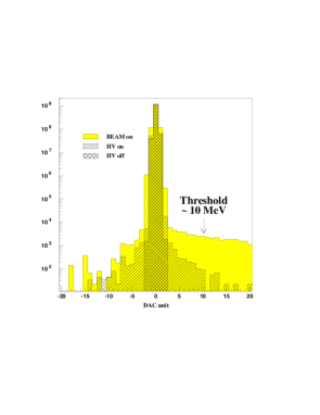
The noise and timing calibrations of the calorimetric ToF board will now be discussed. Fig. (5) shows, as function of the CFD threshold (in DAC units), the differential output CFD pulse rates measured by the TDC system (Sect. 6), with particles (beam on), without particles (HV on) and with photomultiplier high-voltages switched off. Each histogram sums up the 128 channels of the hadronic calorimeter. The narrower distribution, which measures the intrinsic electronic noise, is mainly contained within one bin and corresponds to a noise RMS of 67 V (0.3 MeV). This value, which is approximately 4 times the expected noise contribution from the preamplifier, indicates that the transmission of the high frequency range of SpaCal pulses is performed within a dynamic range of 15 bits. A similar value is obtained for the electromagnetic calorimeter, except for the channels of three analog boxes for which the RMS noise is increased up to 200 V, the extra noise contribution being induced by the low voltage power supplies. During data taking the CFD thresholds are set at a value of 20 MeV (10 MeV with the hadronic gain factor, see Fig. 5), well above the noise in order to ensure the long-term running stability.
The goal of the time calibration is to tune, channel by channel, the position of the ToF window. This is done by setting the switches of each channel in turn to the free position while all other channels are forced to null position, and then by delaying for two time settings of the electronic calibration pulses, the ToF window in steps of 1 DAC count of 270 ps, equal to the DAC step of the PDL (270 ps). The transition time of the AToF/ToF switching is recorded using the total energy trigger sums (Sect. 7) and is related to the corresponding TDC time of the electronic pulses (for a more accurate measurement of this transition time, the calibration system is pulsed five times for each step (see [19])). From the linear relationship between the TDC time and the PDL unit, the setting of the ToF window is calculated once the energy deposit time t corresponding to ep collisions has been measured. The start of the ToF window is set 2 ns earlier than t.
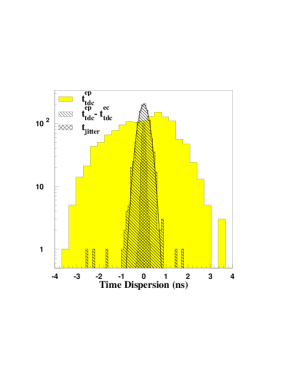
Fig. (5) shows for the 1192 channels of the electromagnetic calorimeter:
-
•
The dispersion of the raw t values as measured after one year of data-taking.
-
•
The relative time dispersion of t–t between t and the electronics calibration t. The narrow RMS width (0.23 ns) of the latter distribution as opposed to the 1.25 ns RMS width of the raw t one indicates that the dispersion of t is mainly generated between the calorimetric ToF board and the TDC system.
-
•
The dispersion of the transition time width from AToF to ToF (and the converse) as measured by the electronic pulses during the ToF window calibration. This distribution444For the display, the bin contents have been downscaled by a factor of .3, which is mostly included within one DAC unit (270 ps), indicates that the ToF window time jitter () has an RMS value lower than 0.08 ns.
Electronics tests have shown that the timing stability is better than 0.08 ns on the few minutes scale. On longer time scales there exist no means to perform this check since long term drifts of the trigger controller and beam interaction time with respect to the HERA clock are larger than 1 ns.
6 The TDC system
A system of about 1400 TDCs, one per photomultiplier, is needed to record the pulse timing in each SpaCal channel. This is necessary in order to be able to monitor and adjust the timing of the ToF/AToF switching in the trigger, as well as to distinguish offline between energy depositions coming from interactions rather than from beam-induced background.
Due to the first-level trigger latency, TDC results must be pipelined for at least 2.5s, but such TDCs are not available commercially. Therefore, a custom-made system has been built [20, 21], based on the commercially available TMC1004 [22, 23] (Time Memory Cell) developed for use on the Superconducting Super Collider.
Online monitoring was a serious consideration in the design. There is automatic on-board histogramming of the timing, for different types of trigger conditions, in order to allow checking of both the calorimeter and the electronics. There are also scalers for measuring the CFD output rates for calibration purposes as well as for on-line monitoring during data taking. The TMC chip and the way it is used in H1, the architecture and the boards of the TDC system, and the readout and on-line monitoring are described in the following subsections.
6.1 The TMC1004 ASIC
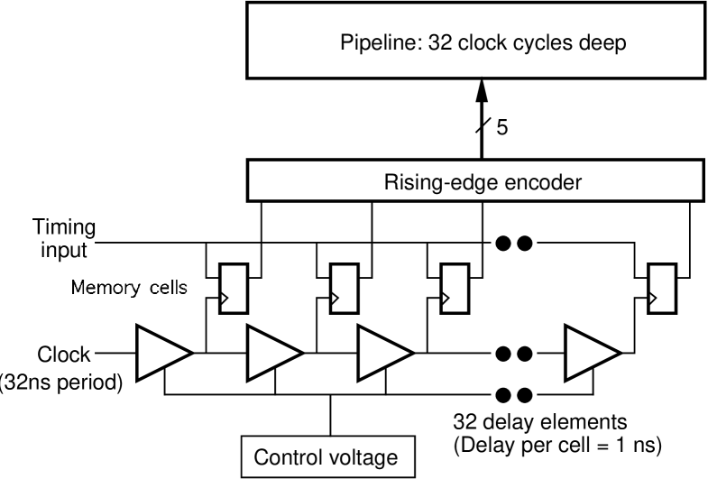
A conceptual diagram of the device is shown in Fig. 6. Each ASIC contains four channels, with individual timing inputs and a common clock. The digitisation is performed using a chain of 32 delay elements controlling the write inputs to a corresponding chain of memory cells. The timing input is connected to the data inputs of all the memory cells. A clock edge propagates down the chain of delay elements, storing the state of the timing inputs in the memory cells at intervals given by the delay of the delay elements. The position of a zero-to-one transition in the data stored in the memory cells indicates the time between the rising edge of the clock and the timing input signal. The data are stored in a pipeline, implemented as a circular buffer so its depth can be configured to be up to 32 clock cycles long.
The precision of the TMC1004 alone is specified to be 0.5 ns. The bin size, or accuracy of the TDC measurement, can be changed by varying the clock frequency, a feature available in the TDC system. The range over which the control of the delay is guaranteed is 0.6 ns to 1.5 ns, corresponding to clock frequencies of 50 MHz and 21 MHz respectively.
A TMC clock period of 32 ns, i.e. covering only one-third of a bunch crossing, is chosen. This is because the depth of the TMC1004 pipelines is only 1s if data are recorded continuously (32 32 ns), which is not long enough for the H1 trigger latency. The solution adopted, in order to avoid the need to extend the pipelines with external memories, is to record data from only one third of a HERA clock period per bunch crossing, which extends the length of the pipelines to 3s regardless of the TMC clock period. Experience showed that the full base-width of the ‘interesting’ part of the bunch crossing could be accommodated in the resulting 32 ns-wide active window. Thus, the normal situation for running uses a 31.3 MHz clock covering a window of 32 ns with a 1.0 ns bin size. However, the TMC clock multiple can be changed from its normal value of three to as much as five (52.1 MHz, covering 19.2 ns with a bin size of 0.75 ns) or to as little as one (10.4 MHz, covering the full 96 ns bunch crossing with a bin size of 3.0 ns). This trade-off means that precise measurements can be made over small windows, and cruder measurements can be made over the entire bunch crossing if necessary.
6.2 TDC system architecture
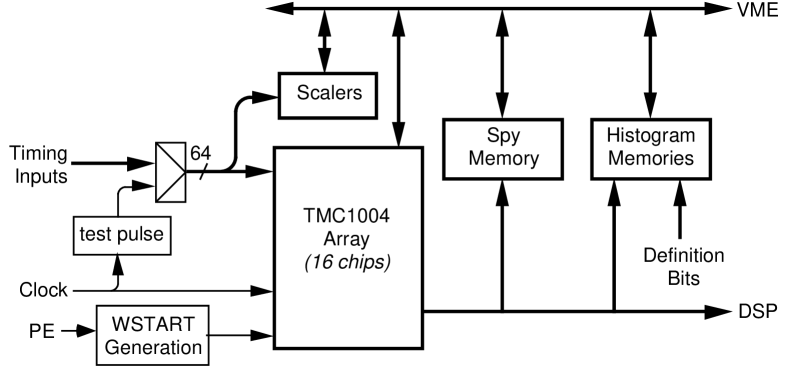
The TDC system is contained in two 9Umm deep crates with standard J1 VMEbus. The VMEbus is used for control and online monitoring, while readout to the H1 data acquisition system is via a dedicated bus to the same DSPs as the SpaCal energy read-out. A custom J2/3 bus using five-row DIN connectors allows for rear plug-in of all inputs, and the fanout of clock and control signals. The J2/3 bus also provides a separate acquisition bus over which data are sent to the readout DSPs. The TDC system is integrated into the SpaCal electronics as shown in Fig. 1.
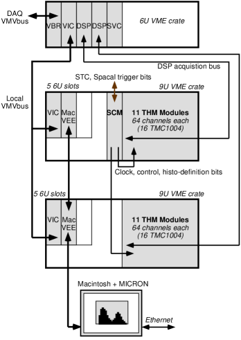
The TDC function is performed on 22 TDC and Histogrammer Modules (THMs, Fig.7), each with 64 channels and thus 16 TMC1004s. These modules receive the output CFD pulses from the front-end electronics via 23 m-long multi-way shielded twisted-pair cables. The THM includes also a 32-bit scaler per 16 TDC channels for the CFD rate measurements (Xilinx XC3020). Individual channels can be gated on or off, so that these scalers can be used either to monitor overall rates in blocks of 16 channels, or to examine individual channels one-by-one. The latter is useful not only in online monitoring, but also for setting the threshold of the front-end constant-fraction discriminators to be above the noise.
One System Controller Module (SCM) receives the central HERA bunch-crossing clock (10.4 MHz) and the Pipeline Enable (PE) sent by the L1 trigger. It multiplies the bunch-crossing clock by a programmable multiple, between one and five but normally three, to produce the TMC clock. The TMC clock and PE are fanned out to all THMs on equal-length cables. The SCM also provides 32-bit scalers for use by the monitoring software (e.g. number of bunch crossings, number of PEs, etc.). These are implemented in Xilinx XC3042s FPGAs.
The contents of the TDCs, scalers and histograms are accessible to a Macintosh-based C++ monitoring program. The use of a private bus for communication with the DSPs allows the Macintosh uninterrupted VME access, even during data-taking.
6.3 TDC read-out and monitoring
While the pipelines are enabled, the TMC chips acquire the time of arrival of energy with respect to the TMC clock for each channel. When a first-level trigger occurs (2.5s after the bunch crossing of interest) the pipelines are frozen, and data from the triggered bunch crossing as well as one either side for safety are accessible to calorimeter-readout DSPs. Two DSPs situated in a remote data-acquisition crate read the data over the local acquisition bus. Each DSP reads out one crate of THMs, zero-suppresses the data, and places them into a buffer for the event builder.
For online monitoring purposes, automatic histogramming of every channel using on-board memories was implemented. This allows the monitoring computer to read out filled histograms when it is convenient, rather than have to read out many events and build up the histograms itself.
There are actually 16 histograms per channel. Data from a given bunch crossing are added to the histogram specified by a set of four ‘definition bits’ fanned out from the SCM. The bits are generated from the SpaCal trigger bits using a RAM-based lookup table that allows specification of arbitrary logical combinations of trigger bits. In this way, the significance of the histograms is completely programmable and can be changed to allow different investigations to be carried out for different types of trigger in the SpaCal.
There is one histogrammer unit per 16 channels. Although only one of these channels can be selected for histogramming at a time, all 16 can be stepped through in sequence automatically. The histograms are stored in RAM, requiring 1024 32-bit words per channel. This gives a total of 5.5 Mbytes of histogram RAM in the TDC system. To histogram the data from a single bunch crossing takes eight bunch crossings, during which the histogrammer is insensitive. With zero-suppression this is acceptable, given the low occupancy of each channel.
These histograms, along with the scalers on the SCM and THMs, are accessible via VMEbus to the monitoring software for online checks and expert diagnoses.
7 Electron and Total Energy Triggers
7.1 Inclusive electron trigger
Since the current jet of a low Bjorken deep-inelastic event is boosted in the backward direction, a total energy sum cannot be used at the first level trigger to distinguish deep inelastic scattering events from photoproduction events (Q2 1 GeV2). We therefore apply a simple inclusive electron trigger condition that there is at least one trigger tower (44 SpaCal towers) energy greater than a threshold. More precisely, this inclusive electron trigger (IET) is designed to compare the deposited energy inside a group of 44 SpaCal towers with each of 3 thresholds. A global ‘OR’ of the digital outputs for each threshold is performed, the result of the three ‘OR’s being sent to the H1 first-level central trigger logic. The trigger tower size is chosen such as to ensure the transverse containment of the electromagnetic shower at any scattering angle .
The sliding trigger towers are formed as shown at the top of Fig. 9. From hardwired presums of the ToF-timed signals from 22 SpaCal towers (done in the calorimetric ToF card described in Sect. 5) the content of all presums (i.e. the overlaying sums of 16 SpaCal towers) is calculated (Fig. 9). In this way, even when the impact point is at the border of two presums (point B in Fig. 9), the full deposited energy is recovered in the trigger tower 3 (Fig. 9). As shown in this figure, the sliding summation is performed in both directions, x and y.
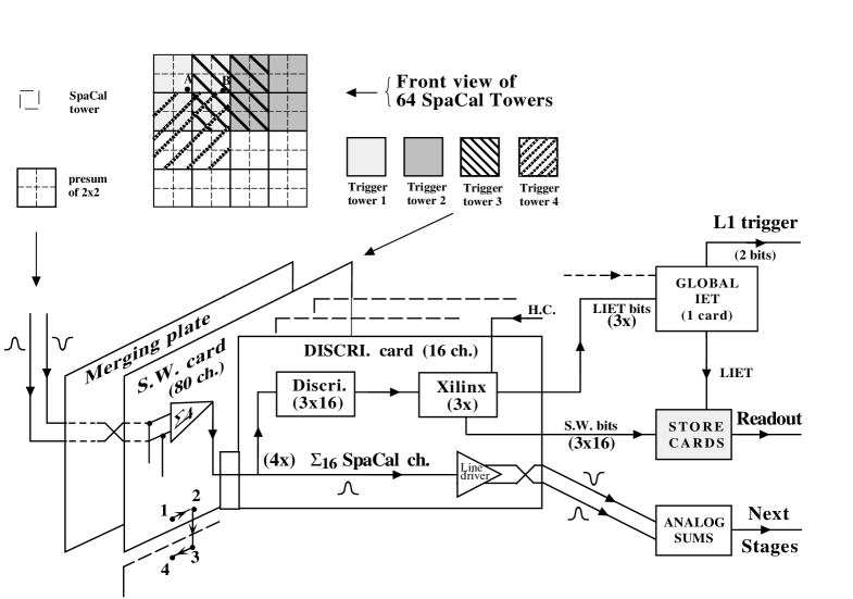
A schematic view of the electronics is shown in Fig. 9. The pulses (fixed presums) supplied by the calorimetric card are sent to the trigger electronics on shielded multi twisted-pair cables. The merging plate allows each presum to be individually mapped to the correct destination in order to do the sliding-sum calculation. As sketched in Fig. 9, a basic trigger crate consists of a Sliding Window (SW) card (80 channels) acting as a backplane, and Discriminator Cards (5) processing 16 channels each. The full trigger is contained in 5 such (3U 350 mm deep) crates. The main features of these two cards are:
-
Sliding Window Card: this is an 8-layer printed-circuit board, two layers used as voltage supply planes and the others for the distribution of the analog pulses. According to the sliding window scheme (Fig. 9), a differential presum pulse must be sent to 4 line-receivers and each line-receiver processes 4 presum pulses (acting then as summing amplifier). The receiver/summing amplifier (OPA620 from Burr-Brown) is the only active component of this card. Receiver outputs corresponding to trigger towers are gathered per group of 16 and sent to the discriminator card via a two-row DIN connector. The latter enables the fast signals to be fed with a minimal crosstalk of about 0.5 %.
-
Discriminator Card: The functions of this board are:
-
1.
To compare (AD790JR discriminators) the trigger tower pulse height with three thresholds.
-
2.
To supply, per threshold, a local ‘OR’ (named LIET bit for Local IET) of the 16 discriminated pulses. These are latched and synchronized with the HERA clock (HC) inside a Xilinx (XC 3020) which performs this ‘OR’. The individual bits (SW bits), corresponding to detailed trigger information used for debugging or analysis, are read out via ‘Store Cards’ ([24]).
-
3.
To pick-up the analog information of the 4 adjacent trigger towers and to drive them differentially to the summing electronics, as described below.
-
1.
As shown in Fig. 9, LIET bits are sent to a single card (named ‘global IET’). This board performs the ‘OR’ of the 25 LIET bits and supplies the encoded result to the central L1 trigger.
The main performance features of this trigger are as follows: the RMS output noise of a receiver/summing amplifier is equal typically to mV which is equivalent to 8 MeV. The cross-talk signal, generated inside the SW card, between trigger tower pulses, is of the order of , which is negligible. The amplitude dispersion at the output of the SW cards has been measured to be ([18]); no significant spatial pattern in the response of these cards was found, especially when the presums are distributed to two SW cards as indicated in Fig. 9.
7.2 Total energy trigger
In this section we describe the electronics (Fig. 10) used to generate the trigger elements of the total energy for both in time (ToF or ep) and out of time (AToF or background) events. They are based on the IET electronics and on two new boards, the Receiver card (80 channels) and the Summing card (16 channels) which can be arranged in a crate in a similar way as the SW and discriminator cards respectively. The receiver card is a simplified version of the SW card, the OPA620 being mounted in the usual line receiver configuration. The Summing card performs the analog sums or or input channels; the option of the sums is set inside the card by jumpers. This allows great flexibility for doing sums according to a given mapping.
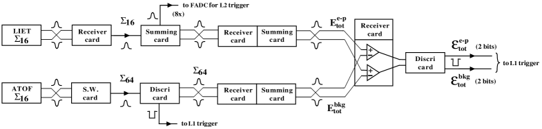
The 77 input channels of the summing electronics are processed differently for ep and background events, as can be seen in Fig. 10:
-
•
For ep events, the SpaCal channels with ToF signals supplied by the LIET cards are summed into 8 ‘big sums’ which correspond to large regions of the calorimeter (4 quarters of an inner square of 16 16 SpaCal towers and 4 quarters of the remaining outer shell). The 8 ‘big sums’ are fed into FADCs for the L2 trigger and, in parallel, to a final sum operation which provides the total energy E.
-
•
For events outside of the ToF window (AToF events), the SpaCal channels with AToF signals supplied by the calorimetric ToF cards are processed by an electron trigger crate (Fig. 10), using only one threshold for the energy comparison. The ‘OR’ of the 5 local AToF bits is sent to the L1 trigger. The purpose of the sliding sum board for AToF energies is to recover, at the output of the discriminator cards, the complete analog information for the total energy E summation. The latter is done in the same way as for the ep events (Fig. 10).
The right part of Fig. 10 shows that the quantities E–E and E–E are discriminated in place of the raw total energies Etot. This energy comparison is made to prevent spurious triggers which are attributable to the following :
-
1.
Inside the calorimetric ToF board, the slewing of the CFD outputs for small energy deposits ( CFD threshold value) can direct a non-negligible fraction of the total energy of the event towards the trigger branch with inappropriate timing (AToF instead of ToF or vice-versa).
-
2.
For an ep event, all energy deposits below the CFD threshold are not timed; they are sent by default to the AToF branch and can lead to a trigger veto.
-
3.
High frequency cross-talk inside the energy read-out and the ToF cards, summed over the 16 neighbouring channels.
The first two effects dominate at low energy and the last one at high energy (4% of AToF to ToF above 25 GeV and 2% ToF to AToF above 25 GeV).
As can been seen in Fig. 10, the subtraction is performed by feeding the same polarity of the two differential pulses into a line receiver amplifier of a Receiver card. The result of this analog subtraction is compared with two thresholds of a discriminator card.
Although H1 has not yet run with the SpaCal energy thresholds set to values below 600 MeV, the electronic noise alone allows 100 MeV thresholds for the IET, well below the 300 MeV level for a minimum ionising particle (mip).
8 Performance at HERA
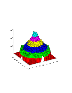
During normal running at HERA, the rate scalers (Sect. 6) are used in a mode where they cycle through all the SpaCal channels. Fig. 12 shows such a rate distribution; X and Y are the SpaCal tower numbers. This on-line histogramming, as well as the timing plots display of individual channels (not shown), have proven to be a valuable diagnostic of both the correct behaviour of the SpaCal and of the backgrounds due to the HERA beams. The rate distribution (Fig. 12) is peaked around the beam pipe at a value of about 15 kHz. This is due to the proton–gas collisions, physics events accounting for only a small fraction ( 10-3) of this distribution.
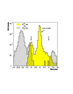
Studies of the performance of the SpaCal triggers can be achieved by recording events without the on-line rejection maintained by higher-level triggers during normal H1 data-taking. Fig. 12 shows a time distribution of events recorded during such a special run. The earlier peak is due to background energy deposits, while the second one corresponds to ep physics events, the small one in between coming from background due to the proton beam structure (proton satellite bunch).
In Fig. 12, the time of the event has been calculated off-line in the following steps:
-
1.
For the i-th cell, the raw time is corrected (t) from the offset t (sect.5) and the slew effect of the CFD,
-
2.
The event time is defined as the mean weighted time:
(7) where is the energy deposited in the -th cell. This linear weighting has the advantage of lowering the contribution of energy deposits which are approximately equal to the CFD threshold ( 40 MeV); for these low energies, the time is measured with a jitter of a few ns due to the noise fluctuation at the input of the CFD
-
3.
The ep distribution mean value is taken as the time origin. Due to the dispersion of the offsets , the effective histogramming time window is reduced from 32 ns to 25 ns. This window is still wide enough to contain both ToF events and proton beam background.
The two peaks of Fig. 12 are separated by 10 ns, as expected. The RMS width of the physics events peak is a direct measurement of the time resolution achieved by the SpaCal calorimeter and the electronics because the arrival-time dispersion of physics events in the calorimeter is negligible. A gaussian fit to data from events triggered by the total energy trigger (see Fig.10) with an energy threshold of MeV yields a time resolution value ns, dominated by TDC resolution. The width of the background peak is broader ( ns after subtraction of the 0.35 ns resolution) and is compatible with the proton bunch length measured, for instance, by the H1 central tracker detector ( ns). When including events triggered by lower energies, the resolution degrades from 0.35 ns at 600 MeV to 0.8 ns for 80 MeV (30 MeV) in the electromagnetic (hadronic) section.
As can be seen in Fig. 12, besides the two main peaks discussed above, there is a continuous time distribution of energy deposit. These events are related to background collisions of a proton satellite bunch with the residual gas. This satellite bunch is delayed with respect to the main proton bunch and varies in shape and intensity for different fills of the HERA machine.
These satellite background events can be used to study in-situ the transition AToFToF performed by the calorimetric ToF board. The shaded histogram includes events triggered by the total energy trigger with an energy threshold of MeV, while the hatched histogram corresponds to events which would have been rejected by the veto at the same threshold value (see Fig.10); due to the energy subtraction performed at the last electronics stage, no events are found simultaneously with the and trigger bits ON.
The spread of the events selected as “ep” events corresponds to the average ToF window width (10 ns) indicated by the vertical arrows. The transition AToFToF occurs within 0.5 ns RMS. The width of this transition region is compatible with the ToF window calibration error, dominated by the TDC resolution (and not by the slew time because these events are from high energy background). At energies around 1 GeV the transition would be broader due to slew effects.
The two overlap events located at 3 ns and 4.5 ns (Fig. 12) are easily identified from the off-line TDC information, as pile-up events of two consecutive bunches and are thus rejected.
As a conclusion about this on-line time-of-flight selection, it can be remarked that:
-
•
Events from the main proton peak are entirely rejected (about events). The remaining background due to the satellite bunches is of the order of of the main proton background. It can be reduced to the level of by an off-line timing analysis. A further factor 10 can be gained by using the hadronic section of the SpaCal [19].
-
•
For the 600 MeV cut on the total energy there is no loss of physics events. Below this energy threshold, the importance of event topologies requires a special treatment, as described in [19].
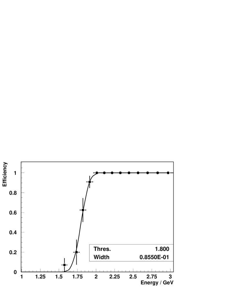
Fig. 13 shows the combined efficiency of the time-of-flight selection and the electron trigger IET, for one sliding sum. This curve is obtained from the H1 data according to the following procedure:
-
1.
Events triggered without a SpaCal energy requirement and with a reconstructed time in the interval of ns (Fig. 12) are selected,
-
2.
The deposited energy inside the trigger tower (Sect. 7.1) is calculated from the energy deposited in the SpaCal towers belonging to the trigger tower,
-
3.
Early or late pile-up events tagged by the 1 bunch-crossing TDC information are rejected.
During normal data taking, threshold values of the IET are set approximately to 0.5 GeV, 1.8 GeV and 5 GeV respectively. Fig. 13 shows that an efficiency of 100 is currently achieved above 2 GeV by the second threshold, used mainly to trigger deep inelastic scattering events; a similar performance has been shown (ref. [25]) for the lowest threshold where an efficiency of 100 % is reached at 600 MeV. The width of the threshold (Fig. 13) is found equal to 85 MeV. This value is 10 times greater than is expected from the total noise (8 MeV) of the analog sum (Sect.7.2). This discrepancy is due to the variation, from channel to channel, of the charge preamplification gain discussed in Sect. 3. According to the shaping performed in the next stages, this gain variation is more or less washed out; the longer shaping time of the readout branch implies that the shaped pulse amplitude is less sensitive to this gain variation than the one in the trigger branch. As the PM high voltages are tuned in order to balance the response of the channels in the readout branch, the reconstructed width of the trigger threshold is larger than what could be expected only from noise considerations. This gain effect leads to a threshold width proportional to the energy threshold, but is not a limitation for triggering with a high efficiency over the full energy range.
9 Summary
The electronics associated with the H1 SpaCal lead/scintillating-fibre calorimeters, in operation at HERA since 1995 has been described. The full electronics was specially developed to have the following functionality:
-
•
Wideband (200 MHz) low noise ( MeV) preamplification which uses the photomultiplier capacitance for charge integration. This preamplifier is, in principle, very general and can be applied to any low-capacitance detector.
-
•
For the readout branch, energy and time information for each cell is provided. In particular, the time information has proved to be very powerful for the off-line rejection of residual background or pile-up events. A time resolution of 0.8 ns is obtained for SpaCal total energies above 80 MeV (30 MeV) for the electromagnetic (hadronic) wheel.
-
•
For the trigger branch, the calorimeter time-of-flight is able to reject proton background events with a time resolution of 0.5 ns RMS. The low-noise electron trigger, based on analog sliding sums, running at the HERA frequency (10 MHz) enables the use of 100% efficient triggers with a cluster energy threshold as low as 0.5 GeV.
-
•
The low noise performance permits analog summation of the 1192 channels of the electromagnetic calorimeter. A minimum-bias total-energy trigger with a threshold of 0.6 GeV is currently used, yielding an out-of-time background rejection greater than 106 with no measurable overefficiency. This total-energy sum, together with the programmable switches of the calorimetric ToF board, are very powerful tools for the complete tuning and testing, channel by channel, of the electron and calorimetric triggers.
10 Acknowledgements
The members of the H1 SpaCal group extend their warm thanks to the H1 collaboration for its stimulating motivation and constant support, and acknowledge the outstanding commitment of the many engineers and technicians from the different institutes. The authors thank C. de La Taille for his invaluable help in the design of the preamplifier. The group also wishes to thank the DESY directorate for the hospitality extended to the non-DESY members.
References
- [1] H1 Collaboration, Technical Proposal to Upgrade the Backward Scattering Region of the H1 Detector, DESY PRC 93/02.
- [2] T. Nicholls et al., H1 SpaCal group, Nucl. Instr. and Meth. A374 (1996) 149.
- [3] R.D. Appuhn et al., H1 SpaCal group, Nucl. Inst. and Meth.A386 (1997) 397.
- [4] R.D. Appuhn et al., H1 SpaCal group, DESY 96-013.
- [5] E. Tzamariudaki, VII Int. Conf. on Calorimetry in HEP, Tucson, AZ, USA (1997).
- [6] J. Bán et al., Nucl. Instr. and Meth. A372 (1996) 399.
- [7] I. Gorelov, VI Int. Conf. on Calorimetry in HEP, Frascati, Rome, Italy (1996), Frascati Physics series vol.VI, pp 225-236.
- [8] S. Dagoret et al., Nucl. Instr. and Meth. A346 (1994) 137.
- [9] J. Janoth et al., Nucl. Instr. and Meth. A350 (1994) 221.
- [10] R.D. Appuhn et al., H1 SpaCal group, Nucl.Inst. and Meth. A404 (1998) 265.
- [11] V. Radeka, IEEE Trans. Nucl. Sci. NS 21 (1974) 51.
- [12] See e.g. C. de La Taille, Thèse de Doctorat (in French), Ecole Polytechnique, December 1989.
- [13] SECRE Composants, Paris, France.
- [14] R. Bernier et al., H1 internal note H1-07/92-237.
- [15] B. Andrieu et al., H1 Calorimeter group, Nucl. Instr. and Meth. A336 (1993) 460.
- [16] I. Abt et al., H1 Collaboration, DESY report H1-96-01 , DESY, Hamburg (1996) and Nucl. Instr. and Meth. A386 (1997) 310 and ibid. A386 (1997) 348.
- [17] R. Bernier et al., H1 internal note H1-04/92-219.
- [18] S. Spielmann, Thèse de Doctorat (in French), Ecole Polytechnique, July 1996.
- [19] P. Zini, Thèse de Doctorat (in French), Université de Paris VI, July 1998.
- [20] E. Eisenhandler et al., IEEE Trans. Nucl. Sci. 42 (1995) 688.
- [21] T. Nicholls, Ph.D. Thesis, The University of Birmingham, April 1997.
- [22] Y. Arai et al., IEEE Jour. of Solid State Circuits 27 (1992) 359.
- [23] Y. Arai et al., IEEE Trans. Nucl. Sci. 39 (1992) 784.
- [24] C. Beigbeider et al., H1 internal notes H1-10/92-242 and H1-02/93-269.
- [25] F. Moreau, V Int. Conf. on Advanced Technology and Particle Physics, Como (Italy) 1996, Nucl. Phys. B (Proc. Suppl.), 132. 61B (1998).