NOVEL RECONSTRUCTION MECHANISMS: A COMPARISON BETWEEN GROUP-III-NITRIDES AND ”TRADITIONAL” III-V-SEMICONDUCTORS
Abstract
We have studied the driving forces governing reconstructions on polar GaN surfaces employing first-principles total-energy calculations. Our results reveal properties not observed for other semiconductors, as for example a strong tendency to stabilize Ga-rich surfaces. This mechanism is shown to have important consequences on various surface properties: Novel and hitherto unexpected structures are stable, surfaces may become metallic although GaN is a wide-bandgap semiconductor, and the surface energy is significantly higher than for other semiconductors. We explain these features in terms of the small lattice constant of GaN and the unique bond strength of N2 molecules.
1 Introduction
Progress in the materials quality of GaN has led recently to the first commercially available, highly efficient optoelectronic devices emitting in the green and blue/UV region [1, 2]. A substantial problem in growing GaN and its alloys is the lack of a lattice-matched substrate. Bulk GaN can be grown only in small crystallites and sapphire, the most commonly used substrate, has an extremely large lattice mismatch (14%). Another problem is the high nitrogen vapor pressure of bulk GaN requiring highly activated nitrogen precursors for the growth. Both issues make it difficult to grow routinely and in a controlled fashion high quality GaN. In order to overcome these problems it is critical to understand the fundamental growth aspects on an atomic level.
Initially, it has been believed that the driving forces behind surface reconstructions and growth are essentially the same as for conventional semiconductors such as e.g. GaAs. However, it soon became obvious that GaN behaves in many aspects very differently. For example, impurity concentrations are significantly higher than in conventional semiconductors and p-type doping is rather difficult [3]. Also, growth is much more affected by even small changes in the growth environment and the structure of the initial nucleation layer at the substrate controls the properties and quality of the entire epitaxial layer.
Recent investigations also revealed surface structures for the technologically relevant polar GaN surfaces which are very different from the well-established structures of III-V semiconductor surfaces. Furthermore, some of these structures disobey well-accepted empirical rules and models, which have been found useful for understanding why and how semiconductor surfaces reconstruct. For example, on cubic GaN (001) (which is commonly used to grow the cubic phase of GaN) first-principles calculations identified a Ga-terminated surface as the energetically most stable structure. On this surface four Ga atoms form linear tetramers [4]. This is in contrast to conventional semiconductors where dimers are the preferred building blocks on (001) surfaces. Another example is the Ga adlayer structure which has been found combining detailed STM and LEED measurements with first-principles calculations at the wurtzite GaN surface [5]. This surface violates several rules: It disobeys electron counting, atoms in the top surface layer sit on singly coordinated sites, and each surface atom has the highest possible number of dangling-bond states.
The aim of the present paper is to identify the properties of GaN that give rise to these unusual surface reconstructions, to understand why the empirical rules that have been well established to describe conventional semiconductor surfaces fail for GaN, and to determine whether these rules can be extended to GaN. We will focus here on the mechanisms and general principles of the surface reconstructions. Detailed descriptions of the specific atomic structures and the calculations for cubic and wurtzite GaN can be found in Refs. [4, 5]. After a brief description of the computational details (Sec. II) we will analyze the surface energies of unreconstructed GaN and GaAs surfaces. Based on these results we show that a characteristic feature of GaN surfaces is the tendency to have Ga atoms in the surface layer. This feature, combined with the small lattice constant, is shown to be responsible for the unusual surface reconstructions. Finally, based on this analysis we derive conclusions concerning possible surface reconstructions.
2 Computational method
The energy necessary to create a surface is called the surface energy. This energy is not constant but depends on the specific thermodynamic conditions. Specifically, in GaN the relative concentration of Ga and N atoms at the surface determines the surface energy. The atomic reservoirs with which Ga and N atoms are exchanged in order to modify the surface stoichiometry determines the chemical potentials (, ). The chemical potentials for Ga and N are not independent variables, since for thermal equilibrium situations both species are in equilibrium with the GaN bulk:
| (1) |
The surface energy at and is then given by:
| (2) |
where and are the number of Ga and N atoms and is the total energy of the surface obtained from density-functional theory.
The gallium chemical potential can be varied only between certain limits. A major criterion is that the chemical potential for an element is less than the chemical potential of the corresponding bulk material (or molecules) since otherwise this element would form the energetically more stable bulk or molecular structure. For the gallium chemical potential an upper limit is therefore given if GaN is in thermodynamic equilibrium with bulk Ga. This case is called the Ga-rich limit. The lower limit is given for GaN in thermodynamic equilibrium with N2 molecules; it is therefore called the N-rich limit. Using these relations and Eq. (1) we get:
| (3) |
Here, is the heat of formation which is defined as:
| (4) |
A negative heat of formation means the reaction is exothermic. The corresponding bulk chemical potentials are calculated from the bulk forms of Ga metal (orthorhombic), N (N2 molecule) and GaN (wurtzite). The total energies have been calculated employing density-functional theory in the local density approximation, in combination with a plane-wave basis set and first-principles pseudopotentials. The exchange and correlation energy functionals are those derived from the homogeneous electron gas calculations of Ceperley and Alder [7]. We use soft Troullier-Martins [8] pseudopotentials constructed with the fhi98PP package [9]. An explicit treatment of the Ga electrons as valence electrons has been found crucial to calculate accurate surface energies. This required a large plane wave energy cutoff making our calculations computationally rather challenging both with respect to CPU-time and memory demand. We therefore used a parallel version of our plane wave code on a Cray T3E. This version had been specifically optimized with respect to data and CPU partitioning. Details about the program can be obtained from Ref. [10].
3 Analysis of the surface structures
As pointed out in Sec. 1, surface reconstructions of GaN exhibit features that have not been observed on other III-V semiconductor surfaces. In order to identify the mechanisms causing the unusual reconstruction we will analyze the differences between polar GaN and GaAs surfaces. We will focus on polar surfaces since non-polar surfaces show essentially the same features as found for conventional semiconductors [14]. Since we are here interested in the mechanisms driving surface reconstructions on GaN surfaces let us first briefly recall the rules and models that are typically applied in a discussion of conventional semiconductor surfaces. A commonly used principle is called the electron counting rule (ECR). According to the ECR the equilibrium surface is one in which the number of available electrons in the surface layer will exactly fill all dangling-bond states in or near the valence band and leave all states in or close to the conduction band empty [11]. An important consequence of this rule is that a surface satisfying the ECR will be semiconducting. Further, just by counting electrons and dangling-bonds a large number of potential surface structures can be eliminated. While this rule is empirical, it has been found to work well for almost all conventional semiconductor surfaces. Only a few exceptions have been reported [16, 20].
The ECR is commonly justified in terms of Harrison’s bond-orbital model [12]. Atoms in conventional semiconductors are sp3 hybridized. In the absence of reconstruction some of the hybrid orbitals cannot form bonds, but instead give rise to partially occupied sp3 dangling-bond states. According to Harrison the energy levels of the cation dangling-bond states are high in energy (lying close to or within the conduction band) and should therefore be empty. Dangling bond states localized on the more electronegative anions, however, are close to or within the valence band and should be filled. Other mechanisms driving the reconstruction at semiconductor surfaces are: (i) the tendency to reduce the number of dangling bond states on the surface by forming e.g. dimers, adatoms or trimers [20, 21] and (ii) minimizing the electrostatic energy by optimizing the arrangement of charged surface atoms [13].
3.1 Reconstruction mechanisms for ”traditional” semiconductors
We will start our comparison between GaAs and GaN by considering the simplest possible surface structures - the unreconstructed (1x1) surfaces. These surfaces (Fig. 1) are terminated either by cations or by anions. For GaAs possible structures are the open (001) surface and the close-packed (111) (cation-face) and () (anion-face) surfaces. Since the equilibrium phase of bulk GaN is the wurtzite structure we performed the calculations for (0001) (cation-face) and () (anion-face) which are equivalent up to the fourth nearest neighbors to the cubic (111) and () surfaces. Since we are here only interested in qualitative aspects, we will consider the (111)/() and (0001)/(000) as equivalent surfaces.
3.2 Comparison between unreconstructed GaAs and GaN surfaces
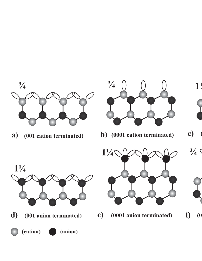
The calculated surface energies of GaAs are plotted as a function of the chemical potential in Fig. 2 (a-c). The energies are fully consistent with the empirical rules and models discussed above. First, both Ga and As-terminated (1x1) surfaces have much higher surface energies than the reconstructed equilibrium surfaces implying that the (1x1) surfaces are unstable against surface reconstruction. This is consistent with the fact that all possible polar (1x1) surfaces have partially occupied dangling bonds and thus disobey electron counting. Further, consistent with the principle of reducing the dangling bond density, both the Ga-terminated (111) and the As-terminated () surfaces that have only one dangling bond orbital per surface atom (see Fig. 1b and 1c) are energetically more stable than the corresponding As and Ga-terminated surfaces that have three dangling-bond orbitals per surface atom.
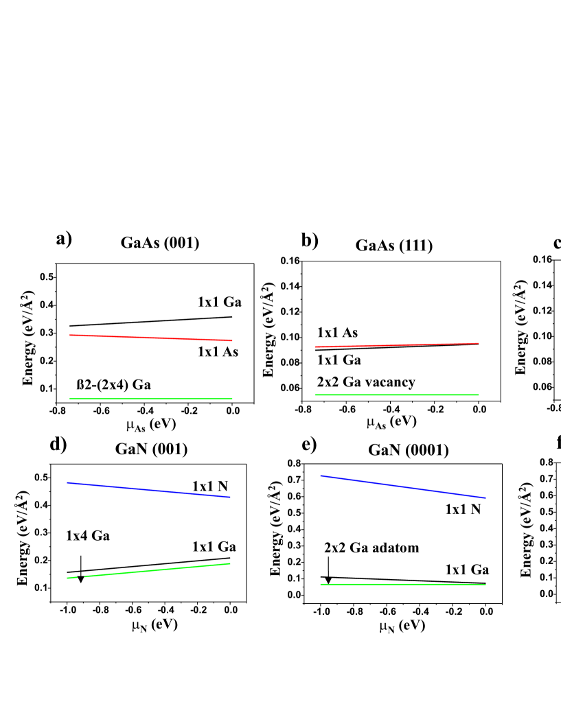
For GaN (Fig. 2, d-f) some of these mechanisms are no longer valid. First, N-terminated surfaces are energetically always less stable than the corresponding Ga-terminated surfaces. This result applies even for the (000) surface where the Ga-terminated surface has three (Fig. 1f) and the N-terminated surface only one dangling bond orbital per surface atom (Fig. 1c). Second, the Ga-terminated surfaces have a very low surface energy, which is only slightly higher than the surface energy of the reconstructed equilibrium surfaces. This is in clear contrast to GaAs where all unreconstructed surfaces are much higher in energy than the equilibrium structures. In fact, for (000) the Ga-terminated (1x1) structure (Fig. 1f) becomes the energetically preferred structure under Ga-rich conditions (see Fig. 2f). This structure, however, obviously disobeys the electron counting rule.
3.3 Reconstruction mechanisms on GaN surfaces
From these results we can immediately conclude that a major mechanism driving GaN surface reconstructions is the tendency to stabilize structures that have more Ga than N atoms in the surface layer. This conclusion is also consistent with recent experimental and theoretical studies on GaN surface reconstructions [5]. Almost all equilibrium surfaces consist solely of Ga atoms in the top surface layer. The only exception for polar surfaces is the (0001) surface, where under nitrogen-rich conditions N-adatoms can be stabilized on a Ga-terminated surface [5, 26]. This feature of preferring just one species in the top surface layer (independent on the chemical potentials) is unique to GaN and has not been reported for other semiconductor surfaces. We will therefore attempt to elucidate the mechanisms responsible for the stabilization of Ga atoms in the surface layer. According to Eq. (2) we can seperate the surface energy into two contributions: (i) the energy necessary to remove or add atoms to the chemical reservoirs (which describe the specific growth conditions) and (ii) the total energy which is the sum over all bond energies and includes contributions such as charge transfer, electrostatic energy etc.
3.4 Chemical Potentials
Let us first focus on the chemical potentials. A lower limit on the energy necessary to remove atoms from a chemical reservoir is the bulk cohesive energy for solids and the binding energy per atom for molecules. These energies are shown in Tab. 1 (taken from Ref. [15] for a selected number of elements). The elements have been chosen to be the constituent species of the major semiconductor materials. Let us exclude for a moment group IV elements which will be discussed at the end of Sec. 4.1. Among group II, III, V, and VI elements nitrogen is obviously the element with the highest binding or cohesive energy: The N-N bond in the N2 molecule is one of the strongest bonds found in nature. All other atoms have energies roughly between 2 - 3 eV, i.e. more than 2 eV less than a N atom in the N2 molecule. We can therefore conclude that for all compound semiconductors (except for group III-Nitrides) there are only modest differences in the chemical potentials. For group III-nitrides, however, there is a strong asymmetry in the chemical potentials: More energy is required to transfer N atoms from the N reservoir to the surface than to transfer Ga atoms to the surface.
| Element | Zn | Al | Ga | In | N | P | As | O | S | Se |
|---|---|---|---|---|---|---|---|---|---|---|
| Ecoh (eV) | 1.35 | 3.42 | 2.81 | 2.52 | 4.91 | 3.28 | 2.96 | 2.58 | 2.87 | 2.35 |
A rough estimate of how this asymmetry affects the energy of the GaN surfaces can be obtained by artificially eliminating the large difference in the chemical reservoirs for Ga and N. We therefore shift the Ga-chemical potential by the difference between the N and Ga chemical potential (2.1 eV). The energy to remove a Ga atom is then the same as removing a N atom from its chemical reservoir. The corresponding surface energy is shown in Fig. 3 as dashed line. The energy significantly increases (by ) bringing the surface energy closer to that of GaAs.
3.5 Metallic bonding
The fact, that gives only 2/3 of the difference with respect to the GaAs surface energy (Fig. 3) indicates that the difference in chemical potentials is not sufficient to explain the unusual stability of the Ga-terminated surfaces at GaN. It is also determined by the binding energy an atom gains if it is incorporated in the surface. The different binding energies on both surfaces can be mainly understood by the formation of second nearest neighbor bonds between surface Ga atoms. This effect can be roughly estimated by calculating the formation energy of a free-standing Ga layer at different lattice constants. The resulting energies shown in Fig. 4 reveal two interesting aspects: First, the equilibrium lattice constant of the free-standing Ga layer is close to the lattice constant of GaN bulk. Therefore, the energy the Ga-layer gains when relaxing from the GaN-bulk lattice constant to its ideal value is modest (0.2 eV). This feature implies that at GaN surfaces the Ga atoms can form metallic bonds similar to those in bulk Ga even without any relaxation. Second, by going from the GaAs bulk lattice constant to the GaN lattice constant the binding energy of the free-standing Ga layer significantly decreases (by 0.9 eV). This energy gain explains largely the stronger bonding energy ( in Fig. 3) of Ga atoms on the GaN surface. The energy reduction obtained by contracting the lattice constant of a Ga adlayer from the GaN-bulk value to the equilibrium value has been invoked to explain the stability of a laterally contracted incommensurate Ga-adlayer structure on the GaN(0001) surface[23].
3.6 Chemical trends
The above discussion explains the preference for having exclusively one species in the surface layer and the tendency to stabilize structures with low-coordinated configurations that are not observed for conventional III/V semiconductor surfaces. For these materials, the surface atoms prefer three-fold coordinated configurations (i.e. surface atoms have a maximum of one dangling bond) and the dominant surface species changes when going from cation to anion-rich conditions. Based on the cohesive energies shown in Tab. 1, we expect similar features (preference of one species, low-coordinated sites) for the other group III-nitrides (InN, AlN) and also for SiC.
4 Surface reconstructions on GaN surfaces
The arguments given above are general and apply to any polar GaN surface, because specific differences between the various surface orientations were not used. However, as can be seen in Fig. 1 the local configuration and the number of nearest neighbor bonds at the surface atoms depend strongly on the surface orientation: for the (001) surface the atoms are two-fold coordinated while for the (111) and () surfaces they form one or three bonds. We will therefore elucidate in the following how these specific arrangements affect surface reconstructions and compare with reconstructions found on GaAs.
4.1 The cubic GaN (001) surface
We will start with the cubic (001) surface. For GaAs, a detailed analysis of STM measurements by Pashley [11] revealed a set of rules which determine the reconstructions of equilibrium surfaces: Surfaces form (2x) reconstructions where the 2x periodicity arises from the formation of dimers and the periodicity arises from the missing surface dimers. These rules combined with the electron counting rule largely restrict the number of possible surface structures. Northrup and Froyen added later the principle of minimizing the electrostatic energy and identified the (2x4)-2 surface (which obeys all the rules) to have the lowest energy under moderately As-rich conditions [13].
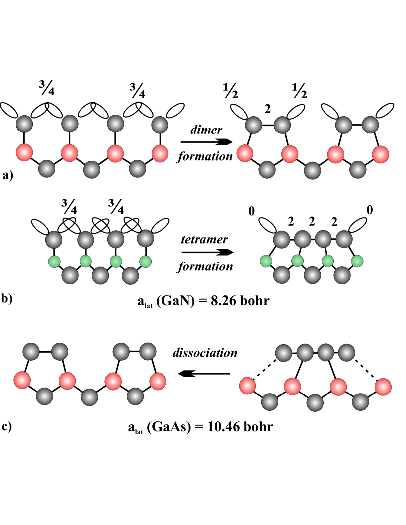
In general, dimers are considered to be the natural building block of surface reconstructions on (001) surfaces and have been observed also for other materials (e.g. AlAs, Si, SiC). The formation of surface dimers is energetically favorable since it reduces the number of dangling bond states by a factor of two. More important, due to the specific arrangement of the atoms on the (001) surface dimers can be formed simply by rotating the back bonds of the surface atom without stretching them (see Fig. 5a). While it is apparent that the formation of dimers is energetically preferred over the unreconstructed surface, it is by no means obvious why other building blocks than dimers should not be formed. Looking at the driving forces for dimers these alternative ’building blocks’ should further reduce the number of dangling bonds without significantly stretching the back bonds of the surface atoms. The simplest way to do this is to form ’-mers’ instead of dimers where surface atoms form a linear chain (an example for = 4 is shown in Fig. 5b). The number of dangling bonds is then reduced by a factor of 2/2 = where 2 is the number of dangling bond states at the unreconstructed surface and 2 the number of dangling bond states per “-mer”. For a dimer we obtain thus a factor of 2 while for a tetramer as shown in Fig. 5b a factor of 4 is achieved: Using these building blocks the number of dangling bonds at surfaces can be much more efficiently reduced than by forming dimers. The tetramer structure as shown in Fig. 5b has also another remarkable feature. It obeys electron counting (each of the three bonds in the tetramer holds 2 electrons and the two remaining dangling bonds are empty/filled if the tetramer consists of cations/anions). Thus, in contrast to the dimer structures, which require a combination of dimers and missing dimers in the surface unit cell, a (1x4) unit cell with a single tetramer is already sufficient to fulfil the ECR.
We have therefore performed calculations for a Ga tetramer on GaAs and GaN. For GaAs we find that a tetramer structure is unstable: without any barrier it spontaneously dissociates into two dimers. The reason for the instability becomes obvious when looking at the geometry as shown in Fig. 5c. In order to form the Ga-Ga bonds in the tetramer the back bonds of the outer atoms (marked by dashed lines) have to be stretched by more than 20% implying that these bonds are virtually broken. For GaAs, the elastic energy necessary to create the tetramer is larger than the energy gained by reducing the dangling bond density. For GaN, however, our calculations reveal Ga tetramers to be lower in energy than a structure consisting of two dimers. In fact, detailed calculations for a large set of possible surface geometries (including those stable on GaAs surfaces) revealed that the tetramer structure is actually the energetically preferred structure [4]. From Fig. 5b we see that the Ga-Ga bonds in the tetramer can be formed almost without stretching the back bonds of the outer atoms: The length of the back bonds increases only by 5% compared to the unreconstructed surface. The reason is simply given in terms of geometric ratios. Since the Ga-Ga bond length remains largely independent of whether the bonds are formed on GaAs or GaN, the stretching of the back bonds and thus the elastic energy becomes smaller with decreasing lattice constant (see also Fig. 5b). This explains why tetramers are stable on GaN ( bohr) but not on GaAs ( bohr). Based on these arguments we expect very similar structures for the other group III-nitrides (AlN, InN).
4.2 The closed packed (0001) and (000) GaN sufaces
We will now focus on reconstructions on the close-packed cubic (111) and () structures which are equivalent up to 4th nearest neighbors with the wurtzite (0001) and (000) surfaces. A main difference of these surfaces with respect to the (001) surface discussed above is the hexagonal symmetry () and the lack of a preferred axis along which dimers can be formed. Consequently, the formation of dimers always destroys the point group symmetry of the surface. In fact, dimer geometries have never been reported for these surface orientations. Experimental and theoretical studies showed that surface structures are commonly characterized by the formation of adatom, trimer and vacancy structures [20]. These structures are usually formed in a (2x2) surface unit cell and can be shown to obey electron counting [21].
Let us now consider the GaN (0001) surface. As has been pointed out in Sec. 3 the energetically preferred (1x1) structure is the Ga-terminated surface with one dangling bond state per surface atom (Fig. 1c). This structure is compatible with the principles of having mainly Ga-atoms in the surface and a low dangling bond density. However, first principles calculations showed that this structure is not stable: (2x2) adatom structures that satisfy the electron counting rule are lower in energy [5, 26]. These results are also consistent with recent STM investigations, where mixtures of Ga and N adatoms on these surfaces and semi-insulating behavior have been found [22].
For GaN (000) the tendency to prefer Ga atoms in the surface layer prevails over all other principles. A Ga-terminated (1x1) structure becomes energetically most stable despite having a maximum number of dangling bonds (three per surface atom) and clearly disobeys electron counting (Fig. 1f). Similarly, on the AlN (000) surface a (1x1) Al-adlayer becomes stable under Al-rich conditions [24].
5 Conclusions
Based on first-principles calculations we have studied the driving forces governing surface reconstructions on GaN. The principal mechanisms are (i) the tendency to stabilize Ga atoms in the surface layer, (ii) to obey electron counting and (iii) to reduce the number of dangling bonds. While (ii) and (iii) are well-known mechanisms driving surface reconstructions on other semiconductor materials (i) is a unique property of GaN, and more generally of all group-III-nitrides. The strong tendency to stabilize Ga-rich surfaces is not only a new property without any analogue among other compound semiconductors but it also prevails over the other principles. The most extreme example is the (1x1) Ga-adlayer structure shown in Fig. 1f. This is a metallic structure [5, 23] in which the number of dangling bonds is maximized.
These rules are of course too simplistic to derive a priori, i.e. without input from experiment or without performing realistic calculations. However, despite their simplicity these rules have been very successful in explaining or identifying surface reconstructions for a wide range of semiconductors. The knowledge of these mechanisms is not only important to derive conclusions concerning surface reconstructions but also about other properties of the surface. For example, an immediate consequence of the fact that polar GaN surfaces consists mainly of Ga atoms is a decreasing surface energy when going from N-rich to Ga-rich conditions (see Eq. (2)). This might explain why the surface morphology of GaN appears to improve when growing under more Ga-rich conditions [18, 19]. It also explains the exceptionally low diffusion barriers of Ga adatoms on these surfaces (0.2 - 0.6 eV) compared to barriers of 1.5 eV on GaAs [19]: Since the surface layer is comprised mainly of Ga atoms, the Ga adatom forms primarily Ga-Ga bonds which are weak compared to the Ga-N bond (metallic Ga melts already at room temperature). In breaking these bonds to jump from one adsorption site to the next, the Ga adatom must therefore overcome only a small energy barrier [25].
As has been pointed out in detail in Sec. 3 the origin of the stability of Ga-rich surfaces is (i) the large difference in the energies of the chemical reservoirs and (ii) a significantly smaller lattice constant compared to conventional III/V compound semiconductors. We expect therefore a very similar behavior for the other group III-nitrides, i.e. AlN and InN and their alloys.
6 Acknowledgements
We gratefully acknowledge financial support from the BMBF, the ”Fond der Chemischen Industrie” (T.Z.), and the ”Deutsche Forschungsgemeinschaft” (J.N.).
References
- [1] S. Nakamura, T. Mukai, and M. Senoh, Appl. Phys. Lett. 64, 1687 (1994).
- [2] S. Nakamura et al., Appl. Phys. Lett. 70, 868 (1997).
- [3] F. A. Ponce, D. P. Bour, Nature 386, 351 (1997).
- [4] J. Neugebauer, T. K. Zywietz, M. Scheffler, J. E. Northrup, C. G. Van de Walle, Phys. Rev. Lett. 80, 3097 (1998).
- [5] A. R. Smith et al., Phys. Rev. Lett. 79, 3934 (1997).
- [6] A. Kley, Dissertation, TU Berlin 1997.
- [7] D. M. Ceperley, B. J. Alder, Phys. Rev. Lett. 45, 567 (1980).
- [8] N. Troullier, J. L. Martins, Phys. Rev. B 43, 1993 (1991).
- [9] M. Fuchs, M. Scheffler, Comput. Phys. Com., submitted. http://www.fhi-berlin.mpg.de/th/fhi98pp/.
- [10] M. Bockstedte, A. Kley, J. Neugebauer, M. Scheffler, Comput. Phys. Com. 10 7, 187 (1997). http://www.fhi-berlin.mpg.de/th/fhi96md/.
- [11] M. D. Pashley, Phys. Rev. B 40, 10481 (1989).
- [12] W. A. Harrison, J. Vac. Sci. Technol. 16, 1492 (1974).
- [13] J. E. Northrup and S. Froyen, Phys. Rev. B 50, 2015 (1994).
- [14] J. E. Northrup and J. Neugebauer, Phys. Rev. B 53, 10477 (1996).
- [15] Handbook of Chemistry and Physics, Ed. D. R. Lide, 76, (1996).
- [16] L. J. Whitman, P. M. Thibado, S. C. Erwin, B. R. Bennett, and B. V. Shanabrook, Phys. Rev. Lett. 79, 693 (1997).
- [17] H. Yang et al., Appl. Phys. Lett. 68, 244 (1996).
- [18] D. Schikora, M. Hankeln, D. J. As, K. Lischka, Phys. Rev. B 54, R8381 (1996).
- [19] A. Kley, P. Ruggerone, M. Scheffler, Phys. Rev. Lett. 79, 5278 (1997).
- [20] D.K. Biegelsen, R.D. Bringans, J.E. Northrup, and L.-E. Swartz, Phys. Rev. Lett. 65, 452 (1990).
- [21] E. Kaxiras, K. C. Pandey, Y. Bar-Yam, J. D. Joannopoulos, Phys. Rev. Lett. 56, 2819 (1986).
- [22] A. R. Smith, R. M. Feenstra, D. W. Greve, M. S. Shin, M. Skowronski, J. Neugebauer, J. E. Northrup, submitted to Surface Science
- [23] A. R. Smith, R. M. Feenstra, D. W. Greve, M. S. Shin, M. Skowronski, J. Neugebauer, J. E. Northrup, J. Vac. Sci. Technol. B 16, 2242 (1998).
- [24] J.E. Northrup, R. Di Felice, and J. Neugebauer, Phys. Rev. B 55, 13878 (1997).
- [25] T. K. Zywietz, J. Neugebauer, M. Scheffler, Appl. Phys. Lett. 73, 487 (1998).
- [26] K. Rapcewicz and M. B. Nardelli and J. Bernholc, Phys. Rev. B 56, R12753 (1997).