The ATLAS pixel detector
Abstract
After a ten years planning and construction phase, the ATLAS pixel detector is nearing its completion and is scheduled to be integrated into the ATLAS detector to take data with the first LHC collisions in 2007. An overview of the construction is presented with particular emphasis on some of the major and most recent problems encountered and solved.
keywords:
vertex detector, pixel detector, radiation damage1 Introduction
The LHC proton-proton collider is expected to operate at a center-of-mass energy of , a bunch-crossing rate of and a design luminosity of . With the data recorded by the multi-purpose detectors, ATLAS and CMS, the mechanism of electroweak symmetry breaking and physics beyond the Standard Model will be explored. The high radiation environment and the large data rate pose severe constraints on the detector technology, in particular for the inner detectors. In ATLAS, the inner detector consists of a pixel inner tracking subsystem, surrounded by a silicon microstrip and a transition radiation trackers. The lifetime equivalent neutron dose which need to be sustained by the pixel detector is or neutron equivalent.
2 Overview
The pixel detector TDR98 is arranged in a cylindrical symmetry around the beam pipe (barrel) and in addition two end-cap subsystems (plugs) in the forward and backward region. The three barrel layers are located at a distance of , and from the beam axis and are equipped with 1456 partially overlapping identical pixel modules. Each endcap consists of three parallel planes at a nominal distance of , and from the interaction point and houses 288 modules. This geometrical arrangement allows a coverage in pseudorapidity for tracks with .
3 Modules
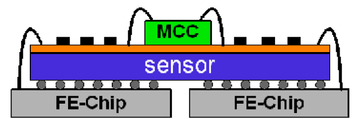
The basic unit of the pixel detector is a module. It consists of a silicon sensor, 16 front-end read-out chips arranged in two rows of 8 chips, a Kapton flex circuit with the Module Controller Chip and a pigtail connector. A schematic cross section view of a pixel module is shown in Fig. 1.
The sensor sensor has an active area of . The 47268 pixels are implemented as implants on the read-out side in thick oxygenated float-zone silicon n-bulk material. Radiation damage will type invert the sensor bulk and then increase the depletion voltage. A multiple guard-ring structure on the back side of the sensor allows for a maximum bias voltage of . This will provide nearly full depletion even after ten years operation in the LHC environment.
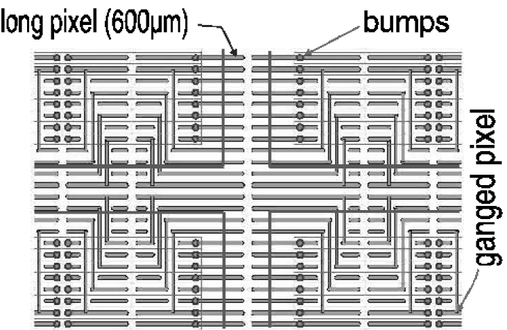
Each pixel cell has the dimensions which will provide a point resolution of in the coordinate testbeam . In the regions between front-end chips, pixels have either a modified geometry ( ) or are connected with each other, such that, at the cost of ambiguous reconstruction of hit positions, there is no dead area on the sensor surface (Fig. 2).
The silicon sensor is connected to the read-out front-end chips through fine pitch bump bonding with the flip-chip technique to form a bare module. The bump bonds provide electrical, mechanical and thermal contact at the same time. This fabrication step was done by two different providers, IZM and AMS, with PbSn and In technology, respectively.
The front-end chip FE-I3 is described in detail elsewhere Ivan . It is implemented in a standard CMOS process with a radiation tolerant layout, which has been demonstrated up to of total dose. It contains 2880 read-out cells, arranged in a matrix matching the sensor pixel geometry. In the analog section the charge deposited in the sensor is amplified and compared to an individually tunable threshold by a discriminator. The digital readout buffers the pixel address, a time stamp, and the signal amplitude as time-over-threshold (ToT) of hits. Hits which are selected by trigger signals within the Level 1 latency () are read-out, otherwise they are deleted.
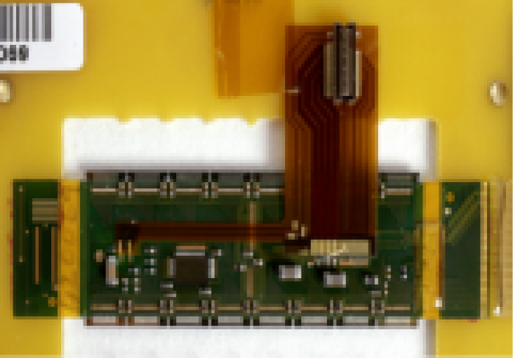
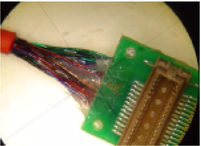
The last step of module assembly (“dressed module”) consists in gluing a flexible Kapton (flex) printed-circuit board to the back side of the bare module and connecting it through ultrasonic micro-wirebonds (Fig. 3). The flex contains passive components and the Module Controller Chip (MCC) MCC which steers the communication between the data acquisition system and the front-end chips. Event building and error handling are managed at this stage by the MCC.
All module components have been extensively tested in irradiation runs to ensure that the operation of the pixel detector will be possible even after the expected lifetime dose of . Seven fully assembled production modules were irradiated and tested in the laboratory. A typical noise increase of only 10% was observed. Other modules were characterized in a test beam, showing an almost fully depleted sensor, slightly reduced charge collection efficiency due to trapping, and excellent performance in high rate tests. See ref. testbeam for details.
4 Production and integration
Approximately front-end chips have been produced on 250 wafers with a yield exceeding . Extensive testing was performed on each wafer before and after bumping, thinning down to and dicing. At the bare module level, the front-end chips were again tested, in particular to detect defective bump bonds. A reworking procedure has been developed to recover these modules with high efficiency. Approximately 10% needed to undergo reworking. The recovery efficiency was 90%, averaged over the two vendors.
Approximately 2000 modules have been assembled and tested at five production sites (Fig. 3). Each module receives a ranking penalty measured in equivalent dead channels (edc) which determines the later placement of the module in the detector. Only 4% of the modules were rejected at this stage.
Laboratory measurements on production modules are described in detail elsewhere Jorn . For the threshold scan different charges are artificially injected and the number of hits recorded. Thus the threshold of the discriminator can be determined and adjusted for each individual channel. The timewalk is measured to ensure that hits can be associated to the correct bunch crossing during normal data taking at LHC. The module is then illuminated with a radioactive source to determine dead or inefficient pixels. The ToT response is calibrated into charge using the on-chip injection circuit and verified to agree to expectations based on the radioactive source measurement.

Figure 4 shows a distribution of dead channels for the modules chosen for the innermost layer. More than 300 modules resulted with less than 10 dead channels.
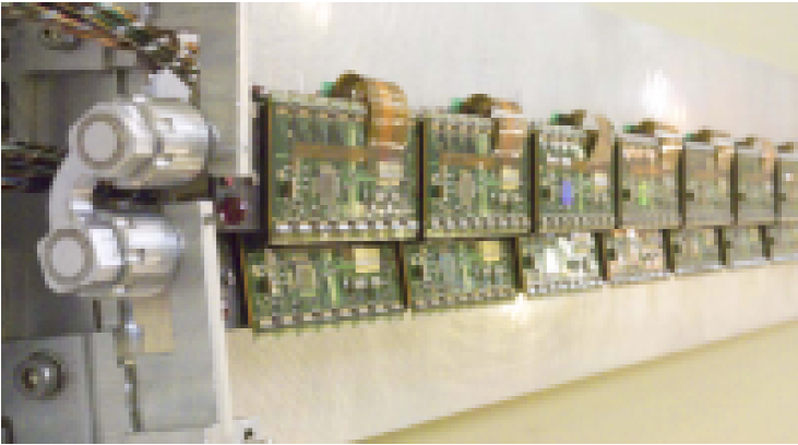
The modules are loaded onto carbon-fiber structures in three sites. For the endcap (Fig. 5), six modules are mounted on a sector assembly plate corresponding to 1/8 of a disk. Two subsequent disks are rotated to optimize coverage. For the barrel (Fig. 6), 13 modules are precisely glued on a stave. A quick connectivity test for all modules is performed to exclude damage during loading. The components are then sent to CERN for final integration.
| layer | barrel | endcaps |
|---|---|---|
| inner | 0.13% | 0.04% |
| center | 0.17% | 0.16% |
| outer | 0.27% | 0.22% |
A maximum ranking value of 60 edc was required for a module to be integrated on a stave for the innermost layer. Table 1 shows the fraction of dead channels per module, averaged over all modules which have been integrated into the detector.
5 Integration status
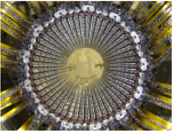
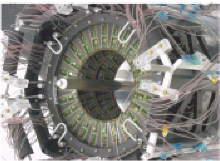
At the time of writing the three barrel layers and the two endcaps have been fully assembled. One endcap is being tested on a cosmic-ray setup, while the barrel layers are arranged in their final position around the beam pipe. Fig. 7 shows the completed outermost barrel layer. All modules are connected and tested to work properly with minor degradation with respect to the previous laboratory tests. In parallel, a system test has been setup to assess the read-out and DAQ readiness system .
During construction, a number of unforeseen issues and potential bottlenecks for the final detector completion arose and solutions were found.
To protect the delicate wirebonds of the front-end chips, of the pigtail connection and of the MCC, a protective coating (potting) is applied to prevent accidental mechanical breakage. During thermal stress tests a number of bonds connecting the MCC to the flex broke. While thorough studies demonstrated that a similar effect is not observed for the other potted bonds, it was decided to manually remove the potting on the MCCs and rebond them, which was achieved with 100% efficiency, even on dressed modules.
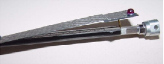
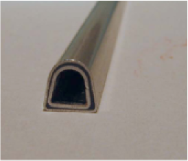
Two problems connected to the stave design were detected at a relatively late stage of production. Owing to the non-circular cross-section of the cooling pipe and the pressure of the coolant and the particular linear geometry of the stave, delamination of the carbon-carbon structure from the cooling pipe has been observed. This problem was resolved by adding a peek collar to the stave extremities (Fig. 8 left). Secondly, some cooling pipes were discovered to be leaky due to corrosion. The cause was found to be the brazing of the cooling fitting followed by a not accurate enough quality control (water vapor in the pipe). Cooling tubes and fittings were designed and laser welded in a new production. For existing, unloaded staves, the cooling pipe was replaced. For the approximately 40 already loaded staves, new pipes were inserted into the old ones (Fig. 8 right) providing a still satisfactory thermal contact.
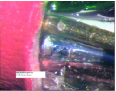
During loading of the first barrel staves, failures of some low-mass cables were observed at the pigtail connector junction due to excessive stress on the - thick wires. After closer inspection, cracks in the insulation of the power cables (Fig. 9) were discovered in an important fraction of the cables. The specific production technique was identified as the origin of the failure, and was corrected in time. A second batch of cables produced with the rectified process did not exhibit this problem.
6 Summary
A short description of the ATLAS pixel detector has been presented. The radiation environment and occupancy demanded the development of new technologies that started more than ten years ago. The project recently finished the module production and integration phase. Several issues were discovered and solved. Installation of the three-layer pixel detector is currently planned by April 2007 and is on schedule.
The three-layer pixel detector is currently expected to be installed as the last sub-detector into ATLAS on schedule by April 2007.
7 Acknowledgements
The development and construction of the ATLAS pixel detector involves more than 100 dedicated scientists and engineers from Berkeley, Bonn, Dortmund, Geneva, Genoa, Marseilles, Milan, New Mexico, Ohio, Oklahoma, Prague, Siegen, Udine and Wuppertal. This work is partially funded by BMBF under contract 05 HA4PD1/5.
References
- (1) Technical design report of the ATLAS pixel detector, CERN/LHCC 98-13, Geneva 1998.
- (2) M. S. Alam et al., Nucl. Instr. and Meth. A 456 (2001) 217.
- (3) A. Andreazza, Nucl. Instr. and Meth. A 565 (2006) 23.
- (4) I. Perić et al., Nucl. Instr. and Meth. A 565 (2006) 178.
- (5) R. Beccherle et al., Nucl. Instr. and Meth. A 492 (2002) 117.
- (6) J. Grosse-Knetter, Nucl. Instr. and Meth. A 568 (2006) 252.
- (7) C. Schiavi, these proceedings; J. Grosse-Knetter et al., Nucl. Instr. and Meth. A 565 (2006) 79.