Bandwidth control of forbidden transmission gaps in compound structures with subwavelength slits
Abstract
Phase resonances in transmission compound structures with subwavelength slits produce sharp dips in the transmission response. For all equal slits, the wavelengths of these sharp transmission minima can be varied by changing the width or the length of all the slits. In this paper we show that the width of the dip, i.e., the frequency range of minimum transmittance, can be controlled by making at least one slit different from the rest within a compound unit cell. In particular, we investigate the effect that a change in the dielectric filling, or in the length of a single slit produces in the transmission response. We also analyze the scan angle behavior of these structures by means of band diagrams, and compare them with previous results for all-equal slit structures.
pacs:
78.67.-n, 78.67.+m, 42.79.Dj, 42.25.Bs, 42.25.Fx, 42.70.QsI Introduction
The possibility of designing the transmission response of periodic structures with subwavelength slits has attracted the interest of the scientific community since these systems show promise for applications such as the characterization of attosecond pulses apb , integrated polarizers jvs , optical data storage and external storage media. Also, a great effort has been devoted to the modeling of scattering by thick metallic plates with 1D Porto ; Garcia-Vidal ; Xie2 and 2D Popov periodic perforations since the experimental demonstration of enhanced transmission by Ebbesen et al. Ebbesen ; Ghaemi . Most of the studies carried out in connection with this phenomenon consider simple structures, i.e., periodic structures in which a unit cell is defined by a single hole or slit.
Recent simulations reported in letter1_rd ; letter2_rd ; diana16 suggest that compound gratings (periodic structures comprising several slits in each unit-cell) can exhibit sharp transmission nulls when illuminated by -polarized plane waves of particular frequencies. These sharp dips correspond to the excitation of phase resonances in the structure, which arise from a particular phase and amplitude distribution of the magnetic field in adjacent cavities of a unit cell, and are characterized by a field enhancement within the slits. The behaviour of phase resonances in compound structures with subwavelength slits under oblique illumination has been studied recently diana16 , where the authors show that new phase modes, and therefore new transmission dips, that were not allowed for normal illumination due to symmetry reasons, appear for non-normal incidence.
Phase resonances were first reported in structures comprising a finite number of cavities on a perfect conductor Veremey3 ; dv1 , and later observed in compound reflection gratings under normal sad1 ; sad2 ; sad3 and oblique rsad1 illumination. Le Perchec et al. analyzed the excitation of these resonances in a two-slit system LePerchec . The additional parameters in the complex structure should allow for more degrees of freedom in the design of components such as nonlinear devices and frequency selective surfaces. Besides, for a selected region of the electromagnetic spectrum, the behavior of these complex structures can be compared to the effect produced by a defect in a photonic crystal (PC) Joannopoulos . Whereas a defect in a PC allows transmission within a forbidden band, a phase resonance in a compound transmission grating inhibits transmission in a highly transmitting region diana16 .
Recently, experimental demonstration of phase resonances in infinite compound gratings has been reported Hibbins-fase . In this paper, the authors confirm earlier predictions made by Skigin and Depine in letter1_rd and show that a structure comprising three slits within each period, illuminated at normal incidence, exhibits a dip in the transmission response within each Fabry-Perot resonance peak.
The theoretical approach used in this paper to model the 1D compound transmission grating is based on the Generalized Scattering Matrix (GSM) formulation. It basically consists in expanding the fields in each region in its own eigenmodes and then matching them imposing the boundary conditions. Oblique excitations of both thick and thin simple periodic frequency selective surfaces with arbitrary aperture cross-sections have been successfully analyzed with this approach GSM1 ; GSM2 ; GSM3 , which has been recently extended to deal with periodic structures comprising complex unit cells AP_Jacques ; Jacques_thesis . One advantage of the Extended Generalized Scattering Matrix (EGSM) formulation is that the individual GSM matrices describing any single discontinuity can be calculated separately and often a priori in a coordinate system best suited for an analytical solution. The assembly of GSMs describing a multitude of transverse discontinuities (i.e. multiple perforations per unit cell) forms a coordinate invariant EGSM that are easily cascaded via standard operators for problems having arbitrary longitudinal complexity. This abstraction alleviates tedious coordinate notation and facilitates fast parallel computation of electromagnetic scattering from highly complex unit cells.
The purpose of this paper is to show the design flexibility that compound gratings give for getting particular responses. We investigate the effect produced by a change in the dielectric constant and in the length of a single slit within each period. We also analyze the dependence of the response on the angle of incidence.
In Sec. II we summarize the extended generalized scattering matrix (EGSM) formulation used to solve the diffraction problem of a -polarized plane wave by a compound structure. In Sec. III we show numerical examples that illustrate the possibilities that these structures provide, by varying the dielectric filling as well as the length of the slits. We also show band diagrams that permit to visualize the angular dependence of the resonant frequencies and the bandwidth of the gaps, and compare them with those obtained for all-equal slits structures. Concluding remarks are given in Sec. IV.
II The Extended Generalized Scattering Matrix formulation
The EGSM is an extension of the Mode Matching-Generalized Scattering Matrix (MMGSM) method that allows computationally efficient solutions to a larger class of scattering problems. The method is capable of efficiently analyzing the reflection and transmission properties of TE- and TM- polarized plane waves incident at arbitrary angles onto thin or thick arbitrarily shaped frequency selective surfaces, gratings with generalized profiles, metal structures with multiple layers of dielectric fillings and/or coatings. The geometry of the scatterer can be periodic or aperiodic, transmitting and/or reflecting.
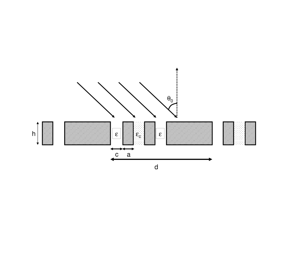
In the present case, we consider an infinitely periodic one-dimensional compound structure: each period comprises several perfectly conducting wires and three equal-width slits between wires are formed. Each slit can be filled with a different dielectric, as shown in Fig. 1. In what follows we summarize the fundamentals of the method. Further details are found in AP_Jacques ; Jacques_thesis .
The structure is divided longitudinally into slices or waveguide sections. These sections and the interfaces between them are represented by their equivalent EGSM and , respectively, where the subscript denotes the number of a transition () or guiding section (). To obtain the required transition and guided-section EGSMs, the fields in each slit are represented by modal expansions and appropriate boundary conditions are enforced at each transition: continuity of tangential electric fields in the open regions, null electric field on the perfect conductor, and continuity of tangential magnetic field. The equations resulting from these conditions are projected in convenient bases, which yields a matrix equation with the modal amplitudes towards and away from the transition as unknowns. Once all the guided sections and transition matrices are found, they are cascaded to find a relationship between the incident plane wave and the reflected and transmitted amplitudes AP_Jacques ; Jacques_thesis .
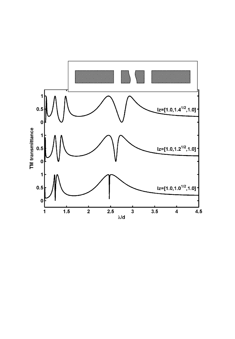
In the case of a uniformly filled waveguide with arbitrary longitudinal profile, where reflections from the gradual bends are negligible, it is sufficient to consider it as a straight section of the same waveguide having the length of the bent waveguide Lewin ; Katsenelenbaum . This is the case of the examples shown in Fig. 5.
III Results
The results shown illustrate the evolution of the phase resonances in a perfectly conducting compound thick-metal grating comprising three rectangular slits filled with different dielectrics. In the examples we consider symmetric structures in which the central slit can be different from the external ones in its dielectric filling (see Fig. 1) and eventually in its length (see inset of Fig. 5). A -polarized plane wave impinges on the structure in all the examples shown.
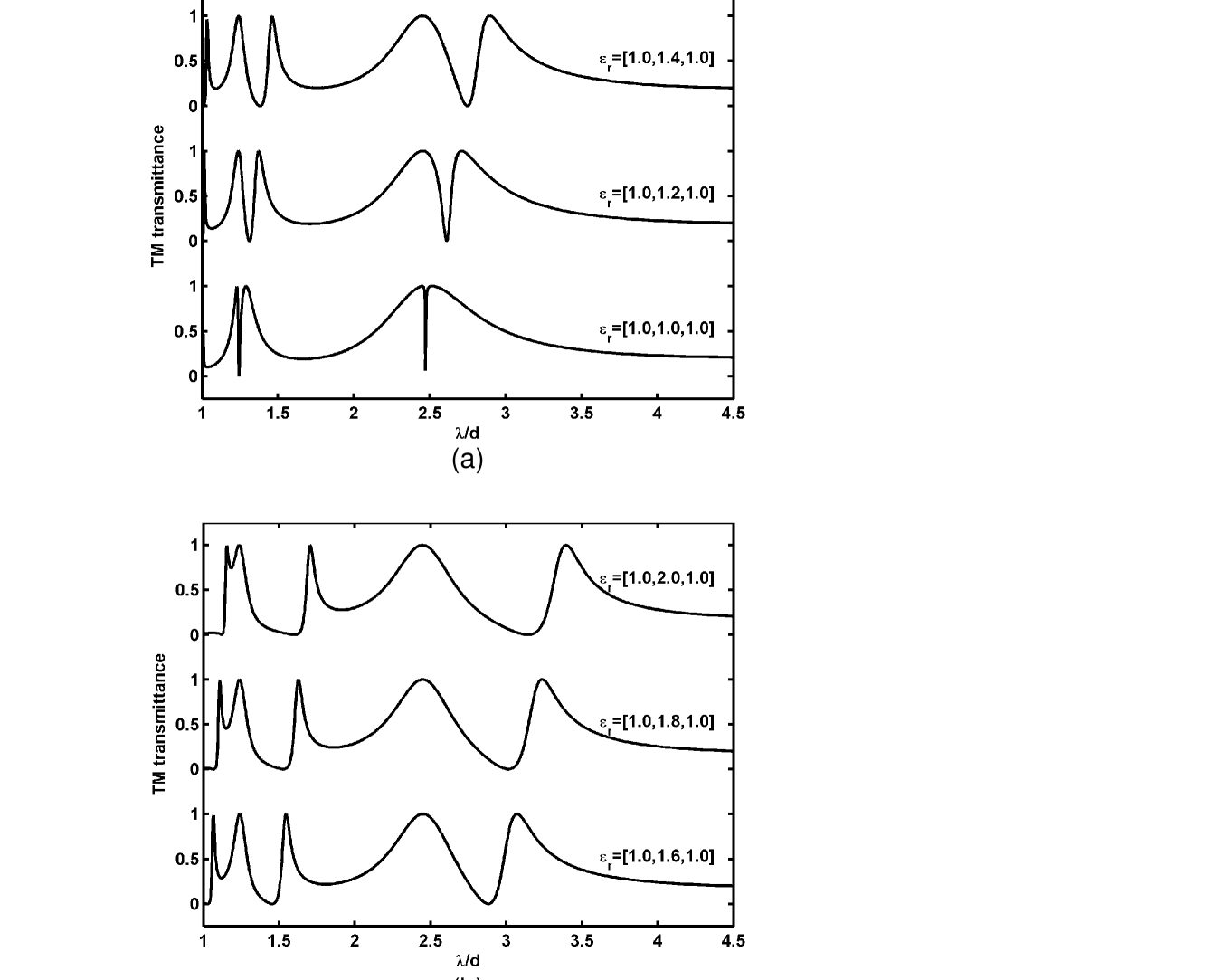
In Fig. 2 we show a sequence of curves when varying the dielectric constant of the central slit filling () while keeping all the rest of the parameters fixed: , , , . We plot the zero-order transmittance as a function of the incident wavelength for six cases: = 1, 1.2, 1.4, 1.6, 1.8, 2. The lower curve corresponds to identical slits, and the phase resonance appears as a sharp dip within the waveguide resonant peak of the slits. Phase resonances are produced in compound gratings due to the possibility of having different configurations of the field phase distribution within the different slits comprising each period of the structure letter1_rd . In particular, for three slits within the period, only one resonance is expected for normal incidence: the (+ - +) mode, i.e., the mode in which the phases of adjacent slits are reversed. The number of possible phase configurations is finite and depends on the number of slits. A mathematical criterion governing the resonances using the EGSM formalism is given in AP_Jacques ; Jacques_thesis .
In general, two requirements are needed for a phase resonance to occur: i) at least one non-zero phase difference is found between the field phases in adjacent slits —what is not allowed in simple periodic structures— and ii) a particular distribution of the field amplitude, naturally generated by the incidence conditions, is obtained dv1 . Phase resonances are also characterized by a strong intensification of the field inside the slits or inside the cavities, in the case of compound reflection gratings sad1 . In particular, when the phases in adjacent slits are opposite to each other, resonances can be excited dv1 . Regarding each slit as a waveguide, these two conditions are usually fulfilled within the waveguide mode resonant wavelength.
It can be observed that as the permittivity of the central slit is increased, the width of each phase resonance dip also increases. This suggests that the bandwidth of the narrow gaps generated by means of phase resonance excitations can be controlled. This characteristic makes this structure attractive from the point of view of several applications, such as filters and polarizers. It can also be regarded as a complementary structure to the photonic crystal. A typical band diagram of a photonic crystal presents band gaps, i.e., frequency ranges that are not allowed to propagate inside the crystal and therefore, if the structure is illuminated by a plane wave of a frequency within the gap, all the power is reflected Joannopoulos . However, if the perfect periodicity of the photonic crystal is broken by a defect in the structure, allowed states arise within the gap, enabling transmission within the originally forbidden gap. In the compound gratings considered in this paper, the structures are essentially transmitting, at least within the waveguide resonance peaks, as observed in Figure 2. Thus, when a simple grating is illuminated by a plane wave of a wavelength within the waveguide resonance peak, most of the power is transmitted through the structure. The addition of complexity to the period in the form of a group of slits can be regarded as a defect in the perfect periodicity, and in this case one or more forbidden channels are formed within the allowed bands diana16 .
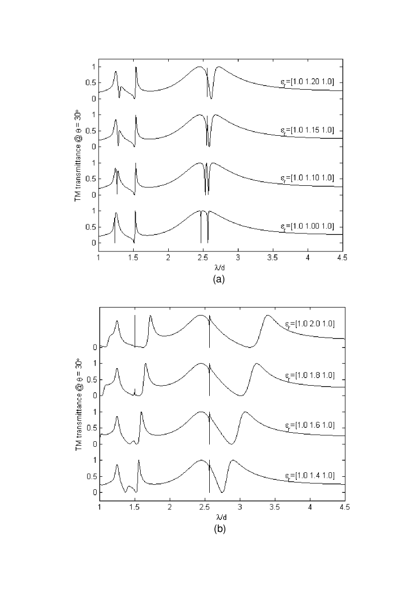
As it was already investigated in diana16 for all-alike slits structures, when compound gratings are obliquely illuminated, new possiblities of phase configurations within the slits open up, resulting in new phase resonances. For instance, for three equal slits we have the (+ - -) and the (+ + -) modes in addition to the one we had for normal incidence. To visualize the effect of changing the dielectric filling of the central slit in the response of the structure under oblique illumination, we show in Fig. 3 the transmittance for the same structure considered in Fig. 2, but for an oblique incidence: . It can be observed that now there are two dips within each waveguide resonance maximum, i.e., around and . For oblique incidence, the symmetry condition imposed by normal illumination is removed, and this allows new phase configurations inside the slits, which produce new dips in the transmission response. The resonance dip at slightly smaller than 2.5 for all equally filled slits (lower curve in Fig. 3(a)) shifts to larger wavelengths with decreasing quality factor () for small variations of the central dielectric constant (see the curve for ). From then on, it collapses into a very high- resonance for slightly larger than 2.5, and stays fixed throughout all further increases of . The dip for slightly larger than 2.5 in the lower curve () shifts to larger wavelengths with decreasing as increases. This behaviour suggests that both dips behave differently for variations in . The persistence of the high- resonance dip (leftmost dip within the peak) for all dielectric variations suggests that it is fixed by geometry and excitation, whereas the and the position of the rightmost dip are dielectric filling dependent. Besides, the transmittance peak to the left of the sharp null does not change much as is varied, whereas the peak to the right of the rightmost null is certainly tunable by changing the relative dielectric constant of the central slit filling.
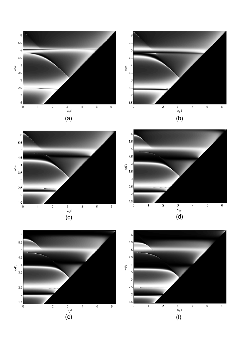
To get more insight about the influence of changing the central slit filling when the structure is obliquely illuminated, in Fig. 4 we show contour plots of the zero-order transmittance as a function of and , where is the incident wave vector component along the direction of periodicity and is the frequency of the incident wave. The lighter zones represent higher transmitted intensities. Fig. 4(a) corresponds to a compound structure with all-alike slits. It can be observed that there are mainly two transmission peaks, for 2.5 and 5. These maxima are scored by nulls, the number of which depends on the incidence angles: for normal illumination there is one dip within each peak, whereas for larger angles two dips are found within each peak. When the dielectric constant of the central slit filling is increased in steps of 0.2, we get the plots of Figs. 4(b) to 4(f) ( = 1.2, 1.4, 1.6, 1.8 and 2). It can be noticed that for normal incidence, the dip width increases with , as it was already observed in Fig. 2, and this trend is also maintained for the larger wavelenght dip at oblique incidence, as observed in Fig. 3 for . The results shown in Fig. 4 suggest that the phase resonance mechanism could be exploited not only to design structures with a prescribed number of resonances at specified wavelengths, but also to control their bandwidth by changing the dielectric filling.
The effect produced by changing the dielectric filling of the central slit in the transmitted response of the structure is similar to what occurs when the length of the central slit is changed. The propagation constant of each mode of a slit bounded by perfectly conducting walls and filled with a material with dielectric constant is:
| (1) |
where is the speed of light in vacuum and is an integer. Then, for a given length of the slit , the phase difference gained by the mode when going through the slit is . If the slit is now filled with another dielectric with , the new propagation constant is
| (2) |
and then the same phase difference would be obtained for another slit length such that
| (3) |
In particular, if the slit has a subwavelength width, as in the present case, the only propagating mode is the first mode, which corresponds to in (1) and (2). Then, condition (3) yields . Taking into account the above relationship between the length and the dielectric constant of the slit filling, it is to be expected that the response of a structure with a higher central permittivity should be similar to that of the structure comprising equally filled slits, but with a longer central slit. The EGSM method used to solve the diffraction problem allows for the treatment of bent waveguides with arbitrary longitudinal profile. Then, we increased the length of the central slit () by bending it slightly, as shown in the inset of Fig. 5. The results in Fig. 5 show the evolution of the transmitted intensity as the central slit length is increased, when keeping , for the same parameters considered in Fig. 2. It can be observed that the three curves (, and ) for are very similar to those of Fig. 2(a), for , 1.2 and 1.4 and . This result also shows that the resonance bandwidth can be controlled not only by changing the dielectric filling, but also by varying the length of the slits.
IV Conclusions
We have investigated the response of compound transmission wire gratings with subwavelength slits under oblique incidence. To solve the diffraction problem we used the EGSM method, which is very versatile. The ease of its formulation significantly reduces the time and effort required for more advanced structures. We focused in a structure comprising three slits in each period and analyzed the influence that a change in the dielectric filling and in the length of the central slit has over the resonant dip. We have shown numerical results that evidence the possibility of controlling the bandwidth of phase resonance dips by properly choosing the geometrical and constitutive parameters. The angular behavior of these structures was also analyzed by means of band diagrams, and the results obtained were compared with previous ones corresponding to all-equal slit structures. The capability of exciting and controlling the bandwidth of phase resonances in compound gratings opens up new possibilities for practical applications, such as polarization sensitive aperture shapes for field enhancement devices.
Acknowledgements
D. Skigin gratefully acknowledges Prof. Ricardo Depine for discussions and support from Consejo Nacional de Investigaciones Científicas y Técnicas (CONICET), Universidad de Buenos Aires (UBA, X150 and X2) and Agencia Nacional de Promoción Científica y Tecnológica (ANPCYT-BID 1728/OC-AR-PICT 14099). Z. Popovic and H. Loui acknowledge support from a NSF International Supplement to a ITR Collaborative Research Grant No. CCR-0112591 and by the Department of Education Graduate Assistance in Areas of National Need (GAANN) Fellowship in Hybrid Signal Electronics (HYSE), award #P200A040154. This research was also supported in part by an appointment to the Sandia National Laboratories Truman Fellowship in National Security Science and Engineering, sponsored by Sandia Corporation as Operator of Sandia National Laboratories under its U.S. Department of Energy Contract No. DEAC0494AL85000.
References
- (1) E. Goulielmakis, G. Nersisyan, N. Papadogiannis, D. Charalambidis, G. Tsakiris, and K. Witte, “A dispersionless Michelson interferometer for the characterization of attosecond pulses”, Appl. Phys. B 74, 197 206 (2002).
- (2) Jian Jim Wang, Feng Liu, Xuegong Deng, Xiaoming Liu, Lei Chen, Paul Sciortino, and Ron Varghese, “Monolithically integrated circular polarizers with two-layer nano-gratings fabricated by imprint lithography”, Journal of Vacuum Science & Technology B: Microelectronics and Nanometer Structures 23, 3164-3167 (2005).
- (3) J. A. Porto, F. J. García-Vidal and J. B. Pendry, “Transmission resonances on metallic gratings with very narrow slits”, Phys. Rev. Lett. 83, 2845-2848 (1999).
- (4) F. J. García-Vidal and L. Martín-Moreno, “Transmission and focusing of light in one-dimensional periodically nanostructures metals”, Phys. Rev. B 66, 155412 (2002).
- (5) Y. Xie, A. R. Zakharian, J. V. Moloney and M. Mansuripur, “Transmission of light through a periodic array of slits in a thick metallic film”, Opt. Express 13, 4485-4491 (2005).
- (6) E. Popov, M. Neviere, S. Enoch and R. Reinisch, “Theory of light transmission through subwavelength periodic hole arrays”, Phys. Rev. B 62, 16100-16108 (2000).
- (7) T. W. Ebbesen, H. J. Lezec, H. F. Ghaemi, T. Thio and P. A. Wolff, “Extraordinary optical transmission through sub-wavelength hole arrays”, Nature 391, 667-669 (1998).
- (8) H. F. Ghaemi, T. Thio, D. E. Grupp, T. W. Ebbesen and H. J. Lezec, “Surface plasmons enhance optical transmission through subwavelength holes”, Phys. Rev. B 58, 6779-6782 (1998).
- (9) D. C. Skigin and R. A. Depine, “Transmission resonances on metallic compound gratings with subwavelength slits”, Phys. Rev. Lett. 95, 217402 (2005), (paper selected for publication in the Virtual Journal of Nanoscale Science and Technology http://www.vjnano.org/nano/ 12, (22) (2005)).
- (10) D. C. Skigin and R. A. Depine, “Resonances on metallic compound transmission gratings with subwavelength wires and slits”, Opt. Commun. 262, 270-275 (2006).
- (11) D. C. Skigin and R. A. Depine, “Narrow gaps for transmission through metallic structured gratings with subwavelength slits”, Phys. Rev. E 74, 046606 (2006).
- (12) V. V. Veremey and R. Mittra, “Scattering from structures formed by resonant elements”, IEEE Trans. on Antennas Propag. 46, 4, 494-501 (1998).
- (13) D. C. Skigin, V. V. Veremey and R. Mittra, “Superdirective radiation from finite gratings of rectangular grooves”, IEEE Trans. on Antennas Propag. 47, (2), 376-383 (1999).
- (14) A. N. Fantino, S. I. Grosz and D. C. Skigin, “Resonant effects in periodic gratings comprising a finite number of grooves in each period”, Phys. Rev. E 64 (1), 016605 (2001).
- (15) S. I. Grosz, D. C. Skigin and A. N. Fantino, “Resonant effects in compound diffraction gratings: influence of the geometrical parameters of the surface”, Phys. Rev. E 65 (5), 056619 (2002).
- (16) D. C. Skigin, A. N. Fantino and S. I. Grosz, “Phase resonances in compound metallic gratings”, J. Opt. A: Pure Appl. Opt. 5, S129-S135 (2003).
- (17) R. A. Depine, A. N. Fantino, S. I. Grosz and D. C. Skigin, “Phase resonances in obliquely illuminated compound gratings”, Optik Int. J. Light Electr. Opt. (in press, January 2006).
- (18) J. Le Perchec, P. Quemerais, A. Barbara, and T. López-Ríos, “Controlling strong electromagnetic fields at subwavelength scales”, Phys. Rev. Lett. 97, 036405 (2006).
- (19) J. D. Joannopoulos, R. D. Meade and J. N. Winn, Photonic Crystals, Princeton University Press, United Kingdom, 1995.
- (20) A. P. Hibbins, I. R. Hooper, M. J. Lockyear and J. R. Sambles, “Microwave transmission of a compound metal grating”, Phys. Rev. Lett. 96, 257402 (2006).
- (21) B. Widenberg, “A general mode matching technique applied to bandpass radomes,” Lund Institute of Technology Department of Electroscience, Lund, Sweden, Electromagnetic Theory Tech. Rep. TEAT-7098, Aug. 2001.
- (22) A. Monorchio, P. Grassi, and G. Manara, “A hybrid mode-matching finite-elements approach to the analysis of thick dichroic screens with arbitrarily shaped apertures, IEEE Antennas and Wireless Propag. Letters 1, 120 123 (2002).
- (23) B. Widenberg, S. Poulsen, and A. Karlsson, “Thick screens perforated with a periodic array of apertures with arbitrary cross-section,” Lund Institute of Technology Department of Electroscience, Lund, Sweden, Electromagnetic Theory Tech. Rep. TEAT-7082, June 1999.
- (24) Hung Loui, Edward F. Kuester, Diana Skigin and Zoya Popovic, “A General Method for the Analysis of Electromagnetic Scattering from Metal Gratings and Frequency Selective Surfaces”, IEEE Transactions on Antennas Propag. (submitted, 2006).
- (25) Hung Loui, “Modal analysis and design of compound gratings and frequency selective surfaces”, Ph.D. dissertation, University of Colorado, Boulder, June 2006.
- (26) L. Lewin, D. C. Chang, and E. F. Kuester, Electromagnetic Waves and Curved Structures, ser. IEE Electromagnetic Waves. Stevenage, England: Peter Peregrinus LTD., 1977, vol. 2.
- (27) B. Z. Katsenelenbaum, L. M. del Río, M. Pereyaslavets, M. S. Ayza, and M. Thumm, Theory of Nonuniform Waveguides - the cross-section method, ser. IEE Electromagnetic Waves. London, UK: IEE, 1998, vol. 44.